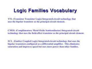
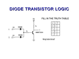
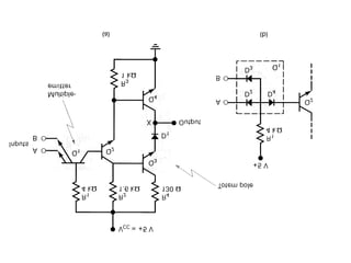
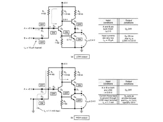
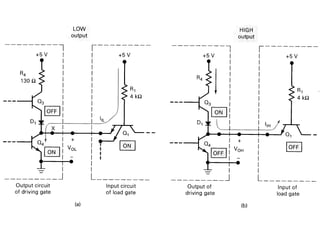
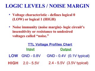
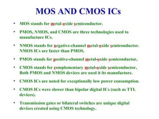
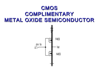
Digital ElectronicsDigital Electronics
Logic Families
TTL and CMOS
Logic Families CompetenciesLogic Families Competencies
61. Without references the student will state what the
acronym TTL stands for with 100% accuracy.
62. Without references the student will state the voltage
levels acceptable to a TTL input for a logic “0” and a logic
“1” with 100% accuracy.
63. Without references the student will state what the
acronym CMOS stands for with 100% accuracy.
64. Without references the student will state the voltage
levels acceptable to a CMOS input for a logic “0” and a logic
“1” with 100% accuracy.
65. Without references, the student will list three
differences between the TTL and CMOS logic families with
100% accuracy.
66. Without references the student will state what the
acronym ECL stands for with 100% accuracy.
Logic Families VocabularyLogic Families Vocabulary
TTL (Transistor Transistor Logic) Integrated-circuit technology that
uses the bipolar transistor as the principal circuit element.
CMOS (Complimentary Metal Oxide Semiconductor) Integrated-circuit
technology that uses the field-effect transistor as the principal circuit element.
ECL (Emitter Coupled Logic) Integrated-circuit technology that uses the
bipolar transistors configured as a differential amplifier. This eliminates
saturation and improves speed but uses more power than other families.
DIODE TRANSISTOR LOGICDIODE TRANSISTOR LOGIC
Y
What logicfunctionisthiscircuit?
11
01
10
00
YAA
FILL IN THE TRUTH TABLE
DIODE TRANSISTOR LOGIC
B
A
0V
0V
+V
5V
DIODE
DIODE
MMBT3904
1k
1k
LOGIC LEVELS / NOISE MARGIN
• Voltage characteristic - defines logical 0
(LOW) or logical 1 (HIGH)
• Noise immunity (noise margin)- logic circuit’s
insensitivity or resistance to undesired
voltages called “noise.”
Input Output
2.0 - 5.5V
LOW GND - 0.8V
HIGH 2.4 - 5.5V (3.5V typical)
GND - 0.4V (0.1V typical)
TTL Voltage Profiles Chart
0%
10%
60%
50%
80%
70%
40%
30%
20%
100%
90%
HIGH
LOW
HIGH
LOW
TTL CMOS
LOW
0 to +3V for CMOS
0 to +0.8V in TTL
Input Voltage Profiles
INPUT VOLTAGE PROFILES-
TTL AND 4000 SERIES CMOS
Undefined
+3 to +7V for CMOS
+0.8V to +2.0V for TTL
Undefined
logic probe reading may
vary depending on
manufacturer
HIGH
+7V to +10V - CMOS
+2V to +5V - TTL
CAUTION
Output V profile differs
Other families V profile differs
+5V +10V
GND
H
Low
+5V
+2V
+0.8V
GND
INPUT
H
Low
+5V
+2.4V
+0.4V
GND
OUTPUT
? ?
Input = +4V
Output = ? ?HIGH
Input = +0.3V
Output = ? LOW
Input = +1.2V
Output = ? ?Undefined
Input = +2.2V
Output = ? ?HIGH
TTL Voltage Profiles
(Left mouse click for questions and answers)
TEST
OTHER DIGITAL IC SPECIFICATIONS
• Drive Capabilities- sometimes referred to as fan-in or
fan-out.
• Fan out- number of inputs of a logic family that can be
driven by a single output. The drive capability of
outputs.
• Fan in- the load an input places on an output.
• Propagation delay- has to do with the “speed” of the logic
element. Lower propagation delays mean higher speed
which is a desirable characteristic.
• Power Dissipation- generally, as propagation delays
decrease, power consumption and heat generation
increase. CMOS is noted for low power consumption.
MOS AND CMOS ICs
• MOS stands for metal-oxide semiconductor.
• PMOS, NMOS, and CMOS are three technologies used to
manufacture ICs.
• NMOS stands for negative-channel metal-oxide semiconductor.
NMOS ICs are faster than PMOS.
• PMOS stands for positive-channel metal-oxide semiconductor.
• CMOS stands for complementary metal-oxide semiconductor.
Both PMOS and NMOS devices are used it its manufacture.
• CMOS ICs are noted for exceptionally low power consumption.
• CMOS ICs were slower than bipolar digital ICs (such as TTL
devices).
• Transmission gates or bilateral switches are unique digital
devices created using CMOS technology.
1. The drive capability of logic device outputs is
sometimes called ___ (fan in, fan out). It is the
number of inputs of a logic family that can be
driven by a single output.
(Left click mouse for questions and answers)
Fan Out
2. CMOS devices are noted for their extremely ___
(high, low) power consumption.
Low
3. A logic device with a low propagation delay
would be considered to be a ___ (high, low) speed
device.
High
4. Several desirable characteristics of logic
devices are good drive capabilities, low power
consumption, and ___ (high, low) propagation
delays.
Low
TEST
MOSFETMOSFET
METAL OXIDE SEMICONDUCTORMETAL OXIDE SEMICONDUCTOR
FIELD EFFECT TRANSISTORSFIELD EFFECT TRANSISTORS
P-CHANNEL ENHANCEMENTP-CHANNEL ENHANCEMENT N-CHANNEL ENHANCEMENTN-CHANNEL ENHANCEMENT
TO TURN ON GATE MUST BE
LOWER THAN SOURCE
TO TURN ON GATE MUST BE
HIGHER THAN SOURCE
TO TURNON
GATELOWER
THANSOURCE
D
G
S
P-MOS Vout
Vin
C-MOS
P-MOS
N-MOS
TO TURNON
GATEHIGHER
THANSOURCE
G
S
D
N-MOS0V
+V
5V
10k
0V
5V
+V
5V
+V
5V
10k
TO TURNON
GATELOWER
THANSOURCE
D
G
S
P-MOS Vin
TO TURNON
GATEHIGHER
THANSOURCE
G
S
D
N-MOS0V
+V
5V
10k
0V
5V
+V
5V
10k
MOSFETMOSFET
METAL OXIDE SEMICONDUCTORMETAL OXIDE SEMICONDUCTOR
FIELD EFFECT TRANSISTORSFIELD EFFECT TRANSISTORS
CMOSCMOS
COMPLIMENTARYCOMPLIMENTARY
METAL OXIDE SEMICONDUCTORMETAL OXIDE SEMICONDUCTOR
CMOSCMOS
COMPLIMENTARYCOMPLIMENTARY
METAL OXIDE SEMICONDUCTORMETAL OXIDE SEMICONDUCTOR
Vout
Vin
C-MOS
P-MOS
N-MOS
0V
+V
5V
ECLECL
EMITTER COUPLED LOGICEMITTER COUPLED LOGIC

logic_families

  • 1.
  • 2.
    Logic Families CompetenciesLogicFamilies Competencies 61. Without references the student will state what the acronym TTL stands for with 100% accuracy. 62. Without references the student will state the voltage levels acceptable to a TTL input for a logic “0” and a logic “1” with 100% accuracy. 63. Without references the student will state what the acronym CMOS stands for with 100% accuracy. 64. Without references the student will state the voltage levels acceptable to a CMOS input for a logic “0” and a logic “1” with 100% accuracy. 65. Without references, the student will list three differences between the TTL and CMOS logic families with 100% accuracy. 66. Without references the student will state what the acronym ECL stands for with 100% accuracy.
  • 3.
    Logic Families VocabularyLogicFamilies Vocabulary TTL (Transistor Transistor Logic) Integrated-circuit technology that uses the bipolar transistor as the principal circuit element. CMOS (Complimentary Metal Oxide Semiconductor) Integrated-circuit technology that uses the field-effect transistor as the principal circuit element. ECL (Emitter Coupled Logic) Integrated-circuit technology that uses the bipolar transistors configured as a differential amplifier. This eliminates saturation and improves speed but uses more power than other families.
  • 4.
    DIODE TRANSISTOR LOGICDIODETRANSISTOR LOGIC Y What logicfunctionisthiscircuit? 11 01 10 00 YAA FILL IN THE TRUTH TABLE DIODE TRANSISTOR LOGIC B A 0V 0V +V 5V DIODE DIODE MMBT3904 1k 1k
  • 9.
    LOGIC LEVELS /NOISE MARGIN • Voltage characteristic - defines logical 0 (LOW) or logical 1 (HIGH) • Noise immunity (noise margin)- logic circuit’s insensitivity or resistance to undesired voltages called “noise.” Input Output 2.0 - 5.5V LOW GND - 0.8V HIGH 2.4 - 5.5V (3.5V typical) GND - 0.4V (0.1V typical) TTL Voltage Profiles Chart
  • 10.
    0% 10% 60% 50% 80% 70% 40% 30% 20% 100% 90% HIGH LOW HIGH LOW TTL CMOS LOW 0 to+3V for CMOS 0 to +0.8V in TTL Input Voltage Profiles INPUT VOLTAGE PROFILES- TTL AND 4000 SERIES CMOS Undefined +3 to +7V for CMOS +0.8V to +2.0V for TTL Undefined logic probe reading may vary depending on manufacturer HIGH +7V to +10V - CMOS +2V to +5V - TTL CAUTION Output V profile differs Other families V profile differs +5V +10V GND
  • 11.
    H Low +5V +2V +0.8V GND INPUT H Low +5V +2.4V +0.4V GND OUTPUT ? ? Input =+4V Output = ? ?HIGH Input = +0.3V Output = ? LOW Input = +1.2V Output = ? ?Undefined Input = +2.2V Output = ? ?HIGH TTL Voltage Profiles (Left mouse click for questions and answers) TEST
  • 12.
    OTHER DIGITAL ICSPECIFICATIONS • Drive Capabilities- sometimes referred to as fan-in or fan-out. • Fan out- number of inputs of a logic family that can be driven by a single output. The drive capability of outputs. • Fan in- the load an input places on an output. • Propagation delay- has to do with the “speed” of the logic element. Lower propagation delays mean higher speed which is a desirable characteristic. • Power Dissipation- generally, as propagation delays decrease, power consumption and heat generation increase. CMOS is noted for low power consumption.
  • 13.
    MOS AND CMOSICs • MOS stands for metal-oxide semiconductor. • PMOS, NMOS, and CMOS are three technologies used to manufacture ICs. • NMOS stands for negative-channel metal-oxide semiconductor. NMOS ICs are faster than PMOS. • PMOS stands for positive-channel metal-oxide semiconductor. • CMOS stands for complementary metal-oxide semiconductor. Both PMOS and NMOS devices are used it its manufacture. • CMOS ICs are noted for exceptionally low power consumption. • CMOS ICs were slower than bipolar digital ICs (such as TTL devices). • Transmission gates or bilateral switches are unique digital devices created using CMOS technology.
  • 14.
    1. The drivecapability of logic device outputs is sometimes called ___ (fan in, fan out). It is the number of inputs of a logic family that can be driven by a single output. (Left click mouse for questions and answers) Fan Out 2. CMOS devices are noted for their extremely ___ (high, low) power consumption. Low 3. A logic device with a low propagation delay would be considered to be a ___ (high, low) speed device. High 4. Several desirable characteristics of logic devices are good drive capabilities, low power consumption, and ___ (high, low) propagation delays. Low TEST
  • 15.
    MOSFETMOSFET METAL OXIDE SEMICONDUCTORMETALOXIDE SEMICONDUCTOR FIELD EFFECT TRANSISTORSFIELD EFFECT TRANSISTORS P-CHANNEL ENHANCEMENTP-CHANNEL ENHANCEMENT N-CHANNEL ENHANCEMENTN-CHANNEL ENHANCEMENT TO TURN ON GATE MUST BE LOWER THAN SOURCE TO TURN ON GATE MUST BE HIGHER THAN SOURCE
  • 16.
    TO TURNON GATELOWER THANSOURCE D G S P-MOS Vout Vin C-MOS P-MOS N-MOS TOTURNON GATEHIGHER THANSOURCE G S D N-MOS0V +V 5V 10k 0V 5V +V 5V +V 5V 10k TO TURNON GATELOWER THANSOURCE D G S P-MOS Vin TO TURNON GATEHIGHER THANSOURCE G S D N-MOS0V +V 5V 10k 0V 5V +V 5V 10k MOSFETMOSFET METAL OXIDE SEMICONDUCTORMETAL OXIDE SEMICONDUCTOR FIELD EFFECT TRANSISTORSFIELD EFFECT TRANSISTORS
  • 17.
  • 18.
    CMOSCMOS COMPLIMENTARYCOMPLIMENTARY METAL OXIDE SEMICONDUCTORMETALOXIDE SEMICONDUCTOR Vout Vin C-MOS P-MOS N-MOS 0V +V 5V
  • 19.