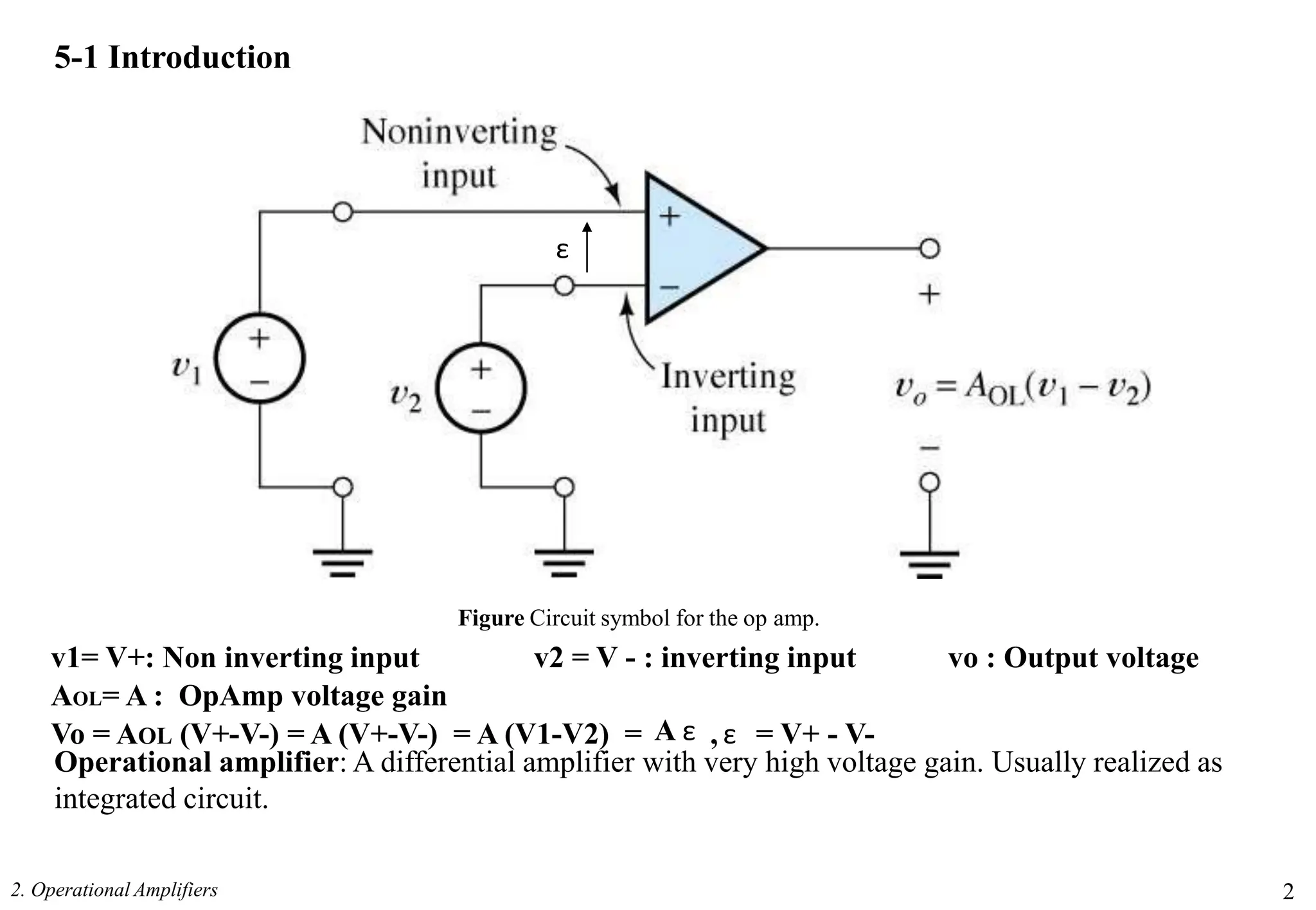
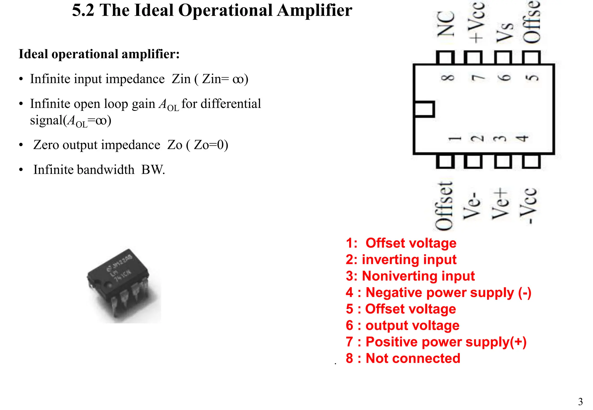
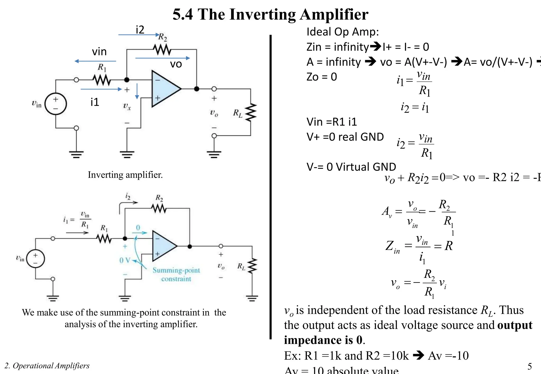
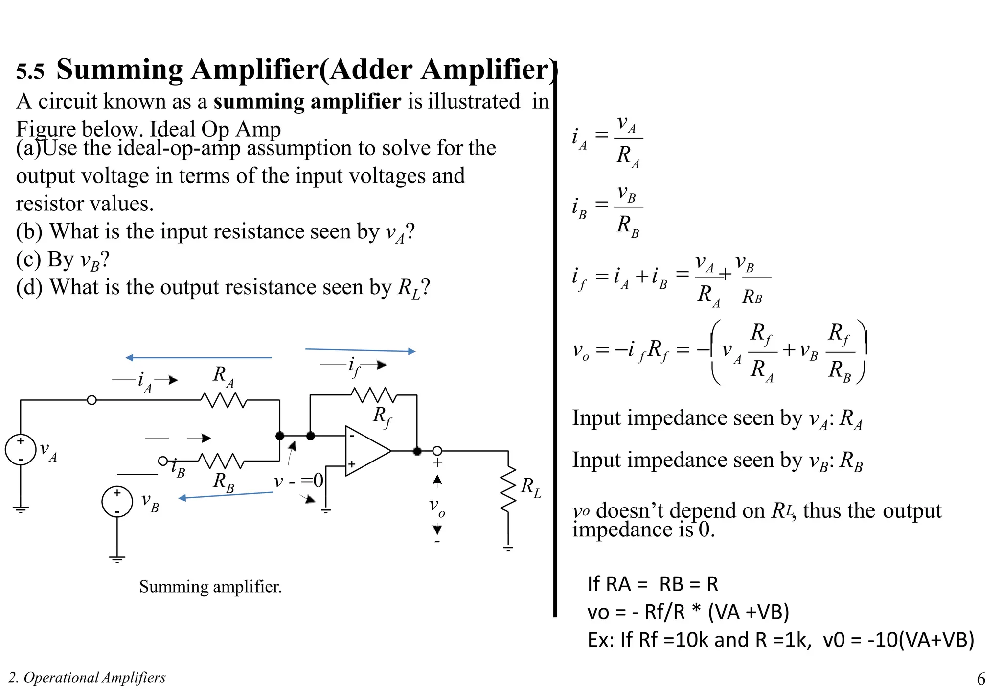
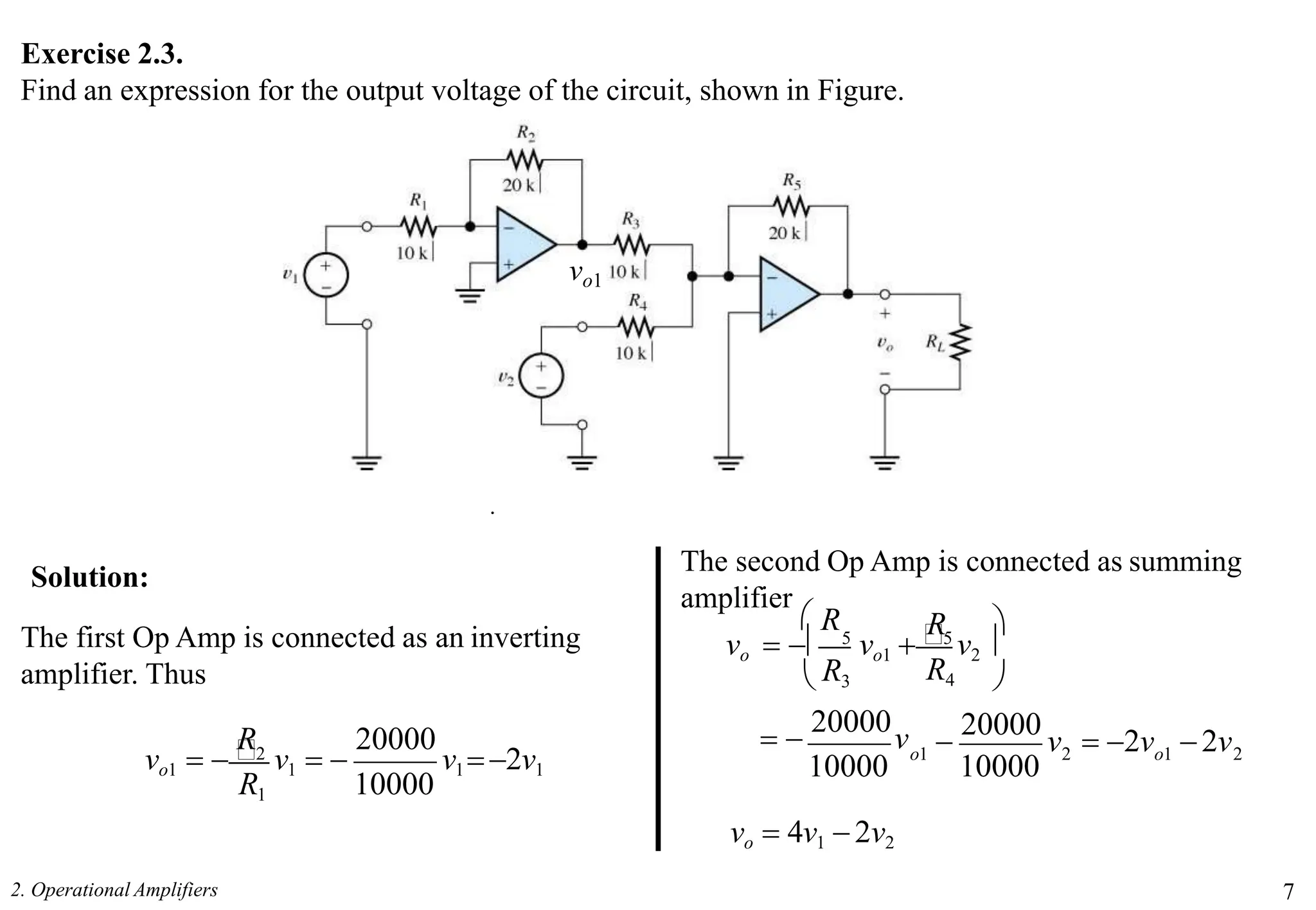
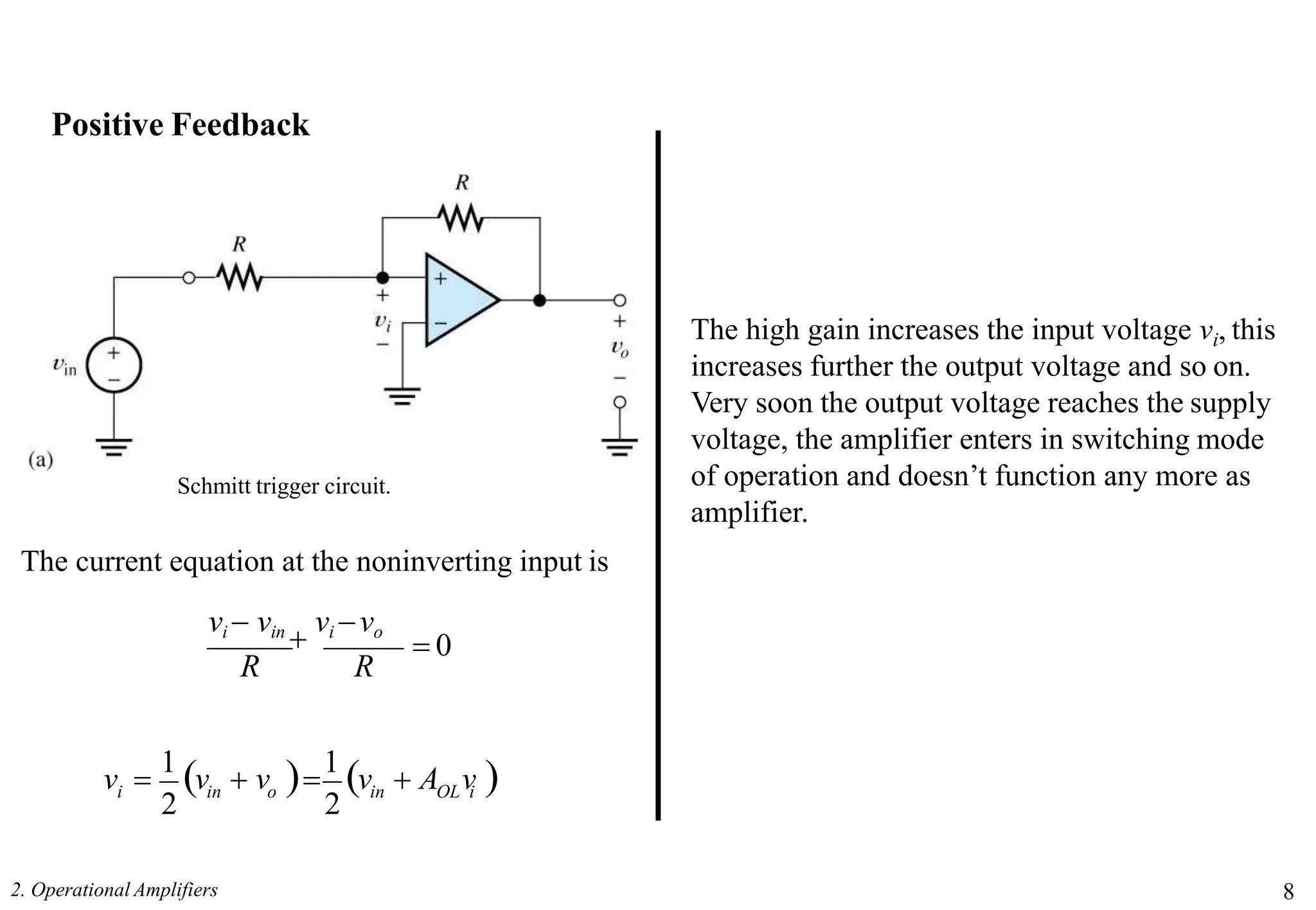
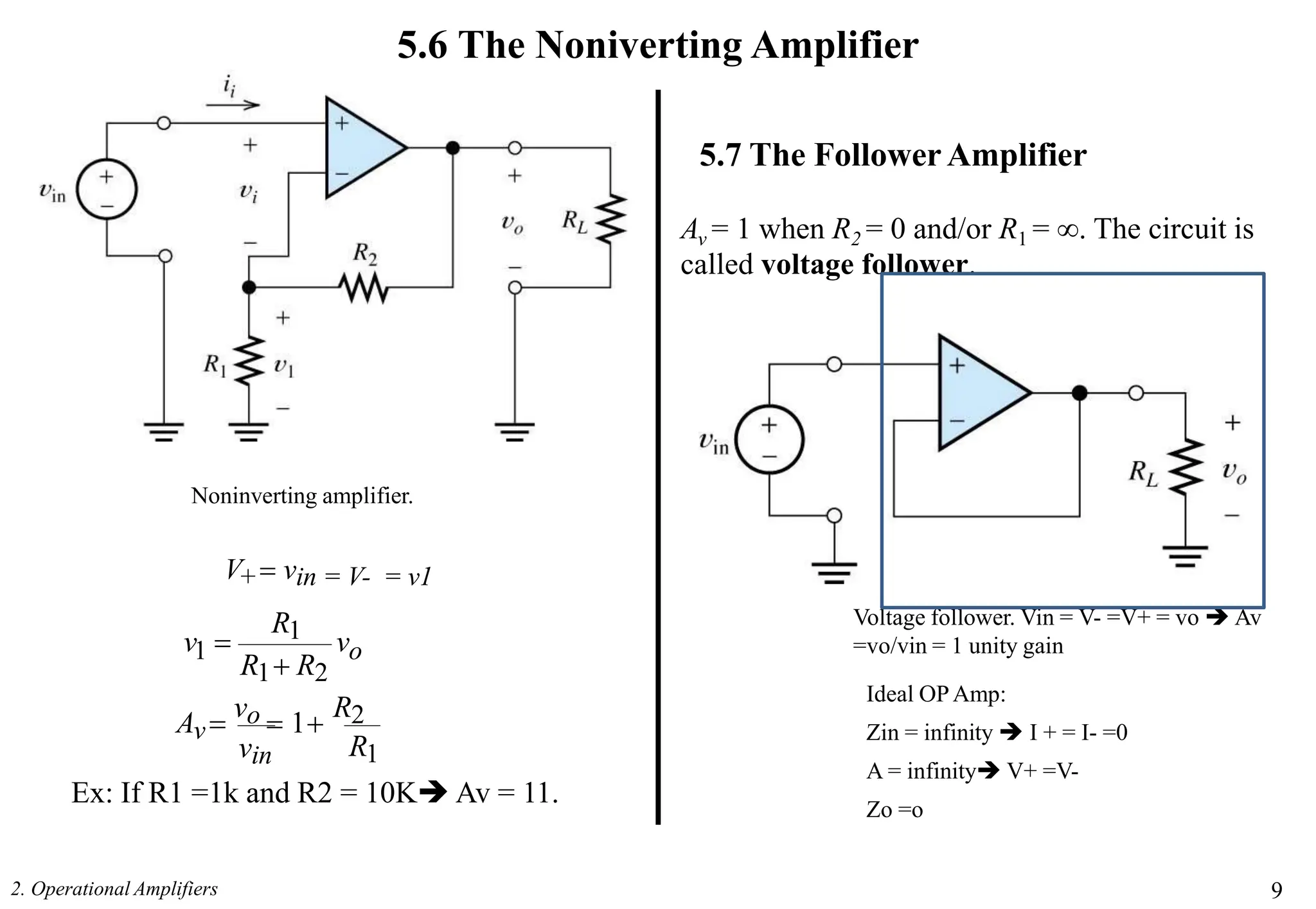
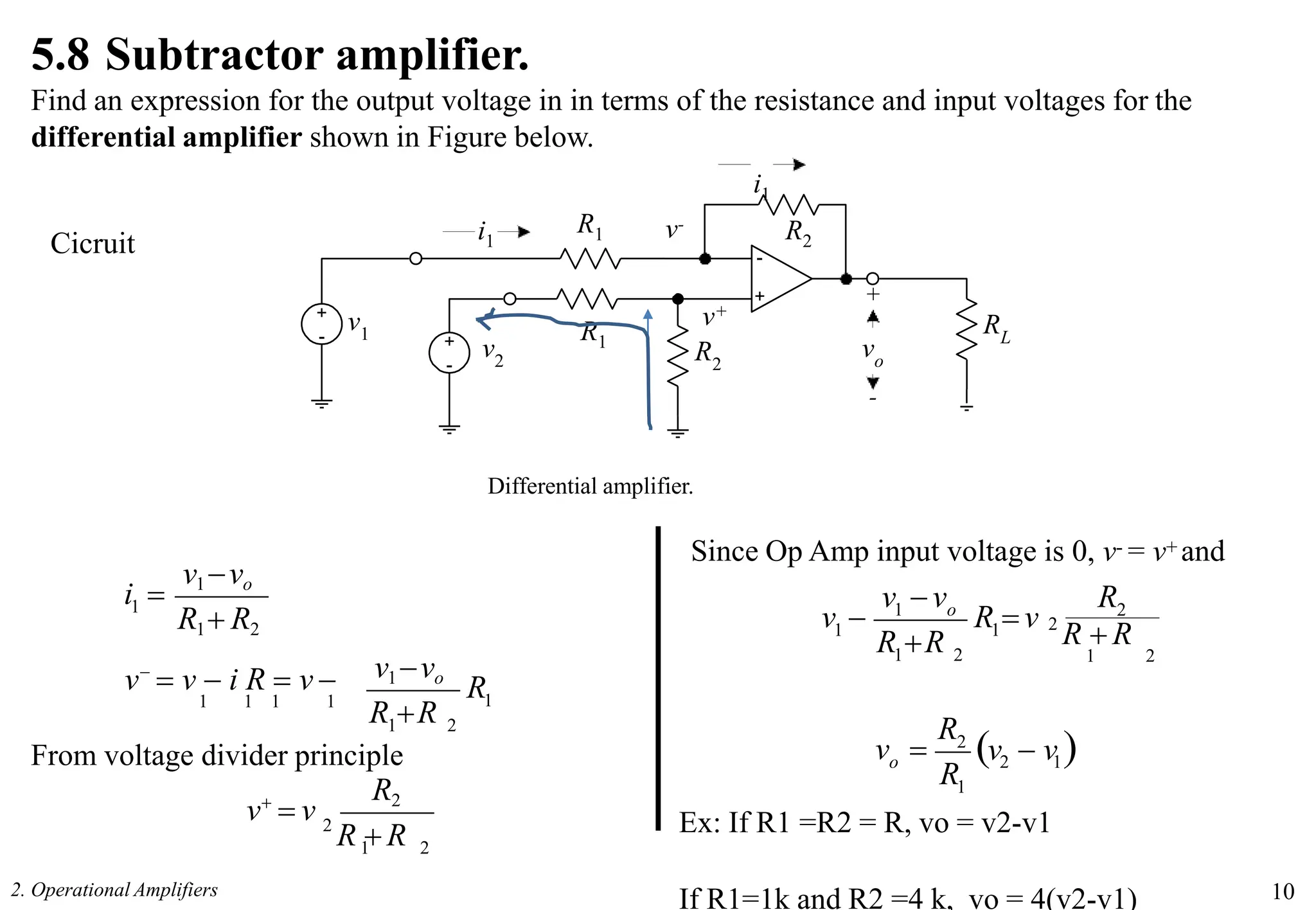
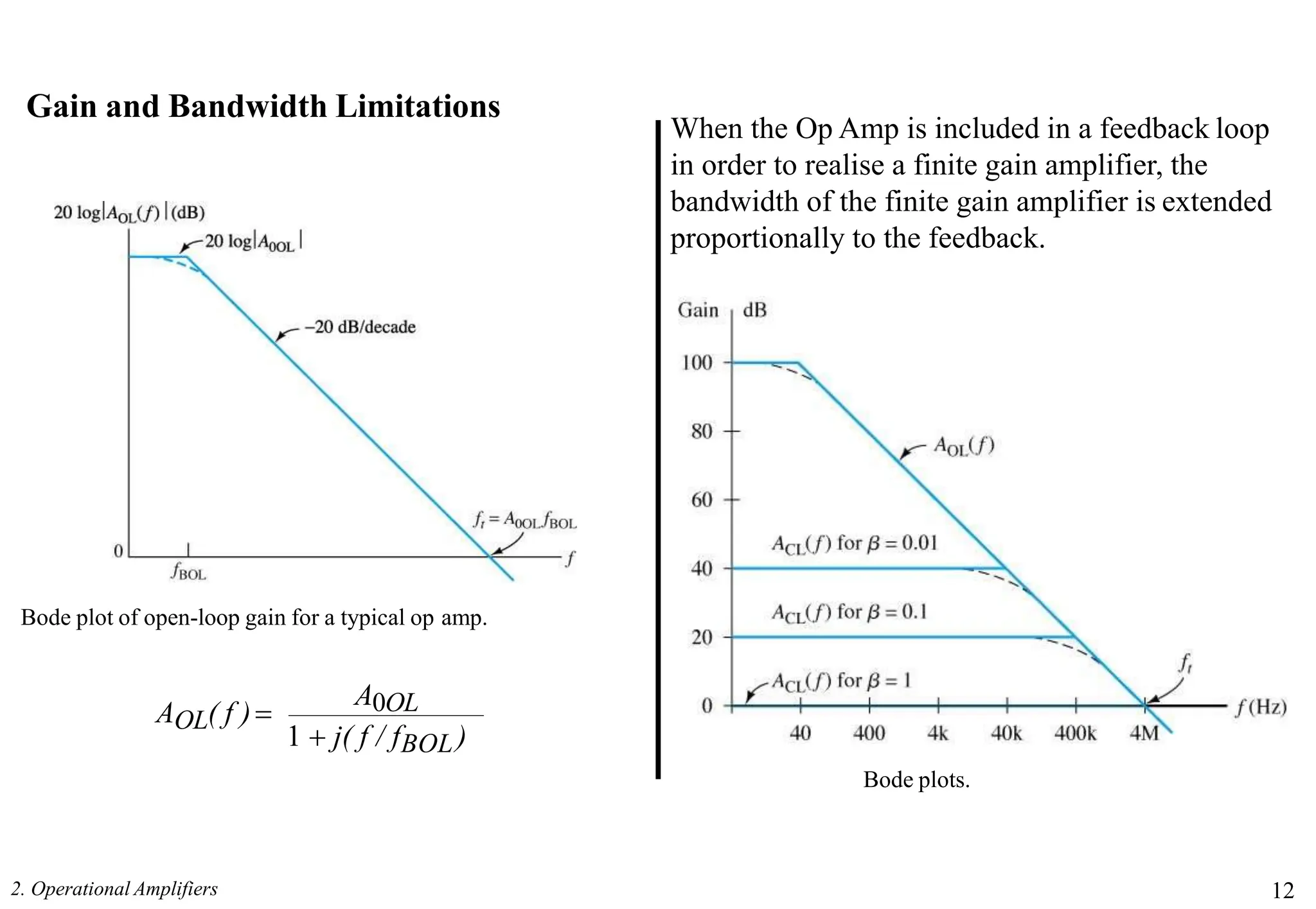
2. Figure Circuit symbol for the op amp.
2. Operational Amplifiers 2
Operational amplifier: A differential amplifier with very high voltage gain. Usually realized as
integrated circuit.
v1= V+: Non inverting input v2 = V - : inverting input vo : Output voltage
AOL= A : OpAmp voltage gain
Vo = AOL (V+-V-) = A (V+-V-) = A (V1-V2) = , = V+ - V-
5-1 Introduction
ε
A ε ε
3. 5.2 The Ideal Operational Amplifier
Ideal operational amplifier:
• Infinite input impedance Zin ( Zin= ꝏ)
• Infinite open loop gain AOL for differential
signal(AOL=ꝏ)
• Zero output impedance Zo ( Zo=0)
• Infinite bandwidth BW.
3
.
1: Offset voltage
2: inverting input
3: Noniverting input
4 : Negative power supply (-)
5 : Offset voltage
6 : output voltage
7 : Positive power supply(+)
8 : Not connected
4. 5.3 The Summing-Point Constraint
2. Operational Amplifiers 4
Operational amplifiers are almost always used with negative feedback, in which part of the op-
amp output signal is returned to the input in opposition to the source signal.
Ideal op-amp circuits are analyzed by the following steps:
1.Verify that the negative feedback is present. Usually this takes the form of a resistor network
connected to the output terminal and to the inverting input terminal.
2.Assume that the differential input voltage and the input current of the op amp are forced
to zero. (This is summing - point constraint.)
3.Apply standard circuit analysis principles, such as Kirchhoff’s laws and Ohm’s law, to solve
for the quantities of interest.
ε
5. 5.4 The Inverting Amplifier
i1
vin
R1
i2 i1
i2
vin
R1
vo R2i2 0=> vo =- R2 i2 = -R
Inverting amplifier.
1
R
v
v
in
o
R2
v
A
1
1
R
i
vin
Zin
i
2. Operational Amplifiers 5
o v
R
R
v
1
2
vo is independent of the load resistance RL. Thus
the output acts as ideal voltage source and output
impedance is 0.
Ex: R1 =1k and R2 =10k Av =-10
We make use of the summing-point constraint in the
analysis of the inverting amplifier.
Ideal Op Amp:
Zin = infinityI+ = I- = 0
A = infinity vo = A(V+-V-) A= vo/(V+-V-)
Zo = 0
Vin =R1 i1
V+ =0 real GND
V-= 0 Virtual GND
vin
i1
i2
vo
6. 5.5 Summing Amplifier(Adder Amplifier)
A circuit known as a summing amplifier is illustrated in
Figure below. Ideal Op Amp
(a)Use the ideal-op-amp assumption to solve for the
output voltage in terms of the input voltages and
resistor values.
(b) What is the input resistance seen by vA?
(c) By vB?
(d) What is the output resistance seen by RL?
B
vA
vB
vB
vA
A
A
R
Rf
RB
A
A B
f
i i i
B
B
A
A
R
Rf
vo i f Rf v vB
R
R
i
R
i
Summing amplifier.
+
-
+
-
+
-
RA
Rf
RL
vo
+
-
vB
vA
iA
iB
if
RB v - =0
2. Operational Amplifiers 6
Input impedance seen by vA: RA
Input impedance seen by vB: RB
o L
v doesn’t depend on R , thus the output
impedance is 0.
If RA = RB = R
vo = - Rf/R * (VA +VB)
Ex: If Rf =10k and R =1k, v0 = -10(VA+VB)
7. Exercise 2.3.
Find an expression for the output voltage of the circuit, shown in Figure.
vo1
.
The second Op Amp is connected as summing
amplifier
R
2
2
10000
R4
10000
vo 4v1 2v2
R
o1
o1
20000
v 2v 2v
R3
20000
v
vo 5
vo1 5
v2
Solution:
The first Op Amp is connected as an inverting
amplifier. Thus
10000
2. Operational Amplifiers 7
R1
R 20000
vo1 2
v1 v12v1
8. Positive Feedback
Schmitt trigger circuit.
The high gain increases the input voltage vi, this
increases further the output voltage and so on.
Very soon the output voltage reaches the supply
voltage, the amplifier enters in switching mode
of operation and doesn’t function any more as
amplifier.
The current equation at the noninverting input is
0
vi vin
vi vo
R R
o in OL i
2. Operational Amplifiers 8
i in
2 2
v
1
v v
1
v A v
9. 5.6 The Noniverting Amplifier
V+ vin = V- = v1
5.7 The Follower Amplifier
Av = 1 when R2 = 0 and/or R1 = . The circuit is
called voltage follower.
Noninverting amplifier.
Voltage follower. Vin = V- =V+ = vo Av
=vo/vin = 1 unity gain
o
v
R1 R2
R1
1
v
R1
2. Operational Amplifiers 9
vin
Av
vo 1
R2
Ex: If R1 =1k and R2 = 10K Av = 11.
Ideal OPAmp:
Zin = infinity I + = I- =0
A = infinity V+ =V-
Zo =o
10. +
-
+
- +
-
R1
R1
RL
vo
+
-
v2
v1
i1 R2
5.8 Subtractor amplifier.
Find an expression for the output voltage in in terms of the resistance and input voltages for the
differential amplifier shown in Figure below.
i1
v-
v+
R2
Differential amplifier.
Since Op Amp input voltage is 0, v- = v+ and
1
v1vo
R1 R2
v1vo
1
R
R R
v
v i R v
1 1 1 1
1 2
From voltage divider principle
i
1 2
R2
2
R R
v
v
2
1
2
1
1 o
2
R R
1 2
1 R v
R R
v v R
v
2 1
2. Operational Amplifiers 10
v v
1
2
R
R
o
v
Cicruit
Ex: If R1 =R2 = R, vo = v2-v1
If R1=1k and R2 =4 k, vo = 4(v2-v1)
11. 5.9 Op-amp Imperfections in the Linear Range of Operation
Input Impedance and Output Impedance
Input impedance
• BJT input stage: > 100k, typically few M;
• FET input stage: ~1012
Output impedance: ~100 or less.
If the gain the Op Amp is high, the influence of
the input and output impedance is small.
2. Operational Amplifiers 11
The nonideal characteristics of real op amps fall
into three categories:
1.Nonideal properties in the linear range of
operation.
2. Nonlinear characteristics.
3. DC offsets.
12. Gain and Bandwidth Limitations
When the Op Amp is included in a feedback loop
in order to realise a finite gain amplifier, the
bandwidth of the finite gain amplifier is extended
proportionally to the feedback.
Bode plot of open-loop gain for a typical op amp.
AOL( f )
2. Operational Amplifiers 12
1 j( f / fBOL)
A0OL
Bode plots.
13. 5.10 Large Signal Operation
Output Voltage Swing Output Current Limits
The maximum that an Op Amp can supply to a
load is restricted. For A741 this limitation is
25mA. If a small-value load resistance drew a
current outside this limits, the output waveforme
would become clipped.
For a real op amp, clipping occurs if the output voltage
reaches certain limits.
For A741: If the supply voltages are +15V and
–15V the amplitude of the output voltage without
clipping is 14V typically (guaranteed is 12V).
2. Operational Amplifiers 13
14. 5.11 Integrators and Differentiators
R
2. Operational Amplifiers 14
iin(t )
vin(t )
t
c
v ( t ) i ( x)dx
C in
0
1
vo(t ) vc( t )
t
v ( x)dx
o RC in
v ( t )
0
1
Integrator.
iin =(vin-V-)/R = Cdvc/dt= Cd(V—vo)/dt
Since V- = V+ = 0 , V- : Virtual GND
vin/R= -Cdvo/dt vo = -1/RC integral
(dvin/dt) + cste
i/o o/p
Square Triangulare