Basic Op-Amp
Basic Op-Amp
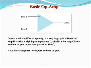
Operationalamplifier or op-amp, is a very high gain differential
amplifier with a high input impedance (typically a few meg-Ohms)
and low output impedance (less than 100 ).
Note the op-amp has two inputs and one output.
1
1
2.
Op-Amp Gain
Op-Amp Gain
Op-Ampshave a very high gain. They can be connected open-loop or
closed-loop.
• Open-loop
Open-loop refers to a configuration where there is no feedback
from output back to the input. In the open-loop configuration
the gain can exceed 10,000.
• Closed-loop
Closed-loop configuration reduces the gain. In order to control
the gain of an op-amp it must have feedback. This feedback is a
negative feedback. A negative feedback
negative feedback reduces the gain and
improves many characteristics of the op-amp.
2
2
3.
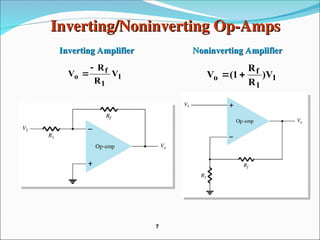
Inverting Op-Amp
Inverting Op-Amp
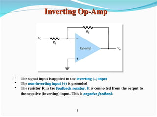
•The signal input is applied to the inverting (–) input
inverting (–) input
• The non-inverting input (+)
non-inverting input (+) is grounded
• The resistor Rf is the feedback resistor
feedback resistor. It is connected from the output to
the negative (inverting) input. This is negative feedback
negative feedback.
3
3
4.
Inverting Op-Amp Gain
InvertingOp-Amp Gain
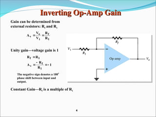
Gain can be determined from
external resistors: Rf and R1
Unity gain—voltage gain is 1
The negative sign denotes a 180
phase shift between input and
output.
1
f
i
o
v
R
R
V
V
A
1
R
R
A
R
R
1
f
v
1
f
Constant Gain—Rf is a multiple of R1
4
4
5.
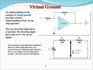
Virtual Ground
Virtual Ground
Anunderstanding of the
concept of virtual ground
virtual ground
provides a better
understanding of how an op-
amp operates.
The non-inverting input pin is
at ground. The inverting input
pin is also at 0 V for an AC
signal.
The op-amp has such high input impedance
that even with a high gain there is no
current from inverting input pin, therefore
there is no voltage from inverting pin to
ground—all of the current is through Rf.
5
5
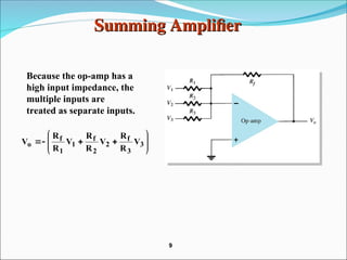
Summing Amplifier
Summing Amplifier
Becausethe op-amp has a
high input impedance, the
multiple inputs are
treated as separate inputs.
3
3
f
2
2
f
1
1
f
o V
R
R
V
R
R
V
R
R
V
9
9
10.
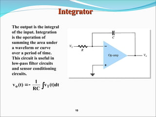
Integrator
Integrator
The output isthe integral
of the input. Integration
is the operation of
summing the area under
a waveform or curve
over a period of time.
This circuit is useful in
low-pass filter circuits
and sensor conditioning
circuits.
(t)dt
v
RC
1
(t)
v 1
o
10
10
Op-Amp Specifications—DC Offset
Op-AmpSpecifications—DC Offset
Parameters
Parameters
• Input offset voltage
• Input offset current
• Input offset voltage and input offset current
• Input bias current
Even when the input voltage is zero, there can be an
output offset
offset. The following can cause this offset:
12
12
13.
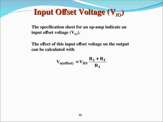
Input Offset Voltage(V
Input Offset Voltage (VIO
IO)
)
The specification sheet for an op-amp indicate an
input offset voltage (VIO).
The effect of this input offset voltage on the output
can be calculated with
1
f
1
IO
o(offset)
R
R
R
V
V
13
13
14.
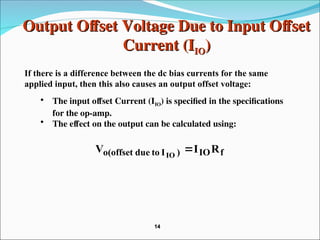
Output Offset VoltageDue to Input Offset
Output Offset Voltage Due to Input Offset
Current (I
Current (IIO
IO)
)
• The input offset Current (IIO) is specified in the specifications
for the op-amp.
• The effect on the output can be calculated using:
f
IO
)
I
to
due
o(offset R
I
V IO
If there is a difference between the dc bias currents for the same
applied input, then this also causes an output offset voltage:
14
14
15.
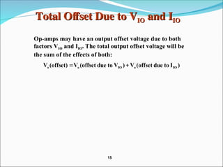
Total Offset Dueto V
Total Offset Due to VIO
IO and I
and IIO
IO
Op-amps may have an output offset voltage due to both
factors VIO and IIO. The total output offset voltage will be
the sum of the effects of both:
)
I
to
due
(offset
V
)
V
to
due
(offset
V
(offset)
V IO
o
IO
o
o
15
15
16.
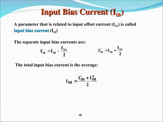
Input Bias Current(I
Input Bias Current (IIB
IB)
)
A parameter that is related to input offset current (IIO) is called
input bias current
input bias current (IIB)
The separate input bias currents are:
The total input bias current is the average:
2
I
I
I IO
IB
IB
2
I
I
I IO
IB
IB
2
I
I
I IB
IB
IB
16
16
17.
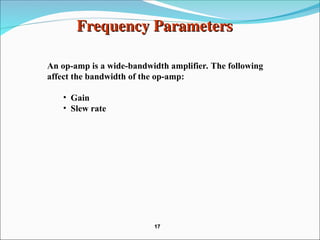
An op-amp isa wide-bandwidth amplifier. The following
affect the bandwidth of the op-amp:
• Gain
• Slew rate
Frequency Parameters
Frequency Parameters
17
17
18.
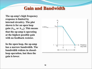
Gain and Bandwidth
Gainand Bandwidth
The op-amp’s high frequency
response is limited by
internal circuitry. The plot
shown is for an open loop
gain (AOL or AVD). This means
that the op-amp is operating
at the highest possible gain
with no feedback resistor.
In the open loop, the op-amp
has a narrow bandwidth. The
bandwidth widens in closed-
loop operation, but then the
gain is lower.
18
18
19.
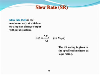
Slew Rate (SR)
SlewRate (SR)
Slew rate (SR)
Slew rate (SR) is the
maximum rate at which an
op-amp can change output
without distortion.
The SR rating is given in
the specification sheets as
V/s rating.
s)
V/
(in
Δt
ΔV
SR o
19
19
20.
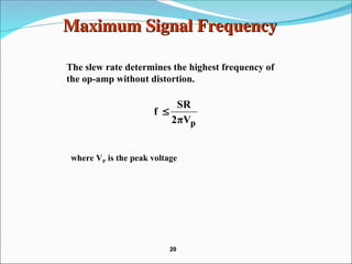
Maximum Signal Frequency
MaximumSignal Frequency
The slew rate determines the highest frequency of
the op-amp without distortion.
where VP is the peak voltage
p
V
π
2
SR
f
20
20
21.
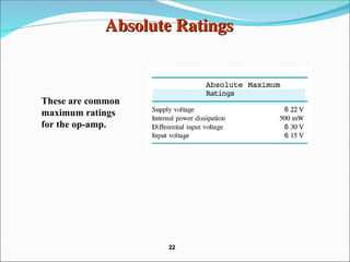
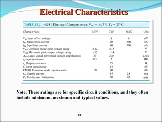
General Op-Amp Specifications
GeneralOp-Amp Specifications
Other ratings for op-amp found on specification sheets
are:
• Absolute Ratings
• Electrical Characteristics
• Performance
21
21
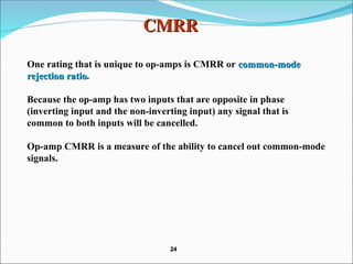
CMRR
CMRR
One rating thatis unique to op-amps is CMRR or common-mode
common-mode
rejection ratio
rejection ratio.
Because the op-amp has two inputs that are opposite in phase
(inverting input and the non-inverting input) any signal that is
common to both inputs will be cancelled.
Op-amp CMRR is a measure of the ability to cancel out common-mode
signals.
24
24
25.
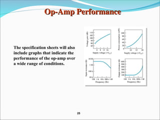
Op-Amp Performance
Op-Amp Performance
Thespecification sheets will also
include graphs that indicate the
performance of the op-amp over
a wide range of conditions.
25
25