Downloaded 61 times


![Example #3 (con’t)
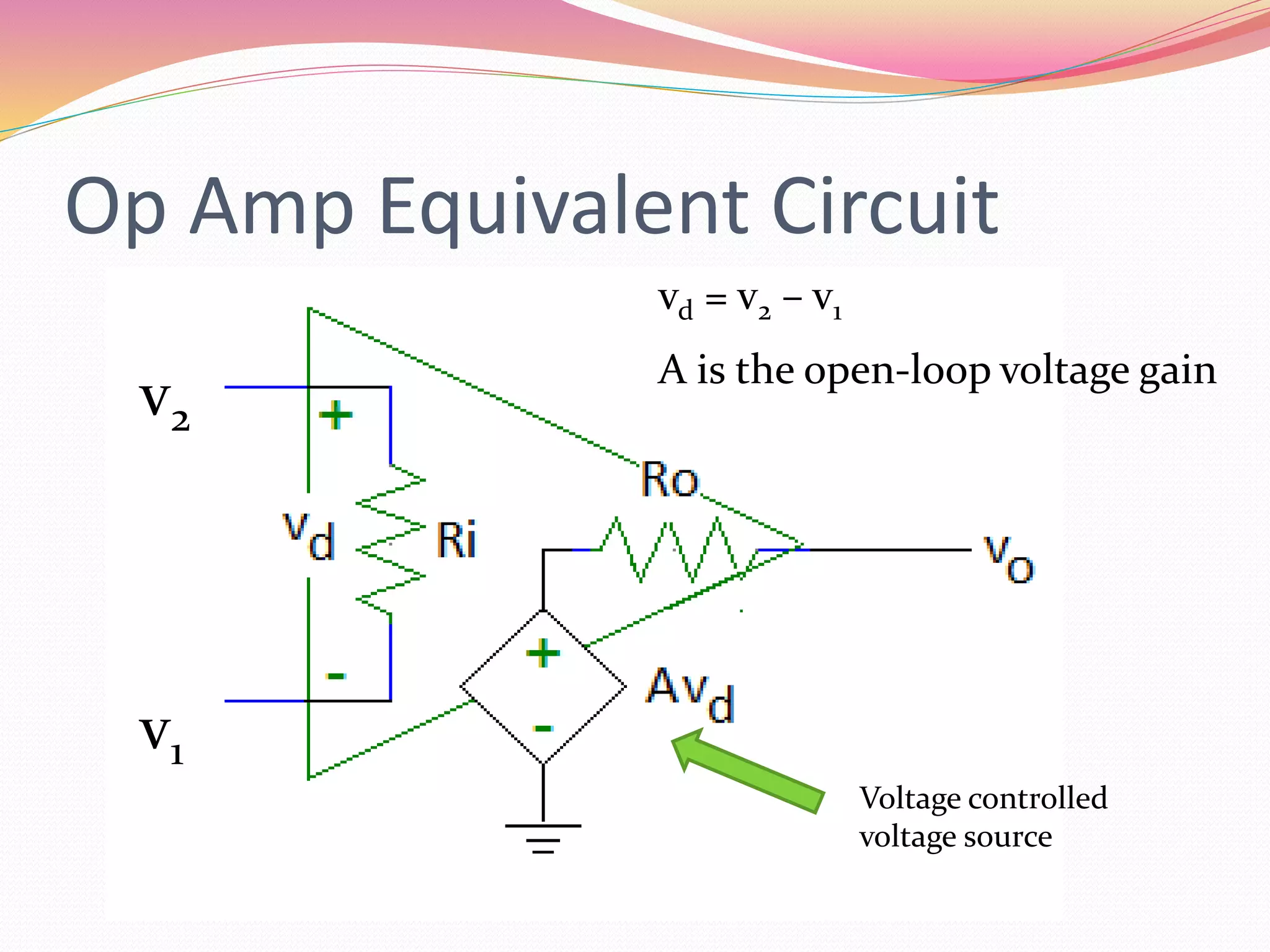
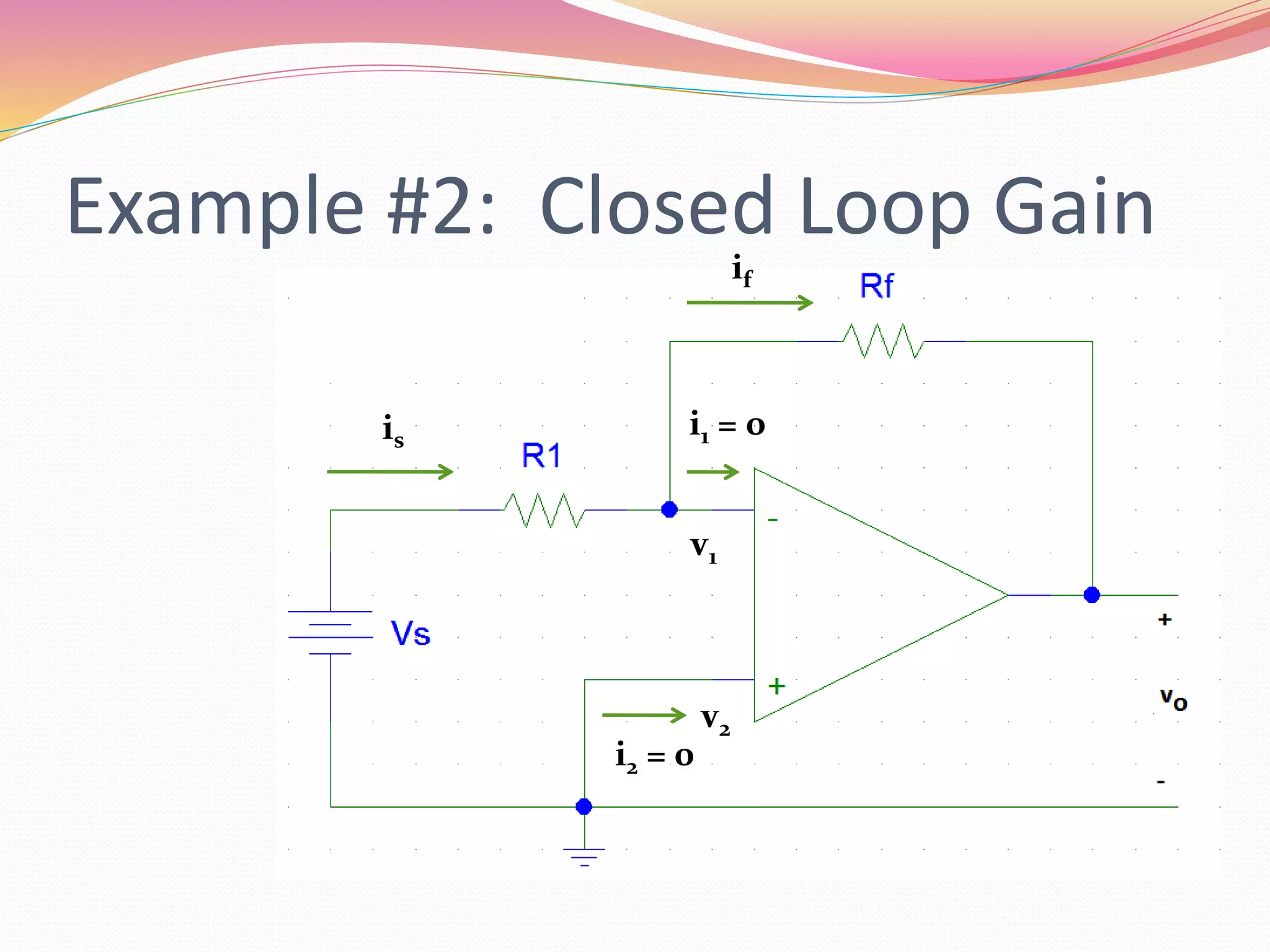
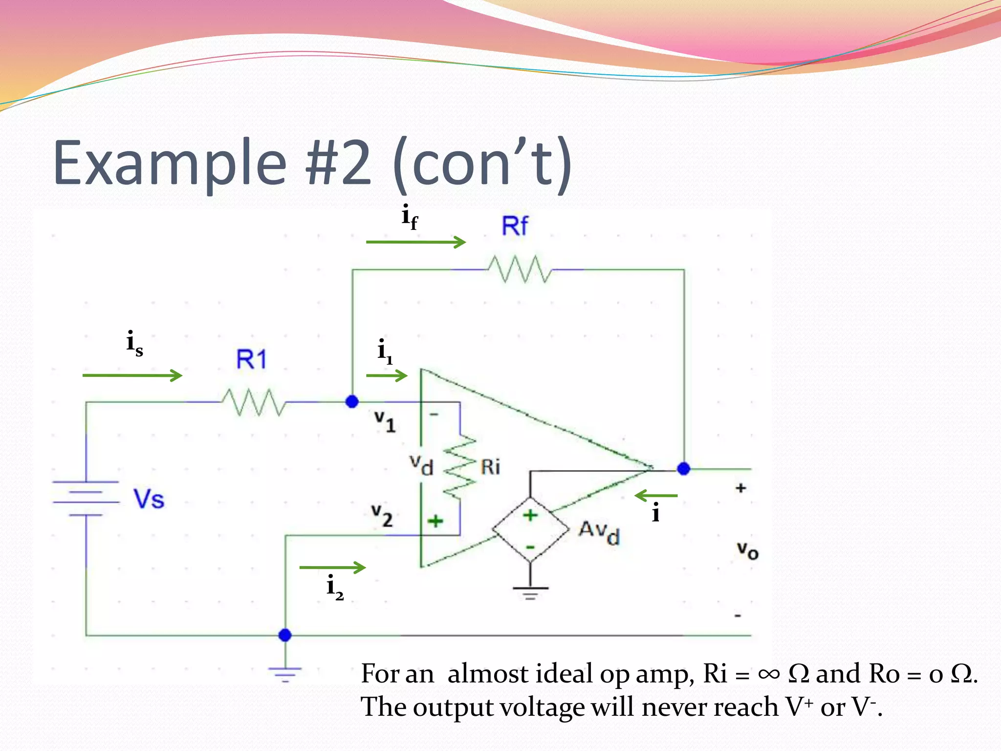
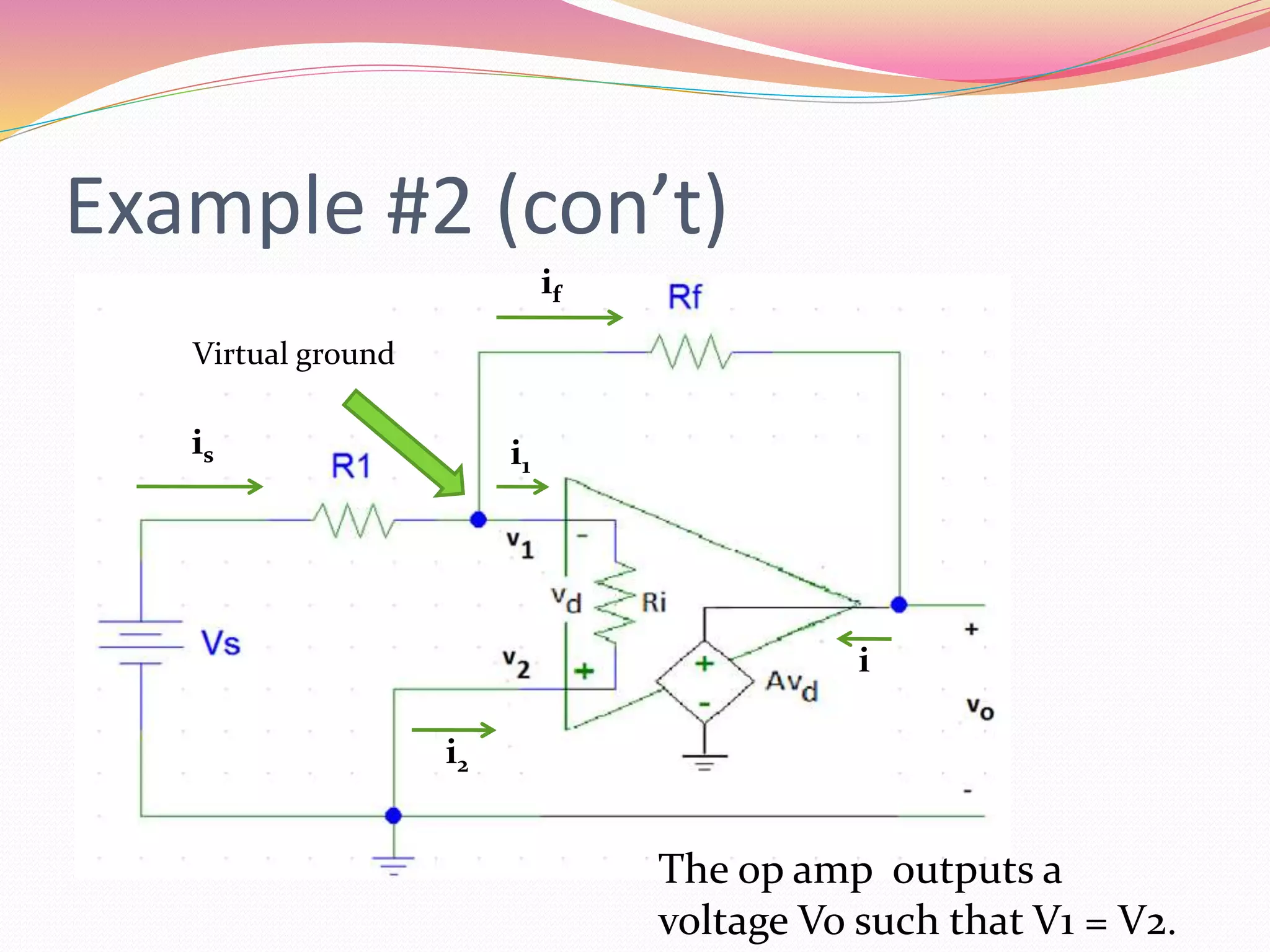
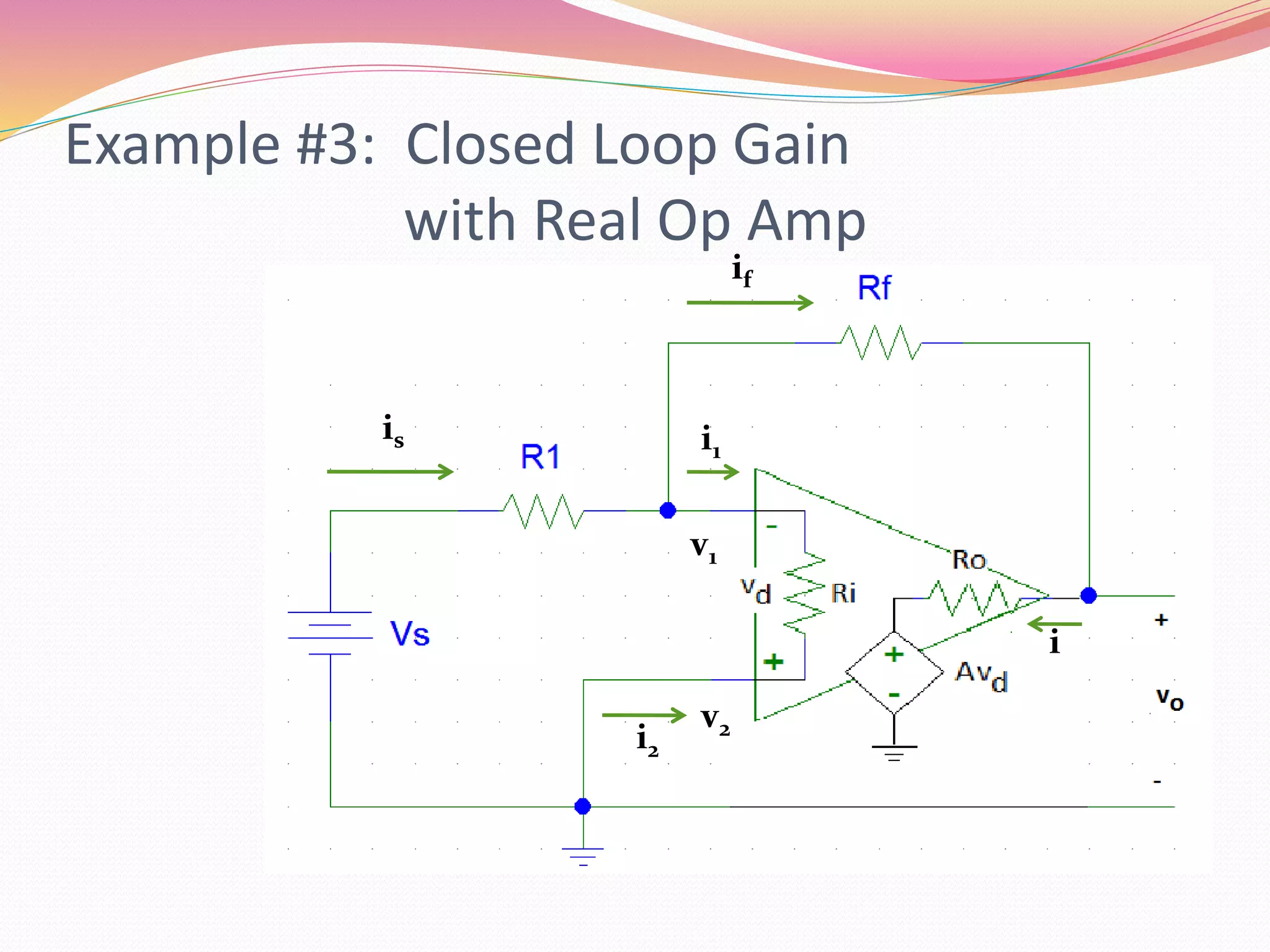
is = i1 + if
i = if
- i1 = i2
vd = v2 – v1 = Ri (- i1) = Ri (i2)
Vo = Avd - Ro(- i)
Vs = R1(is) – vd
Vs = R1(is) + Rf(if) + Vo
Vo /Vs = (-Rf/R1){Ab/[1 +Ab]}, where b = R1/(R1+Rf)](https://image.slidesharecdn.com/z4hsixeq8wbzq7up0cvr-signature-4aa7d94a378fffb4ecb5482841aaed28609995562df1f578fa49773d4cacc280-poli-170324085346/75/Operational-amplifiers-28-2048.jpg)


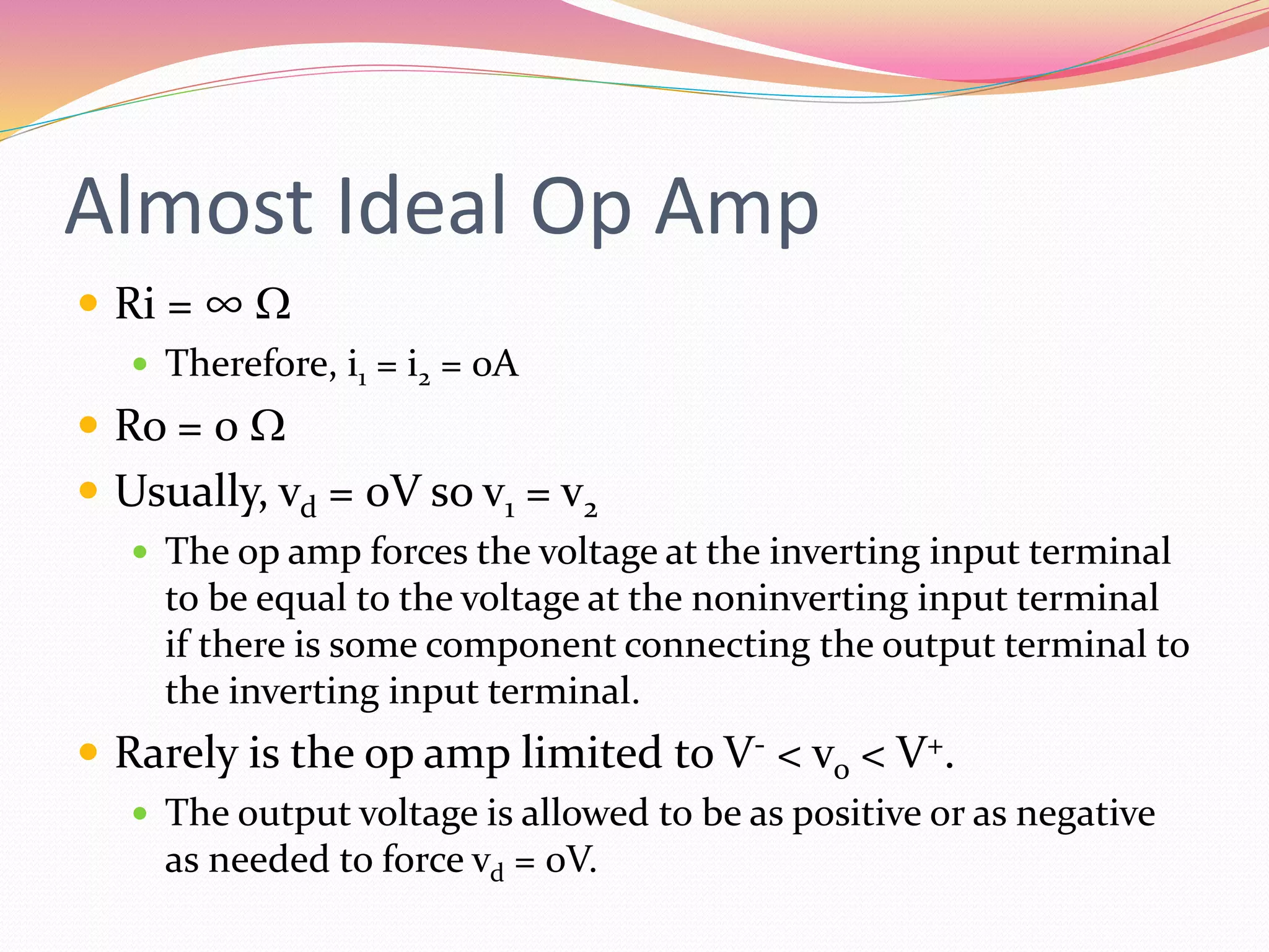
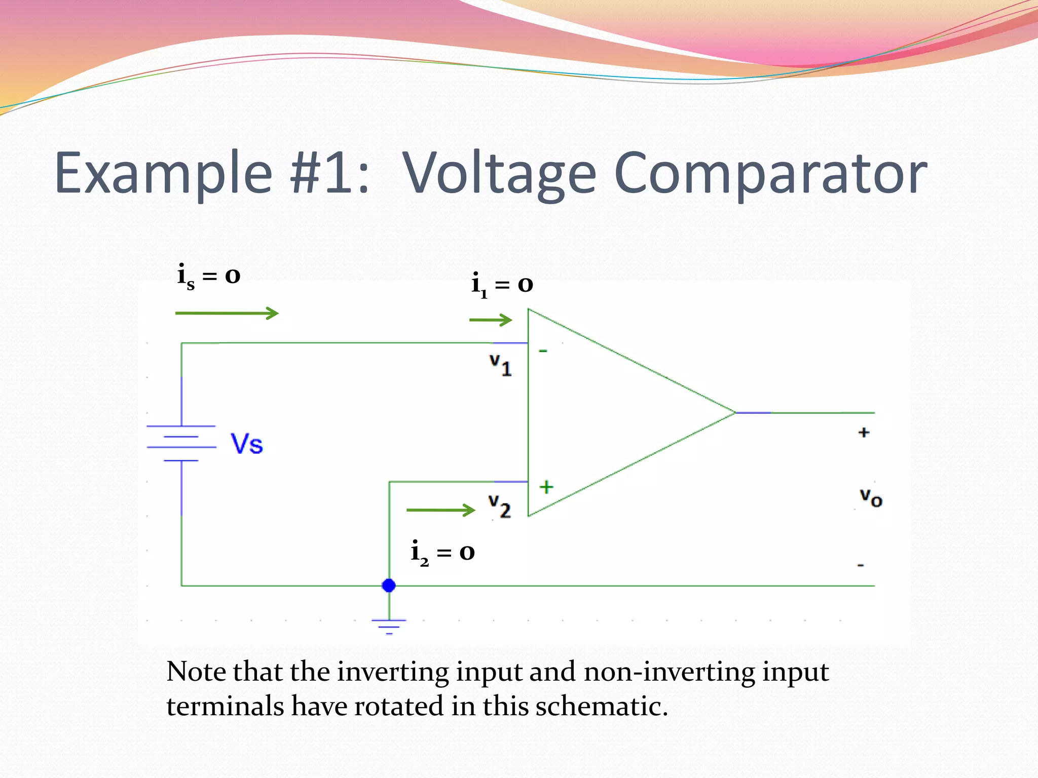
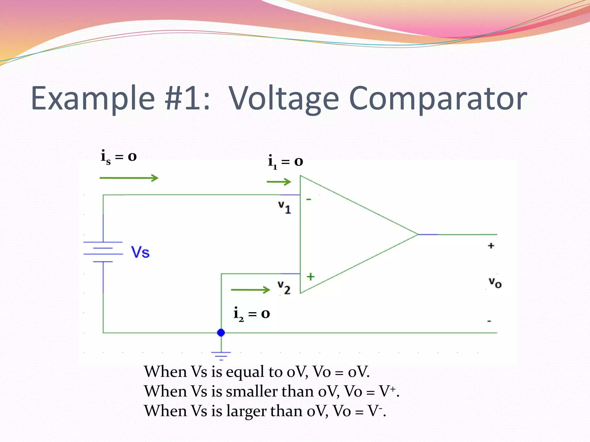
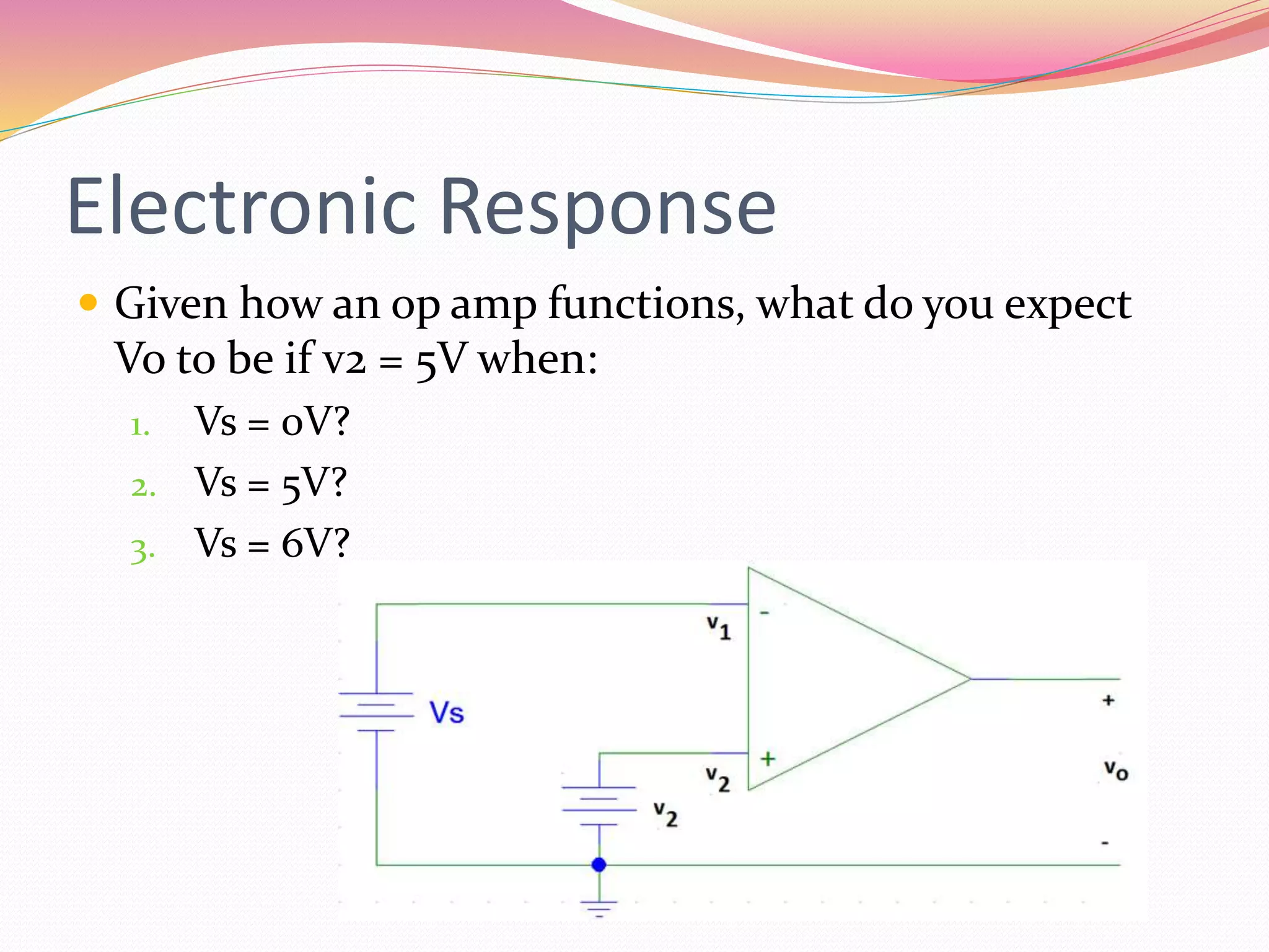
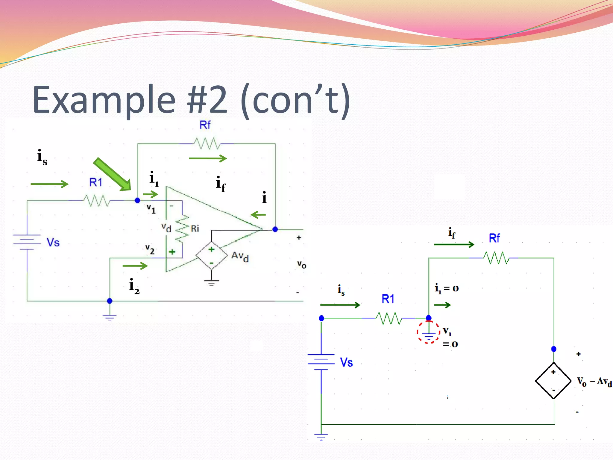
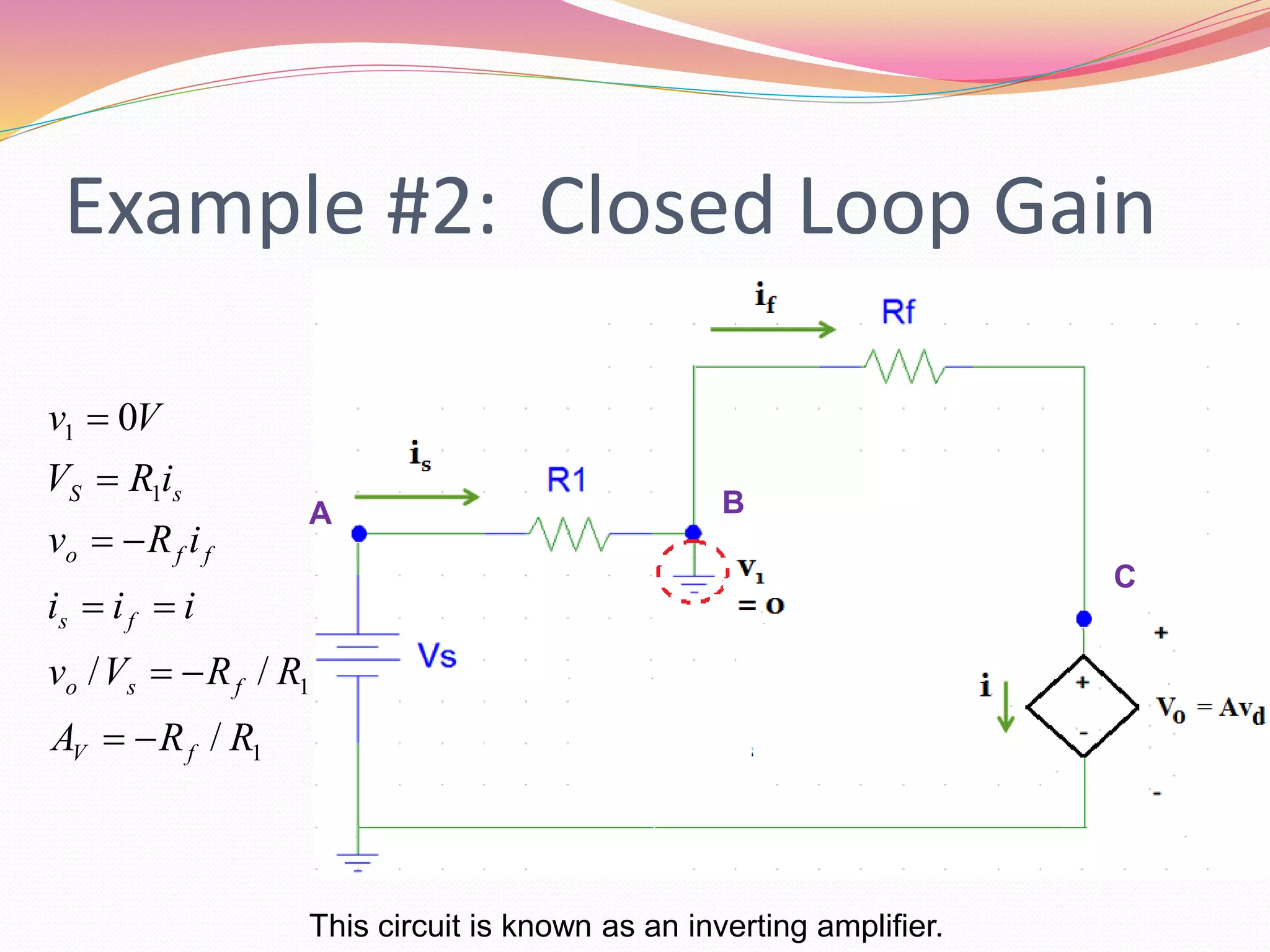
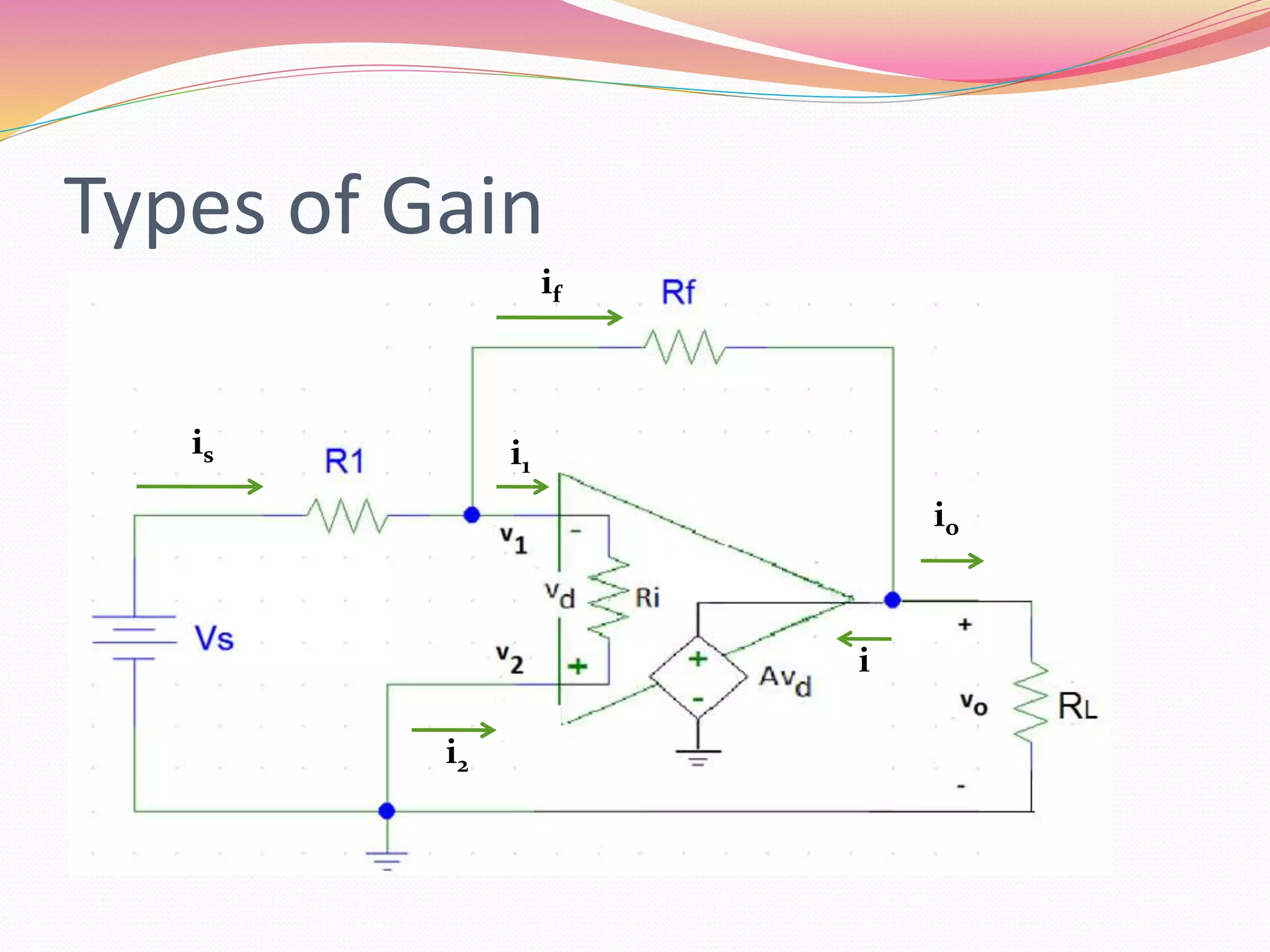
The document discusses operational amplifiers (op amps). It defines key terms like voltage gain and describes how an ideal op amp behaves by forcing its two input terminals to have the same voltage. Real op amps are limited by supply voltages. Example circuits like voltage comparators and inverting amplifiers are analyzed. Gains are defined and the effects of a real op amp having finite input and output resistances are explained.


