Downloaded 75 times

![PLL Control System Block Diagram
With Phase Relationships
θo
θi θi θ0
n mf
[Goldman 2007 p19]
Goldman Technology 1/26/2012 Page 9](https://image.slidesharecdn.com/pllbasiclinkedin2-13276166239432-phpapp01-120126164259-phpapp01/85/Pll-Basic-Linkedin2-9-320.jpg)
![Ideal VCO Transfer Function,
Transduces Voltage to Frequency (Edges)
ωout=ωoff+Kv Vtune ωout=∆θout/∆t
1 E9
8 E8
To = 2 M Td
4 E8
0
[Goldman 2007 p3]
Goldman Technology 1/26/2012 Page 11](https://image.slidesharecdn.com/pllbasiclinkedin2-13276166239432-phpapp01-120126164259-phpapp01/85/Pll-Basic-Linkedin2-11-320.jpg)
![Ideal Phase Detector Transfer Function,
Transduces Frequency (Edge) Differences to Voltage
Vpdavg=Kd θe (5MHz Ref. Freq.)
-200 -100 0 100 200
Ref. – VCO Edge (ns) [Goldman 2007 p2]
Goldman Technology 1/26/2012 Page 14](https://image.slidesharecdn.com/pllbasiclinkedin2-13276166239432-phpapp01-120126164259-phpapp01/85/Pll-Basic-Linkedin2-14-320.jpg)
![Output of Analog Phase Detector vs Phase Error (-cos)
with Various Measures of Abscissa
[Goldman 2007 p18]
Goldman Technology 1/26/2012 Page 15](https://image.slidesharecdn.com/pllbasiclinkedin2-13276166239432-phpapp01-120126164259-phpapp01/85/Pll-Basic-Linkedin2-15-320.jpg)
![Example of Lock, Digital Loop
(In Phase)
[Goldman 2007 p4]
Goldman Technology 1/26/2012 Page 16](https://image.slidesharecdn.com/pllbasiclinkedin2-13276166239432-phpapp01-120126164259-phpapp01/85/Pll-Basic-Linkedin2-16-320.jpg)
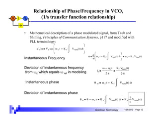
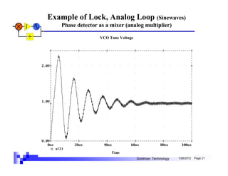
![Mathematical Relationship of Phase and Frequency (Analog Phase Detector)
Phase detector as a mixer (analog multiplier)
Mixing of Two Signals Signal Definition
V1(t) V2(t) = Vp1Vp2 cos(ωrf t + θe ) cos(ωlo t )
V1(t)= Vp1 cos(ωrft+ θe )
where:
Using the trigonometric identity for products of a trigonometric function:
V1(t)= Source 1 signal,
Vp1= Maximum amplitude of source 1 (volts),
V1(t) V2(t)=Vp1Vp2 0.5 [cos ( ωrf t- ωlo t + θe ) +cos( ωrf t + ωlo t + θe )]
ωrf= Angular frequency of a Signal at the RF port of the mixer (rad./sec),
where: = 2 π frf,
V1(t) V2(t) = Mixing process. θe= Phase error difference between signal 1 and 2 (rad.), and
t= Time variable (seconds).
Eliminating the high frequency product V2(t) = Vp2 cos(ωlo t )
with a low pass filter yields where:
V2(t)= Source 2 signal,
V1(t) V2(t) =Vp1 Vp2 0.5 [ cos(ωrf t - ωlo t + θe ) ] Vp2= Maximum amplitude of source 2 (volts), and
ωlo= Angular frequency of a signal at the LO port of a mixer (rad./sec).
=Vpbeat cos( ωbeat t + θe )
where:
ωbeat = ωrf - ωlo for ωrf > ωlo,
Vpbeat = Vp1 Vp2 x 0.5 x mixer losses, and
= The resulting voltage level after mixing (volts).
Slope
V pds
d
( )
V pbeat ⋅cos θ e ( )
V pbeat ⋅sin θ e
dθ e
where:
Vpds ( φ)= Phase detector phase slope (volts).
Phase Detector Gain
Vpds(θe) = Vpbeat sin(θe ) Kd=Vpbeat
Goldman Technology 1/26/2012 Page 17](https://image.slidesharecdn.com/pllbasiclinkedin2-13276166239432-phpapp01-120126164259-phpapp01/85/Pll-Basic-Linkedin2-17-320.jpg)
![Loop Classifications
[Goldman 2007 p8]
Goldman Technology 1/26/2012 Page 19](https://image.slidesharecdn.com/pllbasiclinkedin2-13276166239432-phpapp01-120126164259-phpapp01/85/Pll-Basic-Linkedin2-19-320.jpg)
![Loop Classifications (Continued)
[Goldman 2007 p8]
Goldman Technology 1/26/2012 Page 20](https://image.slidesharecdn.com/pllbasiclinkedin2-13276166239432-phpapp01-120126164259-phpapp01/85/Pll-Basic-Linkedin2-20-320.jpg)
![Judging Stability from Step Response
Freqeuncy (Hz)
6 10 4
.035 Damping
4 deg. Phase Margin 3 10 4
~90% Overshoot
0
4
6 10
.2 Damping
22 deg. Phase Margin 3 10 4
~60% Overshoot
0
4
6 10
.42 Damping 4
45 deg. Phase Margin 3 10
~40% Overshoot
0
0 0.001 0.002 0.003 0.004 0.005 0.006 0.007 0.008 0.009 0.01
Time (s)
[Goldman 2007 p20]
30 deg or 45 deg. Phase Margin are levels supported in references
Goldman Technology 1/26/2012 Page 25](https://image.slidesharecdn.com/pllbasiclinkedin2-13276166239432-phpapp01-120126164259-phpapp01/85/Pll-Basic-Linkedin2-25-320.jpg)
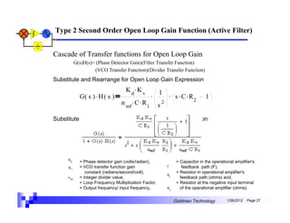
![PLL Basic Block Diagram
For Cascade of Transfer functions for Open Loop Gain
[Goldman 2007 p22]
Goldman Technology 1/26/2012 Page 26](https://image.slidesharecdn.com/pllbasiclinkedin2-13276166239432-phpapp01-120126164259-phpapp01/85/Pll-Basic-Linkedin2-26-320.jpg)
![Loop Stability, Bode Plot
Magnitude
Phase Margin
Phase
Gain Margin
[Goldman 2007 p27]
Goldman Technology 1/26/2012 Page 31](https://image.slidesharecdn.com/pllbasiclinkedin2-13276166239432-phpapp01-120126164259-phpapp01/85/Pll-Basic-Linkedin2-31-320.jpg)
![Graphical Relationship of Natural Frequency to 0 dB Crossover Frequency
[Goldman 2007 p29]
Goldman Technology 1/26/2012 Page 32](https://image.slidesharecdn.com/pllbasiclinkedin2-13276166239432-phpapp01-120126164259-phpapp01/85/Pll-Basic-Linkedin2-32-320.jpg)
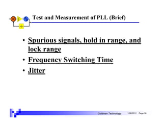
![Spurious Signals
[Goldman 2007 p357]
Goldman Technology 1/26/2012 Page 37](https://image.slidesharecdn.com/pllbasiclinkedin2-13276166239432-phpapp01-120126164259-phpapp01/85/Pll-Basic-Linkedin2-37-320.jpg)
![Hold In Range, Lock In Range
[Goldman 2007 p355]
Goldman Technology 1/26/2012 Page 38](https://image.slidesharecdn.com/pllbasiclinkedin2-13276166239432-phpapp01-120126164259-phpapp01/85/Pll-Basic-Linkedin2-38-320.jpg)
![Jitter, Oscilloscope
[Goldman 2007 p388]
Goldman Technology 1/26/2012 Page 40](https://image.slidesharecdn.com/pllbasiclinkedin2-13276166239432-phpapp01-120126164259-phpapp01/85/Pll-Basic-Linkedin2-40-320.jpg)
![Relationship of Modulation Domain to
Spectrum Analyzer and Oscilloscope
F
T
V
[Goldman 2007 p378]
Goldman Technology 1/26/2012 Page 41](https://image.slidesharecdn.com/pllbasiclinkedin2-13276166239432-phpapp01-120126164259-phpapp01/85/Pll-Basic-Linkedin2-41-320.jpg)
![Oscilloscope Measurement of 1 and Multiple Periods
1 clo ck p eriod oscilloscop e m easurem ent w ith jitter FM m odulation
1 p eriod scope m easurem ent
1
T
1
6 clock periods o scilloscope m easurem ent w ith jitter F M m odulation
6 th period scop e m easurem ent
1
T
1 [Goldman 2007 p380]
Goldman Technology 1/26/2012 Page 42](https://image.slidesharecdn.com/pllbasiclinkedin2-13276166239432-phpapp01-120126164259-phpapp01/85/Pll-Basic-Linkedin2-42-320.jpg)
![Frequency Switching Time, Modulation Domain Analyzer
[Goldman 2007 p358]
Goldman Technology 1/26/2012 Page 43](https://image.slidesharecdn.com/pllbasiclinkedin2-13276166239432-phpapp01-120126164259-phpapp01/85/Pll-Basic-Linkedin2-43-320.jpg)

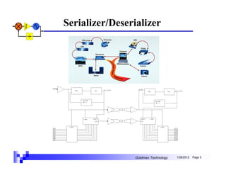
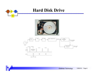
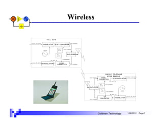
The document provides an overview of phase-locked loops (PLLs), including their history, applications, components, and design requirements. It discusses how PLLs work, beginning with an early use in 1932 for radio signal reception. Key applications include frequency multiplication, modulation/demodulation, data synchronization, and use in devices like cell phones and hard disk drives. Diagrams and equations are provided to illustrate the relationships between phase and frequency in a PLL system and its voltage-controlled oscillator, phase detector, and charge pump components.


![RF Module Design - [Chapter 8] Phase-Locked Loops](https://cdn.slidesharecdn.com/ss_thumbnails/rfch8-150613070348-lva1-app6892-thumbnail.jpg?width=640&height=640&fit=bounds)
![RF Module Design - [Chapter 4] Transceiver Architecture](https://cdn.slidesharecdn.com/ss_thumbnails/rfch4-150613070346-lva1-app6891-thumbnail.jpg?width=640&height=640&fit=bounds)


![Multiband Transceivers - [Chapter 2] Noises and Linearities](https://cdn.slidesharecdn.com/ss_thumbnails/ch2-150613070933-lva1-app6892-thumbnail.jpg?width=640&height=640&fit=bounds)


