Presentation 
On 
Unipolar 
BY: Roshan Chaudhary (13ITU031)
Unipolar 
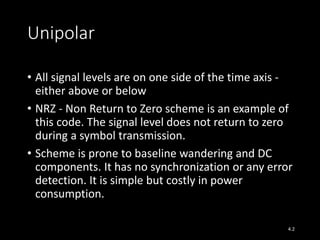
• All signal levels are on one side of the time axis - 
either above or below 
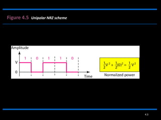
• NRZ - Non Return to Zero scheme is an example of 
this code. The signal level does not return to zero 
during a symbol transmission. 
• Scheme is prone to baseline wandering and DC 
components. It has no synchronization or any error 
detection. It is simple but costly in power 
consumption. 
4.2
4.3 
Figure 4.5 Unipolar NRZ scheme
Unipolar Signalling 
Unipolar Non-Return to Zero (NRZ): 
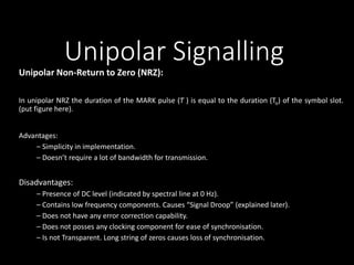
In unipolar NRZ the duration of the MARK pulse (Ƭ ) is 
equal to the duration (To) of the symbol slot. 
1 0 1 0 1 1 1 1 1 0 
V 
0
Unipolar Signalling 
Unipolar Non-Return to Zero (NRZ): 
In unipolar NRZ the duration of the MARK pulse (Ƭ ) is equal to the duration (To) of the symbol slot. 
(put figure here). 
Advantages: 
– Simplicity in implementation. 
– Doesn’t require a lot of bandwidth for transmission. 
Disadvantages: 
– Presence of DC level (indicated by spectral line at 0 Hz). 
– Contains low frequency components. Causes “Signal Droop” (explained later). 
– Does not have any error correction capability. 
– Does not posses any clocking component for ease of synchronisation. 
– Is not Transparent. Long string of zeros causes loss of synchronisation.
Unipolar Signalling 
Unipolar Non-Return to Zero (NRZ): 
Figure. PSD of Unipolar NRZ
Unipolar Signalling 
Return to Zero (RZ): 
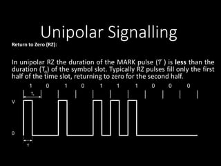
In unipolar RZ the duration of the MARK pulse (Ƭ ) is less than the 
duration (To) of the symbol slot. Typically RZ pulses fill only the first 
half of the time slot, returning to zero for the second half. 
1 0 1 0 1 1 1 0 0 0 
V 
0 
To 
Ƭ
Unipolar Signalling 
Return to Zero (RZ): 
In unipolar RZ the duration of the MARK pulse (Ƭ ) is less than the duration (To) of the symbol slot. Typically RZ 
pulses fill only the first half of the time slot, returning to zero for the second half. 
1 0 1 0 1 1 1 0 0 0 
V 
0 
To 
Ƭ
Unipolar Signalling 
Unipolar Return to Zero (RZ): 
Advantages: 
– Simplicity in implementation. 
– Presence of a spectral line at symbol rate which can be used as symbol 
timing clock signal. 
Disadvantages: 
– Presence of DC level (indicated by spectral line at 0 Hz). 
– Continuous part is non-zero at 0 Hz. Causes “Signal Droop”. 
– Does not have any error correction capability. 
– Occupies twice as much bandwidth as Unipolar NRZ. 
– Is not Transparent
Unipolar Signalling 
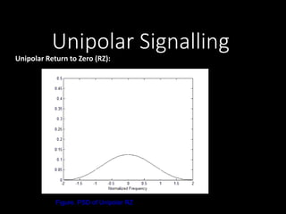
Unipolar Return to Zero (RZ): 
Figure. PSD of Unipolar RZ
Unipolar Signalling 
In conclusion it can be said that neither variety of 
unipolar signals is suitable for transmission over AC 
coupled lines.
UNIPOLAR LOGIC FAMILIES 
• MOS devices are unipolar devices and only 
MOSFETs are employed in MOS logic circuits. 
• These families are: 
• PMOS (p-channel MOSFETs) 
• NMOS (n-channel MOSFETs) 
• CMOS (Both p- and n- channel MOSFETs 
are fabricated on same silicon chip)
MOS 
• Unipolar transistor depends on only one 
type of carrier. 
• Carrier may be electrons or holes. 
• Used in Lsi & vlsi 
• Metal electrode is placed on top of oxide 
insulator ie the semiconductor material. 
• Mosfet is used where power consumption is 
low.
PMOS,NMOS,CMOS 
• P channel mos is referred as pmos. 
• P oldest and slowest obsolete. 
• Nmos n channel and used in circuits with one type 
of MOS transistor. 
• Nmos used in microprocessor and memories. 
• CMOS combination n and p channel. 
• Cmos is also explained as “Complementary – 
Symmetry”. 
• Cmos uses Symmetrical pairs of electronic 
devices p type and n type.
Characteristics of Cmos 
• High input resistance. 
• Compatible output of one device can be 
connected to another CMOS. 
• High noise immunity 
• Low static power 
• High density on chip 
• Simple 
• Protection circuitry 
• Absorb electric charges with no damage.
Usage Cmos 
• Microcontrollers, microprocessor, RAM 
• Image sensors, data converter and integrated 
transceivers and other types of communication. 
• Current IBM mainframes . 
• Digital wristwatches, calculators and portable 
computers. 
ADVANTAGE 
Dissipate less power . 
Operates on high speed. 
Low cost 
More economical operation
COMPARISONS TTL,ECL,CMOS 
TTL 
ECL 
Cmos 
Power consumption 
increase with clock 
speed 
Power consumption is 
high 
Power consumption does 
not increase 
Less sensitive 
elecrostatic discharge 
More sensitive electrostatic 
discharge 
Nand gate Nor gate Not gate 
Provides more heat 
cos power dissipation 
is more

Unipolar

  • 1.
    Presentation On Unipolar BY: Roshan Chaudhary (13ITU031)
  • 2.
    Unipolar • Allsignal levels are on one side of the time axis - either above or below • NRZ - Non Return to Zero scheme is an example of this code. The signal level does not return to zero during a symbol transmission. • Scheme is prone to baseline wandering and DC components. It has no synchronization or any error detection. It is simple but costly in power consumption. 4.2
  • 3.
    4.3 Figure 4.5Unipolar NRZ scheme
  • 4.
    Unipolar Signalling UnipolarNon-Return to Zero (NRZ): In unipolar NRZ the duration of the MARK pulse (Ƭ ) is equal to the duration (To) of the symbol slot. 1 0 1 0 1 1 1 1 1 0 V 0
  • 5.
    Unipolar Signalling UnipolarNon-Return to Zero (NRZ): In unipolar NRZ the duration of the MARK pulse (Ƭ ) is equal to the duration (To) of the symbol slot. (put figure here). Advantages: – Simplicity in implementation. – Doesn’t require a lot of bandwidth for transmission. Disadvantages: – Presence of DC level (indicated by spectral line at 0 Hz). – Contains low frequency components. Causes “Signal Droop” (explained later). – Does not have any error correction capability. – Does not posses any clocking component for ease of synchronisation. – Is not Transparent. Long string of zeros causes loss of synchronisation.
  • 6.
    Unipolar Signalling UnipolarNon-Return to Zero (NRZ): Figure. PSD of Unipolar NRZ
  • 7.
    Unipolar Signalling Returnto Zero (RZ): In unipolar RZ the duration of the MARK pulse (Ƭ ) is less than the duration (To) of the symbol slot. Typically RZ pulses fill only the first half of the time slot, returning to zero for the second half. 1 0 1 0 1 1 1 0 0 0 V 0 To Ƭ
  • 8.
    Unipolar Signalling Returnto Zero (RZ): In unipolar RZ the duration of the MARK pulse (Ƭ ) is less than the duration (To) of the symbol slot. Typically RZ pulses fill only the first half of the time slot, returning to zero for the second half. 1 0 1 0 1 1 1 0 0 0 V 0 To Ƭ
  • 9.
    Unipolar Signalling UnipolarReturn to Zero (RZ): Advantages: – Simplicity in implementation. – Presence of a spectral line at symbol rate which can be used as symbol timing clock signal. Disadvantages: – Presence of DC level (indicated by spectral line at 0 Hz). – Continuous part is non-zero at 0 Hz. Causes “Signal Droop”. – Does not have any error correction capability. – Occupies twice as much bandwidth as Unipolar NRZ. – Is not Transparent
  • 10.
    Unipolar Signalling UnipolarReturn to Zero (RZ): Figure. PSD of Unipolar RZ
  • 11.
    Unipolar Signalling Inconclusion it can be said that neither variety of unipolar signals is suitable for transmission over AC coupled lines.
  • 12.
    UNIPOLAR LOGIC FAMILIES • MOS devices are unipolar devices and only MOSFETs are employed in MOS logic circuits. • These families are: • PMOS (p-channel MOSFETs) • NMOS (n-channel MOSFETs) • CMOS (Both p- and n- channel MOSFETs are fabricated on same silicon chip)
  • 13.
    MOS • Unipolartransistor depends on only one type of carrier. • Carrier may be electrons or holes. • Used in Lsi & vlsi • Metal electrode is placed on top of oxide insulator ie the semiconductor material. • Mosfet is used where power consumption is low.
  • 14.
    PMOS,NMOS,CMOS • Pchannel mos is referred as pmos. • P oldest and slowest obsolete. • Nmos n channel and used in circuits with one type of MOS transistor. • Nmos used in microprocessor and memories. • CMOS combination n and p channel. • Cmos is also explained as “Complementary – Symmetry”. • Cmos uses Symmetrical pairs of electronic devices p type and n type.
  • 16.
    Characteristics of Cmos • High input resistance. • Compatible output of one device can be connected to another CMOS. • High noise immunity • Low static power • High density on chip • Simple • Protection circuitry • Absorb electric charges with no damage.
  • 18.
    Usage Cmos •Microcontrollers, microprocessor, RAM • Image sensors, data converter and integrated transceivers and other types of communication. • Current IBM mainframes . • Digital wristwatches, calculators and portable computers. ADVANTAGE Dissipate less power . Operates on high speed. Low cost More economical operation
  • 19.
    COMPARISONS TTL,ECL,CMOS TTL ECL Cmos Power consumption increase with clock speed Power consumption is high Power consumption does not increase Less sensitive elecrostatic discharge More sensitive electrostatic discharge Nand gate Nor gate Not gate Provides more heat cos power dissipation is more