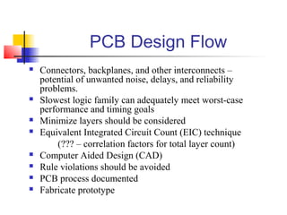
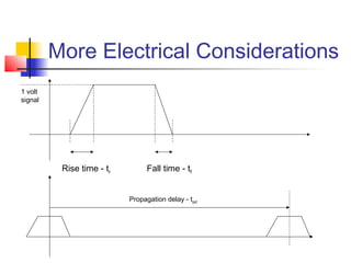
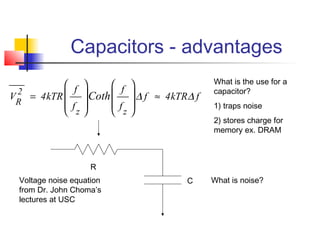
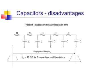
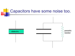
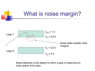
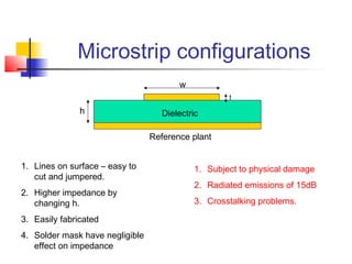
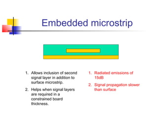
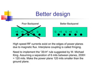
SlideShare a Scribd company logo
1 of 30
High Performance Printed
     Circuit Boards

     By Joseph Y. Lee
 Samsung Electro-Mechanics
Chapter – 6

    Design of
High Performance
  Circuit Boards
PCB Design Flow
   Connectors, backplanes, and other interconnects –
    potential of unwanted noise, delays, and reliability
    problems.
   Slowest logic family can adequately meet worst-case
    performance and timing goals
   Minimize layers should be considered
   Equivalent Integrated Circuit Count (EIC) technique
         (??? – correlation factors for total layer count)
   Computer Aided Design (CAD)
   Rule violations should be avoided
   PCB process documented
   Fabricate prototype
Mechanical Design and PCB
Materials
   Printed circuit board sizes
   Board thickness
   Panel sizes (more than one PCB size)
   Mechanical partitioning (ex. space for components
    and cable routing)
   Mechanical support
   Thermal analysis
   Mechanical Interface Control Drawing (relates the
    mechanical chassis constraints to the board
    connector constraints)
   PCB Materials (considerations – mechanical,
    electrical, chemical, thermal)
Electrical Considerations
   Impedance – capacitance, resistance, and
    inductance
   Cross talk; a phenomenon where a signal on
    one line/trace is capacitively coupled to an
    adjacent line/trace. It can be a form or noise.
   Heat; another form of noise – 1.5*kT
   Switching (on-off-on-off) noise; increases while
    impedance decreases. Higher impedance MAY
    solve problem.
More Electrical Considerations
1 volt
signal


          Rise time - tr        Fall time - tf


                           Propagation delay - tpd
Capacitors - advantages
          f      f                       What is the use for a
 2                                           capacitor?
V = 4kTR   Coth         ∆ f ≈ 4kTR ∆ f
 R        f      f                       1) traps noise
          z      z     
                                             2) stores charge for
                                             memory ex. DRAM


                    R
 Voltage noise equation                C     What is noise?
 from Dr. John Choma’s
 lectures at USC
Capacitors - disadvantages
      Tradeoff – capacitors slow propagation time


R          R             R               R         R


          C             C                C         C   C


               Propagation delay - tpd


    tpd = 15 RC for 5 capacitors and 5 resistors
Capacitors have some noise too.


dielectric                 parasitic
                           resistor
What is noise margin?

                                      VOH = 1 V
Logic 1
                                      VIH = 0.8 V

                                                    Noise spike outside noise
                                                    margins
                                      VIL = 0.2 V
Logic 0
                                      VOL= 0 V


          Noise tolerance is the degree to which a gate is impervious to
          noise spikes at its input.
Microstrip configurations
                                        w
                                                    t

               h                    Dielectric

                                 Reference plant


1. Lines on surface – easy to               1. Subject to physical damage
   cut and jumpered.
                                            2. Radiated emissions of 15dB
2. Higher impedance by
   changing h.                              3. Crosstalking problems.

3. Easily fabricated
4. Solder mask have negligible
   effect on impedance
Embedded microstrip


1. Allows inclusion of second    1. Radiated emissions of
   signal layer in addition to      15dB
   surface microstrip.
                                 2. Signal propagation slower
2. Helps when signal layers         than surface
   are required in a
   constrained board
   thickness.
Strip-line


1. Exhibit less cross-talk          1. Difficult to repair or rework
2. Better impedance control         2. Slower propagation time
Dual strip line
                               Reference plane


                               Reference plane


1. Maximizes interconnection               1. Results in very high layer to
   density                                    layer coupling.
2. Routed perpendicularly to               2. Impedance will be lower for
   reduce cross talk.                         dual strip line signal trace
                                              closer to reference plane
                                              compared to strip line signal
                                              trace in the center to the
                                              reference plane.
Cross-talk

   Mutual capacitive and inductive b/t signal
    lines produces cross-talk.
   Moving ground plane closer to signal lines
    reduces cross-talk.
   Forward cross-talk (IL - IC) – normally opposite
    of signal source
   Backward cross-talk (IC + IL) – same as signal
    course, twice the line delay (worst case)
Cross-talk control
   Full or partial termination reduce cross-talk amplitudes.
   Signals must be routed orthogonally.
   Void parallel of high speed logic parallel to low level
    analog circuits.
   Keep all buses physically separate from clocks and
    strobes.
   Distance separation between critical traces must be
    three times the width of the traces measured from
    centerline to centerline.
   Thin traces reduce cross-talk.
   Separate traces at 2 mils/inch of trace length.
   Keep lines short!
Clock and strobe distribution
   Use point to point clock configurations.
   Centrally locate the clock drivers.
   Avoid branching.
   Make clocks, strobes, and control signals first
    priority.
   Do not use the same buffer to drive on and off
    the card simultaneously.
   Do not assign clocks of different frequencies
    to the same clock driver package.
Series termination

   Series termination does not increase
    power dissipation.
   Low state reflections are more
    critical compared to high state
    reflections.
   Must be lumped very close to the
    end of the lines
Parallel termination
                Purpose:

                1. Reduces reflections from ends of the bus.
                2. Provides high state pull-up for open collector
                   drivers.
                3. Provides discharge path for the line when 3-state
                   devices are disabled.
                4. Allows it to put a larger initial voltage step into
Signal line
                   the line on positive transitions.
                Guidelines:
                1. 0.1µF capacitors should be placed as close as
                   possible to Vcc pin.
                2. Choose types that give access to the individual
                   resistor lead since they afford better grounding.
Parallel termination
   Signals travel relatively undistorted.
   Loading delay is about half that of
    series termination.
   Helps to offset the driver versus line
    voltage divider delay
   Higher power consumption.
   Higher cross-talk levels.
   Decreases the low level noise margins.
Differential signal topologies
  Strip-line structure                                   Dual strip-line structure

           Odd-mode coupling      Even-mode coupling             Even-mode coupling


                                         Odd-mode coupling


Coplanar differential structure                        Broadside differential structure


               Even-mode coupling is for digital applications.
Coplanar vs. Broadside
   Odd mode coupling is easier to control with the strip
    line approach than the dual-strip line.
   Less dielectric to achieve desired impedance for
    coplaner.
   Dielectric loss is higher for broadside.
   Common-mode noise is rejected in the coplanar
    approach while it is inherently introduced in the
    broadside configuration.
   Vias are required for broadside to control common
    mode noise.
Net layout guidelines
   Make critical signals first priority.
   Keep signal lines short.
   Use slowest logic family meeting timing requirements.
   Terminate transmission lines.
   Keep loading along distributed nets equal and well balanced.
   Avoid branching.
   Avoid driving on and off card simultaneously.
   Keep stubs off of transmission lines <2 inch.
   Proper grounding practices mandatory.
   When logic devices have risetimes of 1 ns or less, use 45° instead of
    right anges in circuit paths.
   Avoid long test point circuit traces.
   Testability should also be considered.
Definitions
   Ground shifts; difference in ground current
   Backplane; A circuit board containing sockets into
    which other circuit boards can be plugged in.
   EMI; Any electromagnetic disturbance that interrupts,
    obstructs, or otherwise degrades or limits the effective
    performance of electronics/electrical equipment.

      R         R           R         R        R


           Ig         Ig         Ig       Ig       Ig
Reducing ground shifts
   Do not use thermal relief “butterflies.”
   Use the appropriate connectors. Used as
    many ground pins per connector.
   Logic cards that represent the heaviest current
    drain should be located nearest the end where
    the ground enters the backplane.
   Cards with the most single-ended logic
    interconnects between them should be
    assigned to slots as close together as
    possible.
   Consider differential driving.
Multilayer power distribution
   Keep plane spacing as close as possible.
   Multiple 1-oz planes arranged in couplets are
    recommended for distributing backplane power.
   Shorter pins will have less resistance.
   Stagger power/ground inputs on the backplane so as
    to distribute power more evenly into the plane.
   Keep power supply as close as possible to the
    backplane to minimize voltage drops in connecting
    planes.
   2% maximum voltage drop from supplies to any circuit
    device is recommended.
   Use additional planes to distribute auxiliary power in
    the backplane.
Better design
       Poor Backpanel                    Better Backpanel


  +5   +5   G   G   G               G   +5   G +5     G


High speed RF currents exist on the edges of power planes
due to magnetic flux. Interplane coupling is called fringing.
Need to implement the “20-H” rule suggested by W. Michael
King. Assuming a separation of 6 mils between planes, 20XH
= 120 mils. Make the power plane 120 mils smaller than the
ground plane.
Types of capacitors
   NPO – “temperature compensating”
    materials. Capacitance change +/- 0.3% from
    -55 to +125°C.
   X7R – “temperature stable” Capacitance
    change +/- 15% from -55 to +125°C.
   Z5U – “general purpose” provide highest
    capacitance – very unstable under
    environmental changes – small size, low ESL,
    low ESR, and excellent frequency response.
EMI layout guidelines
   Use multilayer boards with dedicated power and
    ground planes.
   Strip-lines reduced radiated emissions up to 15 dB.
   Auxiliary power or ground traces are required – keep
    them as wide as possible to lower inductance and DC
    resistance.
   Adequate decoupling reduces current inductive traces
    and thus lowers emissions.
   Keep highest speed logic closer to the card connector.
   Keep signal traces as short as possible.
   If a noisy card is anticipated, use a strip-line approach.
감사합니다

More Related Content

What's hot

A view of semiconductor industry
A view of semiconductor industryA view of semiconductor industry
A view of semiconductor industryLen Mei
 
High Performance Printed Circuit Boards - Lecture #1
High Performance Printed Circuit Boards - Lecture #1High Performance Printed Circuit Boards - Lecture #1
High Performance Printed Circuit Boards - Lecture #1Samsung Electro-Mechanics
 
5.1주제 용접 품질 기준과 검사 (문흥식)
5.1주제 용접 품질 기준과 검사 (문흥식)5.1주제 용접 품질 기준과 검사 (문흥식)
5.1주제 용접 품질 기준과 검사 (문흥식)topshock
 
Michael john sebastian smith application-specific integrated circuits-addison...
Michael john sebastian smith application-specific integrated circuits-addison...Michael john sebastian smith application-specific integrated circuits-addison...
Michael john sebastian smith application-specific integrated circuits-addison...Đình Khanh Nguyễn
 
Changchun CCP PBT Overview Presentation
Changchun CCP PBT Overview PresentationChangchun CCP PBT Overview Presentation
Changchun CCP PBT Overview PresentationJames Smithson
 
finfet & dg-fet technology
finfet & dg-fet technologyfinfet & dg-fet technology
finfet & dg-fet technologyKritika Ramesh
 
PresenWide Bandgap Semiconductor Materials for Improved Performance Microwave...
PresenWide Bandgap Semiconductor Materials for Improved Performance Microwave...PresenWide Bandgap Semiconductor Materials for Improved Performance Microwave...
PresenWide Bandgap Semiconductor Materials for Improved Performance Microwave...Realsim, Fanavaran Sharif
 
Lect10_Analog Layout and Process Concern
Lect10_Analog Layout and Process ConcernLect10_Analog Layout and Process Concern
Lect10_Analog Layout and Process Concernvein
 
Cadence Design Flow.pptx
Cadence Design Flow.pptxCadence Design Flow.pptx
Cadence Design Flow.pptxKunjPatel615667
 
PTH and SMT Component identification and understanding
PTH and SMT Component identification and understandingPTH and SMT Component identification and understanding
PTH and SMT Component identification and understandingsudarshan jadwal
 
Thermal Reliability for FinFET based Designs
Thermal Reliability for FinFET based DesignsThermal Reliability for FinFET based Designs
Thermal Reliability for FinFET based DesignsAnsys
 
Surface mount Devices(SMD)
Surface mount Devices(SMD)Surface mount Devices(SMD)
Surface mount Devices(SMD)shyamaliamale
 

What's hot (20)

A view of semiconductor industry
A view of semiconductor industryA view of semiconductor industry
A view of semiconductor industry
 
High Performance Printed Circuit Boards - Lecture #1
High Performance Printed Circuit Boards - Lecture #1High Performance Printed Circuit Boards - Lecture #1
High Performance Printed Circuit Boards - Lecture #1
 
5.1주제 용접 품질 기준과 검사 (문흥식)
5.1주제 용접 품질 기준과 검사 (문흥식)5.1주제 용접 품질 기준과 검사 (문흥식)
5.1주제 용접 품질 기준과 검사 (문흥식)
 
Chapter3
Chapter3Chapter3
Chapter3
 
ESD protection
ESD protection ESD protection
ESD protection
 
Michael john sebastian smith application-specific integrated circuits-addison...
Michael john sebastian smith application-specific integrated circuits-addison...Michael john sebastian smith application-specific integrated circuits-addison...
Michael john sebastian smith application-specific integrated circuits-addison...
 
Changchun CCP PBT Overview Presentation
Changchun CCP PBT Overview PresentationChangchun CCP PBT Overview Presentation
Changchun CCP PBT Overview Presentation
 
finfet & dg-fet technology
finfet & dg-fet technologyfinfet & dg-fet technology
finfet & dg-fet technology
 
PresenWide Bandgap Semiconductor Materials for Improved Performance Microwave...
PresenWide Bandgap Semiconductor Materials for Improved Performance Microwave...PresenWide Bandgap Semiconductor Materials for Improved Performance Microwave...
PresenWide Bandgap Semiconductor Materials for Improved Performance Microwave...
 
EMIR.pdf
EMIR.pdfEMIR.pdf
EMIR.pdf
 
Lect10_Analog Layout and Process Concern
Lect10_Analog Layout and Process ConcernLect10_Analog Layout and Process Concern
Lect10_Analog Layout and Process Concern
 
PCB Layout Fundamentals
PCB Layout FundamentalsPCB Layout Fundamentals
PCB Layout Fundamentals
 
Cadence Design Flow.pptx
Cadence Design Flow.pptxCadence Design Flow.pptx
Cadence Design Flow.pptx
 
Esd protection
Esd protectionEsd protection
Esd protection
 
PTH and SMT Component identification and understanding
PTH and SMT Component identification and understandingPTH and SMT Component identification and understanding
PTH and SMT Component identification and understanding
 
Thermal Reliability for FinFET based Designs
Thermal Reliability for FinFET based DesignsThermal Reliability for FinFET based Designs
Thermal Reliability for FinFET based Designs
 
Junctionless transistors
Junctionless transistorsJunctionless transistors
Junctionless transistors
 
Layout rules
Layout rulesLayout rules
Layout rules
 
comparator.pptx
comparator.pptxcomparator.pptx
comparator.pptx
 
Surface mount Devices(SMD)
Surface mount Devices(SMD)Surface mount Devices(SMD)
Surface mount Devices(SMD)
 

Viewers also liked

High Performance Printed Circuit Boards - Lecture #4
High Performance Printed Circuit Boards - Lecture #4High Performance Printed Circuit Boards - Lecture #4
High Performance Printed Circuit Boards - Lecture #4Samsung Electro-Mechanics
 
Viasystems pcb101 dec 2012
Viasystems pcb101 dec 2012Viasystems pcb101 dec 2012
Viasystems pcb101 dec 2012West Penn SMTA
 
Laminate 101 nov 8 2013 for dist
Laminate 101 nov 8 2013 for distLaminate 101 nov 8 2013 for dist
Laminate 101 nov 8 2013 for distWest Penn SMTA
 
slide_logic_family_pune_SE_comp
slide_logic_family_pune_SE_compslide_logic_family_pune_SE_comp
slide_logic_family_pune_SE_comphello_priti
 
CMOS Topic 5 -_cmos_inverter
CMOS Topic 5 -_cmos_inverterCMOS Topic 5 -_cmos_inverter
CMOS Topic 5 -_cmos_inverterIkhwan_Fakrudin
 
High Performance Printed Circuit Boards - Lecture #2
High Performance Printed Circuit Boards - Lecture #2High Performance Printed Circuit Boards - Lecture #2
High Performance Printed Circuit Boards - Lecture #2Samsung Electro-Mechanics
 
スタートアップ組織づくりの具体策を学ぶ 先生:金子 陽三
スタートアップ組織づくりの具体策を学ぶ 先生:金子 陽三スタートアップ組織づくりの具体策を学ぶ 先生:金子 陽三
スタートアップ組織づくりの具体策を学ぶ 先生:金子 陽三schoowebcampus
 

Viewers also liked (8)

High Performance Printed Circuit Boards - Lecture #4
High Performance Printed Circuit Boards - Lecture #4High Performance Printed Circuit Boards - Lecture #4
High Performance Printed Circuit Boards - Lecture #4
 
Viasystems pcb101 dec 2012
Viasystems pcb101 dec 2012Viasystems pcb101 dec 2012
Viasystems pcb101 dec 2012
 
Ic fab
Ic fabIc fab
Ic fab
 
Laminate 101 nov 8 2013 for dist
Laminate 101 nov 8 2013 for distLaminate 101 nov 8 2013 for dist
Laminate 101 nov 8 2013 for dist
 
slide_logic_family_pune_SE_comp
slide_logic_family_pune_SE_compslide_logic_family_pune_SE_comp
slide_logic_family_pune_SE_comp
 
CMOS Topic 5 -_cmos_inverter
CMOS Topic 5 -_cmos_inverterCMOS Topic 5 -_cmos_inverter
CMOS Topic 5 -_cmos_inverter
 
High Performance Printed Circuit Boards - Lecture #2
High Performance Printed Circuit Boards - Lecture #2High Performance Printed Circuit Boards - Lecture #2
High Performance Printed Circuit Boards - Lecture #2
 
スタートアップ組織づくりの具体策を学ぶ 先生:金子 陽三
スタートアップ組織づくりの具体策を学ぶ 先生:金子 陽三スタートアップ組織づくりの具体策を学ぶ 先生:金子 陽三
スタートアップ組織づくりの具体策を学ぶ 先生:金子 陽三
 

Similar to High Performance Printed Circuit Boards - Lecture #3

Passive component z versus freq
Passive component z versus freqPassive component z versus freq
Passive component z versus freqPei-Che Chang
 
Soluciones de EMC para los retos de la Nueva Directiva
Soluciones de EMC para los retos de la Nueva DirectivaSoluciones de EMC para los retos de la Nueva Directiva
Soluciones de EMC para los retos de la Nueva DirectivaTECNALIA Research & Innovation
 
High Speed Amplifiers Part 2
High Speed Amplifiers Part 2High Speed Amplifiers Part 2
High Speed Amplifiers Part 2Premier Farnell
 
minimisation of crosstalk in VLSI routing
minimisation of crosstalk in VLSI routingminimisation of crosstalk in VLSI routing
minimisation of crosstalk in VLSI routingChandrajit Pal
 
Circuit Board Layout Techniques - www.circuitsinc.tk
Circuit Board Layout Techniques - www.circuitsinc.tkCircuit Board Layout Techniques - www.circuitsinc.tk
Circuit Board Layout Techniques - www.circuitsinc.tkCircuitsAdmin
 
APD.ppt
APD.pptAPD.ppt
APD.pptponni2
 
PCB Layout guidelines.pdf
PCB Layout guidelines.pdfPCB Layout guidelines.pdf
PCB Layout guidelines.pdfssuserf36d4d1
 
Design and Simulation of Low Noise Amplifiers at 180nm and 90nm Technologies
Design and Simulation of Low Noise Amplifiers at 180nm and 90nm TechnologiesDesign and Simulation of Low Noise Amplifiers at 180nm and 90nm Technologies
Design and Simulation of Low Noise Amplifiers at 180nm and 90nm TechnologiesIJERA Editor
 
36-DGSG-Mod 6-Lec 33 Harmonic Indices.pdf
36-DGSG-Mod 6-Lec 33 Harmonic Indices.pdf36-DGSG-Mod 6-Lec 33 Harmonic Indices.pdf
36-DGSG-Mod 6-Lec 33 Harmonic Indices.pdfvikip35
 
Capacitors for mrec
Capacitors for mrecCapacitors for mrec
Capacitors for mreczenraja
 
The wire
The wireThe wire
The wiresdpable
 
EWB practical workbook
EWB practical  workbookEWB practical  workbook
EWB practical workbookserjani
 

Similar to High Performance Printed Circuit Boards - Lecture #3 (20)

Passive component z versus freq
Passive component z versus freqPassive component z versus freq
Passive component z versus freq
 
Attd Devices
Attd DevicesAttd Devices
Attd Devices
 
Soluciones de EMC para los retos de la Nueva Directiva
Soluciones de EMC para los retos de la Nueva DirectivaSoluciones de EMC para los retos de la Nueva Directiva
Soluciones de EMC para los retos de la Nueva Directiva
 
High Speed Amplifiers Part 2
High Speed Amplifiers Part 2High Speed Amplifiers Part 2
High Speed Amplifiers Part 2
 
minimisation of crosstalk in VLSI routing
minimisation of crosstalk in VLSI routingminimisation of crosstalk in VLSI routing
minimisation of crosstalk in VLSI routing
 
Terminaters
TerminatersTerminaters
Terminaters
 
Circuit Board Layout Techniques - www.circuitsinc.tk
Circuit Board Layout Techniques - www.circuitsinc.tkCircuit Board Layout Techniques - www.circuitsinc.tk
Circuit Board Layout Techniques - www.circuitsinc.tk
 
APD.ppt
APD.pptAPD.ppt
APD.ppt
 
Mobile sniffer
Mobile snifferMobile sniffer
Mobile sniffer
 
Emi Interference
Emi InterferenceEmi Interference
Emi Interference
 
PCB Layout guidelines.pdf
PCB Layout guidelines.pdfPCB Layout guidelines.pdf
PCB Layout guidelines.pdf
 
Design and Simulation of Low Noise Amplifiers at 180nm and 90nm Technologies
Design and Simulation of Low Noise Amplifiers at 180nm and 90nm TechnologiesDesign and Simulation of Low Noise Amplifiers at 180nm and 90nm Technologies
Design and Simulation of Low Noise Amplifiers at 180nm and 90nm Technologies
 
227 230
227 230227 230
227 230
 
36-DGSG-Mod 6-Lec 33 Harmonic Indices.pdf
36-DGSG-Mod 6-Lec 33 Harmonic Indices.pdf36-DGSG-Mod 6-Lec 33 Harmonic Indices.pdf
36-DGSG-Mod 6-Lec 33 Harmonic Indices.pdf
 
ECNG 6503 # 3
ECNG 6503 # 3ECNG 6503 # 3
ECNG 6503 # 3
 
Capacitors for mrec
Capacitors for mrecCapacitors for mrec
Capacitors for mrec
 
Mobile sniffer project
Mobile sniffer projectMobile sniffer project
Mobile sniffer project
 
The wire
The wireThe wire
The wire
 
EWB practical workbook
EWB practical  workbookEWB practical  workbook
EWB practical workbook
 
UNIT_5 PPT-MBM.pptx
UNIT_5 PPT-MBM.pptxUNIT_5 PPT-MBM.pptx
UNIT_5 PPT-MBM.pptx
 

Recently uploaded

Understanding the Laravel MVC Architecture
Understanding the Laravel MVC ArchitectureUnderstanding the Laravel MVC Architecture
Understanding the Laravel MVC ArchitecturePixlogix Infotech
 
Kotlin Multiplatform & Compose Multiplatform - Starter kit for pragmatics
Kotlin Multiplatform & Compose Multiplatform - Starter kit for pragmaticsKotlin Multiplatform & Compose Multiplatform - Starter kit for pragmatics
Kotlin Multiplatform & Compose Multiplatform - Starter kit for pragmaticscarlostorres15106
 
Artificial intelligence in the post-deep learning era
Artificial intelligence in the post-deep learning eraArtificial intelligence in the post-deep learning era
Artificial intelligence in the post-deep learning eraDeakin University
 
Human Factors of XR: Using Human Factors to Design XR Systems
Human Factors of XR: Using Human Factors to Design XR SystemsHuman Factors of XR: Using Human Factors to Design XR Systems
Human Factors of XR: Using Human Factors to Design XR SystemsMark Billinghurst
 
Injustice - Developers Among Us (SciFiDevCon 2024)
Injustice - Developers Among Us (SciFiDevCon 2024)Injustice - Developers Among Us (SciFiDevCon 2024)
Injustice - Developers Among Us (SciFiDevCon 2024)Allon Mureinik
 
My Hashitalk Indonesia April 2024 Presentation
My Hashitalk Indonesia April 2024 PresentationMy Hashitalk Indonesia April 2024 Presentation
My Hashitalk Indonesia April 2024 PresentationRidwan Fadjar
 
Tech-Forward - Achieving Business Readiness For Copilot in Microsoft 365
Tech-Forward - Achieving Business Readiness For Copilot in Microsoft 365Tech-Forward - Achieving Business Readiness For Copilot in Microsoft 365
Tech-Forward - Achieving Business Readiness For Copilot in Microsoft 3652toLead Limited
 
Swan(sea) Song – personal research during my six years at Swansea ... and bey...
Swan(sea) Song – personal research during my six years at Swansea ... and bey...Swan(sea) Song – personal research during my six years at Swansea ... and bey...
Swan(sea) Song – personal research during my six years at Swansea ... and bey...Alan Dix
 
Breaking the Kubernetes Kill Chain: Host Path Mount
Breaking the Kubernetes Kill Chain: Host Path MountBreaking the Kubernetes Kill Chain: Host Path Mount
Breaking the Kubernetes Kill Chain: Host Path MountPuma Security, LLC
 
Integration and Automation in Practice: CI/CD in Mule Integration and Automat...
Integration and Automation in Practice: CI/CD in Mule Integration and Automat...Integration and Automation in Practice: CI/CD in Mule Integration and Automat...
Integration and Automation in Practice: CI/CD in Mule Integration and Automat...Patryk Bandurski
 
SQL Database Design For Developers at php[tek] 2024
SQL Database Design For Developers at php[tek] 2024SQL Database Design For Developers at php[tek] 2024
SQL Database Design For Developers at php[tek] 2024Scott Keck-Warren
 
CloudStudio User manual (basic edition):
CloudStudio User manual (basic edition):CloudStudio User manual (basic edition):
CloudStudio User manual (basic edition):comworks
 
GenCyber Cyber Security Day Presentation
GenCyber Cyber Security Day PresentationGenCyber Cyber Security Day Presentation
GenCyber Cyber Security Day PresentationMichael W. Hawkins
 
Transforming Data Streams with Kafka Connect: An Introduction to Single Messa...
Transforming Data Streams with Kafka Connect: An Introduction to Single Messa...Transforming Data Streams with Kafka Connect: An Introduction to Single Messa...
Transforming Data Streams with Kafka Connect: An Introduction to Single Messa...HostedbyConfluent
 
Next-generation AAM aircraft unveiled by Supernal, S-A2
Next-generation AAM aircraft unveiled by Supernal, S-A2Next-generation AAM aircraft unveiled by Supernal, S-A2
Next-generation AAM aircraft unveiled by Supernal, S-A2Hyundai Motor Group
 
WhatsApp 9892124323 ✓Call Girls In Kalyan ( Mumbai ) secure service
WhatsApp 9892124323 ✓Call Girls In Kalyan ( Mumbai ) secure serviceWhatsApp 9892124323 ✓Call Girls In Kalyan ( Mumbai ) secure service
WhatsApp 9892124323 ✓Call Girls In Kalyan ( Mumbai ) secure servicePooja Nehwal
 
Slack Application Development 101 Slides
Slack Application Development 101 SlidesSlack Application Development 101 Slides
Slack Application Development 101 Slidespraypatel2
 
Maximizing Board Effectiveness 2024 Webinar.pptx
Maximizing Board Effectiveness 2024 Webinar.pptxMaximizing Board Effectiveness 2024 Webinar.pptx
Maximizing Board Effectiveness 2024 Webinar.pptxOnBoard
 
Azure Monitor & Application Insight to monitor Infrastructure & Application
Azure Monitor & Application Insight to monitor Infrastructure & ApplicationAzure Monitor & Application Insight to monitor Infrastructure & Application
Azure Monitor & Application Insight to monitor Infrastructure & ApplicationAndikSusilo4
 

Recently uploaded (20)

Understanding the Laravel MVC Architecture
Understanding the Laravel MVC ArchitectureUnderstanding the Laravel MVC Architecture
Understanding the Laravel MVC Architecture
 
Kotlin Multiplatform & Compose Multiplatform - Starter kit for pragmatics
Kotlin Multiplatform & Compose Multiplatform - Starter kit for pragmaticsKotlin Multiplatform & Compose Multiplatform - Starter kit for pragmatics
Kotlin Multiplatform & Compose Multiplatform - Starter kit for pragmatics
 
Artificial intelligence in the post-deep learning era
Artificial intelligence in the post-deep learning eraArtificial intelligence in the post-deep learning era
Artificial intelligence in the post-deep learning era
 
Human Factors of XR: Using Human Factors to Design XR Systems
Human Factors of XR: Using Human Factors to Design XR SystemsHuman Factors of XR: Using Human Factors to Design XR Systems
Human Factors of XR: Using Human Factors to Design XR Systems
 
Injustice - Developers Among Us (SciFiDevCon 2024)
Injustice - Developers Among Us (SciFiDevCon 2024)Injustice - Developers Among Us (SciFiDevCon 2024)
Injustice - Developers Among Us (SciFiDevCon 2024)
 
My Hashitalk Indonesia April 2024 Presentation
My Hashitalk Indonesia April 2024 PresentationMy Hashitalk Indonesia April 2024 Presentation
My Hashitalk Indonesia April 2024 Presentation
 
Tech-Forward - Achieving Business Readiness For Copilot in Microsoft 365
Tech-Forward - Achieving Business Readiness For Copilot in Microsoft 365Tech-Forward - Achieving Business Readiness For Copilot in Microsoft 365
Tech-Forward - Achieving Business Readiness For Copilot in Microsoft 365
 
Swan(sea) Song – personal research during my six years at Swansea ... and bey...
Swan(sea) Song – personal research during my six years at Swansea ... and bey...Swan(sea) Song – personal research during my six years at Swansea ... and bey...
Swan(sea) Song – personal research during my six years at Swansea ... and bey...
 
Breaking the Kubernetes Kill Chain: Host Path Mount
Breaking the Kubernetes Kill Chain: Host Path MountBreaking the Kubernetes Kill Chain: Host Path Mount
Breaking the Kubernetes Kill Chain: Host Path Mount
 
Integration and Automation in Practice: CI/CD in Mule Integration and Automat...
Integration and Automation in Practice: CI/CD in Mule Integration and Automat...Integration and Automation in Practice: CI/CD in Mule Integration and Automat...
Integration and Automation in Practice: CI/CD in Mule Integration and Automat...
 
SQL Database Design For Developers at php[tek] 2024
SQL Database Design For Developers at php[tek] 2024SQL Database Design For Developers at php[tek] 2024
SQL Database Design For Developers at php[tek] 2024
 
CloudStudio User manual (basic edition):
CloudStudio User manual (basic edition):CloudStudio User manual (basic edition):
CloudStudio User manual (basic edition):
 
GenCyber Cyber Security Day Presentation
GenCyber Cyber Security Day PresentationGenCyber Cyber Security Day Presentation
GenCyber Cyber Security Day Presentation
 
Transforming Data Streams with Kafka Connect: An Introduction to Single Messa...
Transforming Data Streams with Kafka Connect: An Introduction to Single Messa...Transforming Data Streams with Kafka Connect: An Introduction to Single Messa...
Transforming Data Streams with Kafka Connect: An Introduction to Single Messa...
 
Next-generation AAM aircraft unveiled by Supernal, S-A2
Next-generation AAM aircraft unveiled by Supernal, S-A2Next-generation AAM aircraft unveiled by Supernal, S-A2
Next-generation AAM aircraft unveiled by Supernal, S-A2
 
WhatsApp 9892124323 ✓Call Girls In Kalyan ( Mumbai ) secure service
WhatsApp 9892124323 ✓Call Girls In Kalyan ( Mumbai ) secure serviceWhatsApp 9892124323 ✓Call Girls In Kalyan ( Mumbai ) secure service
WhatsApp 9892124323 ✓Call Girls In Kalyan ( Mumbai ) secure service
 
The transition to renewables in India.pdf
The transition to renewables in India.pdfThe transition to renewables in India.pdf
The transition to renewables in India.pdf
 
Slack Application Development 101 Slides
Slack Application Development 101 SlidesSlack Application Development 101 Slides
Slack Application Development 101 Slides
 
Maximizing Board Effectiveness 2024 Webinar.pptx
Maximizing Board Effectiveness 2024 Webinar.pptxMaximizing Board Effectiveness 2024 Webinar.pptx
Maximizing Board Effectiveness 2024 Webinar.pptx
 
Azure Monitor & Application Insight to monitor Infrastructure & Application
Azure Monitor & Application Insight to monitor Infrastructure & ApplicationAzure Monitor & Application Insight to monitor Infrastructure & Application
Azure Monitor & Application Insight to monitor Infrastructure & Application
 

High Performance Printed Circuit Boards - Lecture #3

  • 1. High Performance Printed Circuit Boards By Joseph Y. Lee Samsung Electro-Mechanics
  • 2. Chapter – 6 Design of High Performance Circuit Boards
  • 3. PCB Design Flow  Connectors, backplanes, and other interconnects – potential of unwanted noise, delays, and reliability problems.  Slowest logic family can adequately meet worst-case performance and timing goals  Minimize layers should be considered  Equivalent Integrated Circuit Count (EIC) technique (??? – correlation factors for total layer count)  Computer Aided Design (CAD)  Rule violations should be avoided  PCB process documented  Fabricate prototype
  • 4. Mechanical Design and PCB Materials  Printed circuit board sizes  Board thickness  Panel sizes (more than one PCB size)  Mechanical partitioning (ex. space for components and cable routing)  Mechanical support  Thermal analysis  Mechanical Interface Control Drawing (relates the mechanical chassis constraints to the board connector constraints)  PCB Materials (considerations – mechanical, electrical, chemical, thermal)
  • 5. Electrical Considerations  Impedance – capacitance, resistance, and inductance  Cross talk; a phenomenon where a signal on one line/trace is capacitively coupled to an adjacent line/trace. It can be a form or noise.  Heat; another form of noise – 1.5*kT  Switching (on-off-on-off) noise; increases while impedance decreases. Higher impedance MAY solve problem.
  • 6. More Electrical Considerations 1 volt signal Rise time - tr Fall time - tf Propagation delay - tpd
  • 7. Capacitors - advantages  f   f  What is the use for a 2 capacitor? V = 4kTR   Coth   ∆ f ≈ 4kTR ∆ f R  f   f  1) traps noise  z  z  2) stores charge for memory ex. DRAM R Voltage noise equation C What is noise? from Dr. John Choma’s lectures at USC
  • 8. Capacitors - disadvantages Tradeoff – capacitors slow propagation time R R R R R C C C C C Propagation delay - tpd tpd = 15 RC for 5 capacitors and 5 resistors
  • 9. Capacitors have some noise too. dielectric parasitic resistor
  • 10. What is noise margin? VOH = 1 V Logic 1 VIH = 0.8 V Noise spike outside noise margins VIL = 0.2 V Logic 0 VOL= 0 V Noise tolerance is the degree to which a gate is impervious to noise spikes at its input.
  • 11. Microstrip configurations w t h Dielectric Reference plant 1. Lines on surface – easy to 1. Subject to physical damage cut and jumpered. 2. Radiated emissions of 15dB 2. Higher impedance by changing h. 3. Crosstalking problems. 3. Easily fabricated 4. Solder mask have negligible effect on impedance
  • 12. Embedded microstrip 1. Allows inclusion of second 1. Radiated emissions of signal layer in addition to 15dB surface microstrip. 2. Signal propagation slower 2. Helps when signal layers than surface are required in a constrained board thickness.
  • 13. Strip-line 1. Exhibit less cross-talk 1. Difficult to repair or rework 2. Better impedance control 2. Slower propagation time
  • 14. Dual strip line Reference plane Reference plane 1. Maximizes interconnection 1. Results in very high layer to density layer coupling. 2. Routed perpendicularly to 2. Impedance will be lower for reduce cross talk. dual strip line signal trace closer to reference plane compared to strip line signal trace in the center to the reference plane.
  • 15. Cross-talk  Mutual capacitive and inductive b/t signal lines produces cross-talk.  Moving ground plane closer to signal lines reduces cross-talk.  Forward cross-talk (IL - IC) – normally opposite of signal source  Backward cross-talk (IC + IL) – same as signal course, twice the line delay (worst case)
  • 16. Cross-talk control  Full or partial termination reduce cross-talk amplitudes.  Signals must be routed orthogonally.  Void parallel of high speed logic parallel to low level analog circuits.  Keep all buses physically separate from clocks and strobes.  Distance separation between critical traces must be three times the width of the traces measured from centerline to centerline.  Thin traces reduce cross-talk.  Separate traces at 2 mils/inch of trace length.  Keep lines short!
  • 17. Clock and strobe distribution  Use point to point clock configurations.  Centrally locate the clock drivers.  Avoid branching.  Make clocks, strobes, and control signals first priority.  Do not use the same buffer to drive on and off the card simultaneously.  Do not assign clocks of different frequencies to the same clock driver package.
  • 18. Series termination  Series termination does not increase power dissipation.  Low state reflections are more critical compared to high state reflections.  Must be lumped very close to the end of the lines
  • 19. Parallel termination Purpose: 1. Reduces reflections from ends of the bus. 2. Provides high state pull-up for open collector drivers. 3. Provides discharge path for the line when 3-state devices are disabled. 4. Allows it to put a larger initial voltage step into Signal line the line on positive transitions. Guidelines: 1. 0.1µF capacitors should be placed as close as possible to Vcc pin. 2. Choose types that give access to the individual resistor lead since they afford better grounding.
  • 20. Parallel termination  Signals travel relatively undistorted.  Loading delay is about half that of series termination.  Helps to offset the driver versus line voltage divider delay  Higher power consumption.  Higher cross-talk levels.  Decreases the low level noise margins.
  • 21. Differential signal topologies Strip-line structure Dual strip-line structure Odd-mode coupling Even-mode coupling Even-mode coupling Odd-mode coupling Coplanar differential structure Broadside differential structure Even-mode coupling is for digital applications.
  • 22. Coplanar vs. Broadside  Odd mode coupling is easier to control with the strip line approach than the dual-strip line.  Less dielectric to achieve desired impedance for coplaner.  Dielectric loss is higher for broadside.  Common-mode noise is rejected in the coplanar approach while it is inherently introduced in the broadside configuration.  Vias are required for broadside to control common mode noise.
  • 23. Net layout guidelines  Make critical signals first priority.  Keep signal lines short.  Use slowest logic family meeting timing requirements.  Terminate transmission lines.  Keep loading along distributed nets equal and well balanced.  Avoid branching.  Avoid driving on and off card simultaneously.  Keep stubs off of transmission lines <2 inch.  Proper grounding practices mandatory.  When logic devices have risetimes of 1 ns or less, use 45° instead of right anges in circuit paths.  Avoid long test point circuit traces.  Testability should also be considered.
  • 24. Definitions  Ground shifts; difference in ground current  Backplane; A circuit board containing sockets into which other circuit boards can be plugged in.  EMI; Any electromagnetic disturbance that interrupts, obstructs, or otherwise degrades or limits the effective performance of electronics/electrical equipment. R R R R R Ig Ig Ig Ig Ig
  • 25. Reducing ground shifts  Do not use thermal relief “butterflies.”  Use the appropriate connectors. Used as many ground pins per connector.  Logic cards that represent the heaviest current drain should be located nearest the end where the ground enters the backplane.  Cards with the most single-ended logic interconnects between them should be assigned to slots as close together as possible.  Consider differential driving.
  • 26. Multilayer power distribution  Keep plane spacing as close as possible.  Multiple 1-oz planes arranged in couplets are recommended for distributing backplane power.  Shorter pins will have less resistance.  Stagger power/ground inputs on the backplane so as to distribute power more evenly into the plane.  Keep power supply as close as possible to the backplane to minimize voltage drops in connecting planes.  2% maximum voltage drop from supplies to any circuit device is recommended.  Use additional planes to distribute auxiliary power in the backplane.
  • 27. Better design Poor Backpanel Better Backpanel +5 +5 G G G G +5 G +5 G High speed RF currents exist on the edges of power planes due to magnetic flux. Interplane coupling is called fringing. Need to implement the “20-H” rule suggested by W. Michael King. Assuming a separation of 6 mils between planes, 20XH = 120 mils. Make the power plane 120 mils smaller than the ground plane.
  • 28. Types of capacitors  NPO – “temperature compensating” materials. Capacitance change +/- 0.3% from -55 to +125°C.  X7R – “temperature stable” Capacitance change +/- 15% from -55 to +125°C.  Z5U – “general purpose” provide highest capacitance – very unstable under environmental changes – small size, low ESL, low ESR, and excellent frequency response.
  • 29. EMI layout guidelines  Use multilayer boards with dedicated power and ground planes.  Strip-lines reduced radiated emissions up to 15 dB.  Auxiliary power or ground traces are required – keep them as wide as possible to lower inductance and DC resistance.  Adequate decoupling reduces current inductive traces and thus lowers emissions.  Keep highest speed logic closer to the card connector.  Keep signal traces as short as possible.  If a noisy card is anticipated, use a strip-line approach.