Download as PDF, PPTX

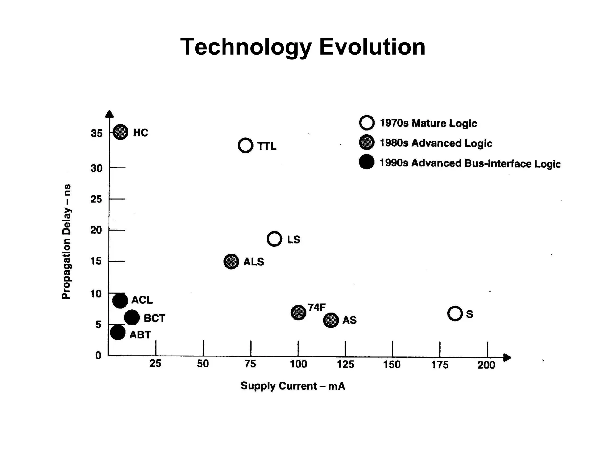
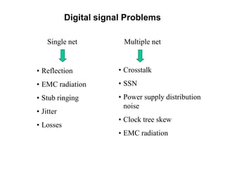
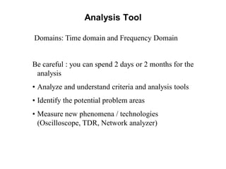
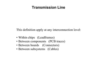
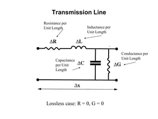
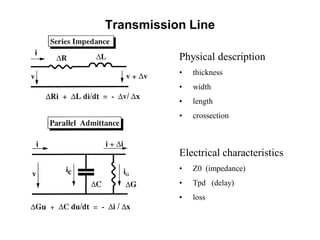
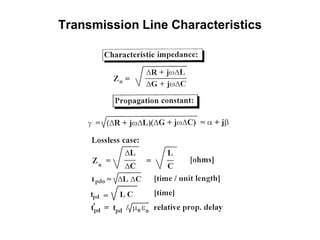
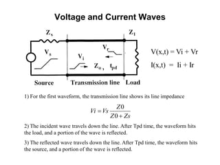
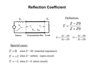
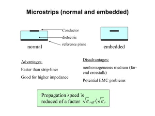
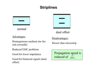

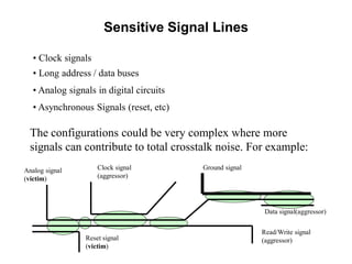
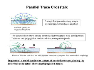
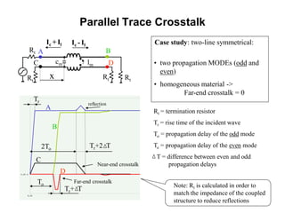
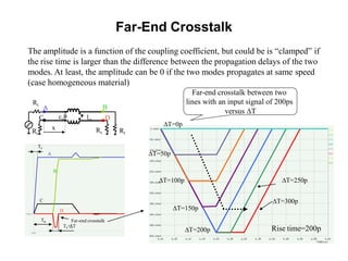
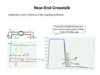
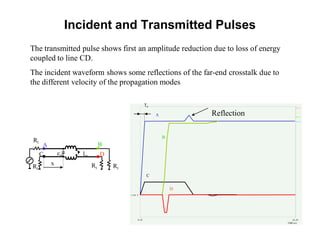
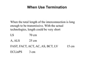

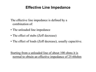
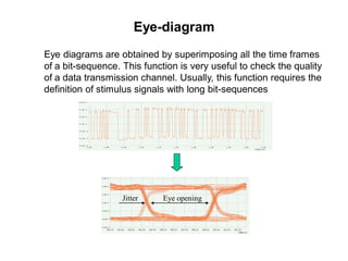
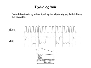
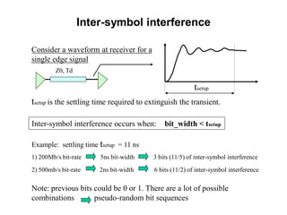
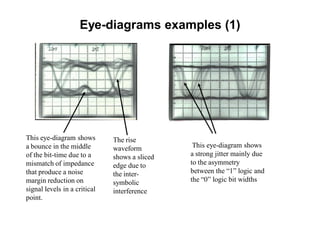
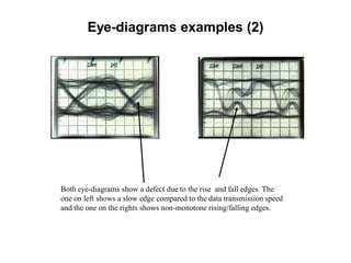
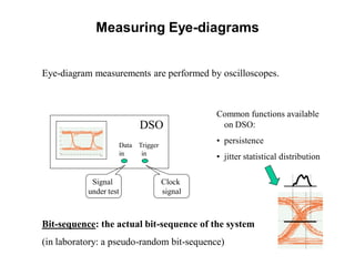
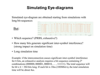
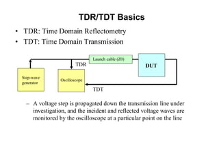
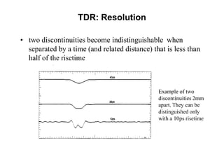
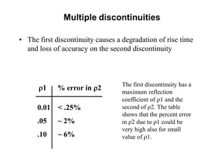
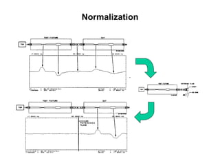
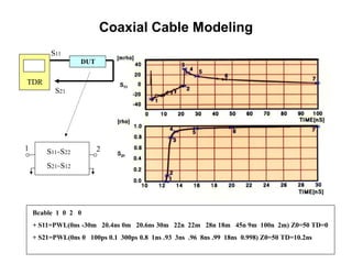
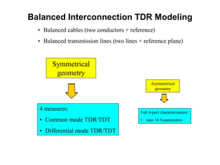
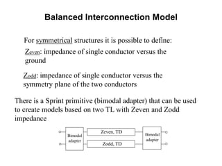
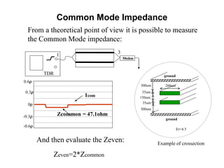
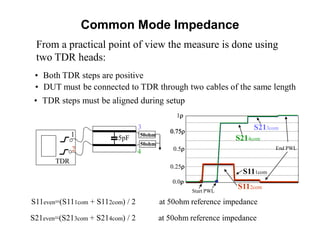
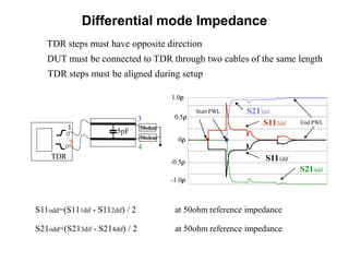
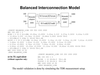
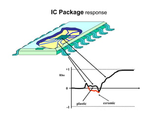
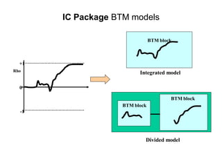
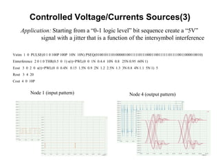
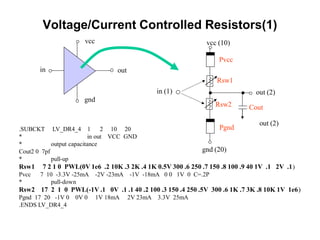
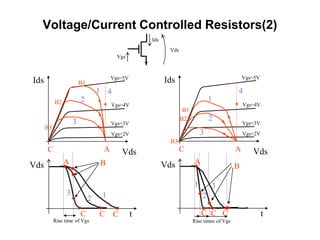
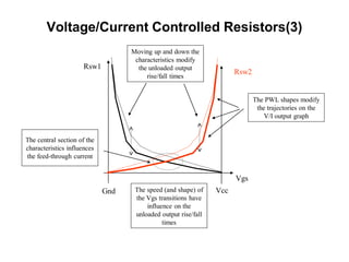

This document discusses signal integrity issues in digital systems. It covers topics like reflections, crosstalk, transmission line characteristics, eye diagrams and analysis tools. Reflections can cause problems like ringing at interconnect boundaries due to impedance mismatches. Crosstalk is unwanted coupling between signal lines and can reduce noise margins. Transmission lines are characterized by parameters like impedance and delay. Eye diagrams are used to analyze signal quality by superimposing waveforms. Analysis tools include oscilloscopes, TDR and simulating eye diagrams with long pseudorandom bit sequences. Maintaining signal integrity requires careful design of transmission line structures, termination, limiting crosstalk and avoiding interference between symbols.
![Signal Integrity - A Crash Course [R Lott]](https://cdn.slidesharecdn.com/ss_thumbnails/1cb0870c-cad3-4a68-ad41-8e9450fec5d8-170217191645-thumbnail.jpg?width=640&height=640&fit=bounds)