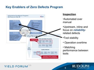
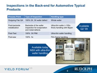
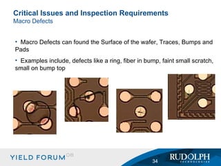
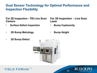
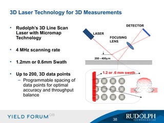
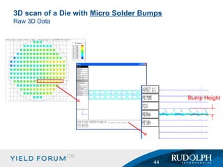
2008 Trends in the Back-end Rajiv Roy
Rudolph tools for back-end Use of inspection for automotive semiconductor Investment in 100% outgoing inspection –  Zero Defects PMI correlation –  Tool Correlation – Certification wafer Test floor Preventing probe card damage Inspection of CMOS sensors and TSV Micro bump / pillar bump   Through silicon stacking interconnect –  New Technology Flip-chip – advanced bumps –  Transition from conventional packaging Probe card analysis and test  - Darren James presentation Agenda
Rudolph - Where We Play – Tools for Back-End Inspection Metrology Analysis Global Support August - NSX RVSI  -  WS API - PrVX4
Use of Inspection for Automotive Semiconductor Investment in 100% Outgoing inspection – Zero Defects
Zero Defects and Automotive Semiconductor Industry Şafak Keçeci Infineon Regensburg June 12, 2007 Regensburg - Rudolph‘s European Yield Forum
Key Enablers of Zero Defects Program Inspection Automated over manual Upstream, inline and focus on  reliability -related defects Tool stability Operation overtime Matching performance between tools
Zero Defect as Key for Infineon Future  Customer Return Rate  Status April 2006 Products with 0 ppm:  Increase to … %
Inspections in the Back-end for Automotive Typical Products Available Q2 ‘09 Available today NSX with ultra-thin wafer handling Process Point Type of Inspection Handling type Outgoing Fab QA 100% 2X, 3X wafer defect Whole wafer Post-backside metallization Backside of the wafer inspection for evaporation and metal defects Ultra-thin wafer (~100u thick) handling with flipper Post-Test 100%  5X PMI Ultra-thin wafer handling  Post-saw 100%  5x  Film-frame handling
Use of Inspection for Automotive Semiconductor PMI (Probe Mark Inspection) Tool Correlation Certification wafer
T2T correlation and repeatability study was performed using PMI metrology data at customer site Tool Type: NSX115 with Basler Camera Wafer was chosen and eight bond pads were sampled for probe mark inspection. The product setup was created on RU02 and copied over to RU01 without detector training. The wafer was inspected 15 times on each tool.  Each time, PMI raw data report was generated and saved. The inspection was performed using 5X objective.  PMI  Tool-to-Tool Correlation at Customer Site DOE  Overview
Spec components tighter–camera, lenses, illumination Illumination matching, flat-fielding, Image distortion correction Re-do our system manufacturing build procedure Put a “golden tool” in class 10 clean-room Implement a “golden wafer” or a standard wafer design. Certify new standard wafers Certify all tools relative to “golden tool” What did Rudolph do to Enable Tool Matching? If your inspection tool supplier does not have Tools designed ground up for tool matching Standard Wafer  and the concept of  Golden Tool  in manufacturing Manufacturing methodologies – stringent key component quality along with tool certification procedures You do not have an inspection tool for automotive applications
Sample Plan Bondpad 1 Bondpad 2 Bondpad 3 Bondpad 4 Bondpad 5 Bondpad 6 Bondpad 7 Bondpad 8
Left Edge Proximity ( µm ) Results
Average Left Edge Proximity ( µm ) Results Average correlation between two tools running the same wafer >96% for bond pad edge proximity
Probe Mark Area ( µm ²) Results
Average Probe Mark Area ( µm ²) Results Average correlation between two tools running the same wafer >93% for probe mark area
Automotive industry requires a metrology approach to inspection Tools have to be designed ground up for tool matching Must implement  Standard Wafer  and the concept of  Golden Tool  in manufacturing Implement manufacturing methodologies – stringent key component quality along with tool certification procedures Using a single recipe, defects with >90% correlation between tools is achievable PMI for Automotive Products Conclusions
Test Floor Avoiding Damage to Probe Cards Detecting Tall Particles
Laser Dark-field  on NSX was used to detect particles Customer Supplied Rudolph Technologies with 2 – 300mm for inspection, with the focus of the inspection being  Partial Die on the Edge of the Wafer Inspection performed before probing to detect particles that could damage probe cards Target Defect Size is 100µm and greater Inspection setup Inspection performed with 100% laser dark-field No bright-field illumination 1x Inspection used the die size of the wafer 5x Inspection performed as bare\blanket wafer Tall Particle Detection Applications Study
Laser Dark-field With Laser Dark-field, the laser light hits the surface at an oblique angle Only light scattered normal to the surface is captured in the optics, since the optics are normal to the surface Defects that are large and angular (Particles, Large and Deep Scratches) Reflect More Light Normal to the Surface  Inspection Setup and Explanation Optics Incident Laser Light Particle
Images at 10X, Brightfield used only for image capture Red in images is laser reflecting off  feature Particles detected using Laser Dark-field
Defect Height Estimates 1 2 3 4 5 6 7 Measure defect height with focus – focus on wafer surface and then focus on defect top. 15 defects were measured
Defect Height Estimates 8 9 10 11
Defect Height Estimates 12 13 14 15
The use of laser dark-field will adequately detect tall particles The throughput will be effected by an extra dark-field pass The 2D defect size correlates fairly well with the expected height of the particle Using blank wafer inspection techniques, the entire surface of the wafer can be inspected for tall particles including the streets and edges of the wafer where there is no pattern Conclusions
Inspection of CMOS Sensors & TSV
Inspect glue dimensions of bubbles after adhesion Glass is pressed onto the silicon and the bubble size indicates the gap If bubbles are too small, then glass is too high. If the bubbles are too big, then the glass has been pressed too low 2x or 5x inspection mag depending on precision needed Bonding Control of glass Inspect vias for insufficient and excess glue
5x inspection mag used to inspect bottom side of the wafer and pixel area in one pass through the glass Inspection of Bottom side of CMOS Sensor Inspect sensor array and bottom side of glass carrier in single pass Bump Pads Via
The NSX is used at 3 different stages of the CMOS sensor assembly Customer is performing 100% inspection Using multiple tools with tool matching (recipe sharing) All inspections at 5x Bumped CMOS Imager based on TSV Inspect bumps, RDL, voids and damage to RDL
Micro Bump Through Silicon Stacking Interconnect Flip-chip
Pillar Bumps come in various shapes and sizes Height can vary from 5um to over 100um and diameter can vary from 20um to more They can have solder cap or not Typical applications include microprocessor, memory, etc. Copper Pillar Bump With Solder Cap Without Solder Cap CU - Pillar Bumps
Typical height is 20-30um Typical Pitch is 50um Due to small size of the bump and tight pitch number of I/Os  have significantly increased on a die Interconnection of choice for most TSV packages Micro Solder Bumps
Critical Issues and Inspection Requirements  Bump Dimensions / Bump Defects Bump Height Coplanarity: Best Fit Plane Method  Coplanarity: Seating Plane Method  Diameter Bridge Bump Missing Bump
Critical Issues and Inspection Requirements Macro Defects Macro Defects can found the Surface of the wafer, Traces, Bumps and Pads Examples include, defects like a ring, fiber in bump, faint small scratch, small on bump top
Copper Pillar Bumps Large Bump height variation requires sensor technology to be able to handle bumps from 5um to over 100um Sensor technology should  allow production throughput while maintaining measurement precision Technology is still evolving and ultimate inspection system needs to provide flexibility for current and future requirements Micro Solder Bumps Small nature of the bump (25um avg. height) requires high resolution sensor as compared to the requirements for standard solder bumps Large number of bumps and tight Pitch require high resolution sensor and large memory for data processing Number of bumps could be over 10,000/dies and 9,000,000/wafer Both Bump types require combination 3D and 2D inspection Inspection Challenges
Rudolph’s Approach to Micro Bump Inspection and Metrology
For 2D Inspection - TDI Line Scan Camera Surface Defect Inspection 2D Bump Metrology 2D Bump Defect For 3D Inspection  - Line Scan Laser Bump Coplanarity Bump Height Dual Sensor Technology for Optimal Performance and Inspection Flexibility
Rudolph’s 3D Line Scan Laser with Micromap Technology 4 MHz scanning rate 1.2mm or 0.6mm Swath Up to 200, 3D data points Programmable spacing of data points for optimal accuracy and throughput balance 3D Laser Technology for 3D Measurements DETECTOR LASER FOCUSING LENS 200 - 400  m 1.2 or .6 mm swath
Sample Inspection Case Studies
3D Scan of Copper Pillar Bumps Raw 3D Data
3D Scan of Copper Pillar Bumps Raw 3D Data Cross section of some bumps on a die Dark is lower pixels of 3D scan, yellow are tallest  Damaged Bump Height Good Bump Height
Sample Wafer Height Variation Across the Wafer Avg. Dia.= 26.6um Min. Dia.= 21.6um Max. Dia.= 35um Sigma = 2.8um Avg. Height = 18.7um Min. Height = 10.6um Max. Height = 30.14um Sigma = 4.0um
Copper Pillar Bump  Repeatability Results   WS Mean (15 Runs at 5 runs/Day)  WS STDV (15 Runs at 5 runs/Day)  Bump Height Average / Die -  Min  24.42 0.0085 Bump Height Average / Die -  Max  27.92 0.0147 Bump Height  wafer - Min  23.00 0.0246 Bump Height  wafer - Max  33.91 0.0451 Wafer Height Mean 25.31 0.0088 Wafer Height Stddev 1.13 0.0021
3D scan of a Die with  Micro Solder Bumps Raw 3D Data Bump Height
Micro Solder Bump  Repeatability Results Measurement Avg. (um) Min. (um) (col., row) Max. (um) (Col, row) 3 Sigma (um) True X Position -3.63 -17.91 (2, 12) 13.4 (13, 12) 0.48 True Y Position 1.41 -0.45 (2, 12) 3.8 (12, 12) 0.62 True Radial Position 5.81 0.2 (3, 12) 17.96 (2, 12) 0.51 Height 13.37 10.12 (2, 12) 17.86 (13, 12) 0.53 Diameter 31.36 27.63 (8, 4) 34.27 (13, 12) 0.75
Sample Captured Macro Defects
Throughputs Case 1  Throughput with handling based on 25 wafers/slot with 2.5X lens (2.8um pixel).  Bump heights ~25um (different die-size and bump count) 100% 3D – 11.0  - 12.7 WPH 100% 3D/2D – 7.4  - 8.2 WPH   Case 2 Throughput with handling based on 25 wafers/slot with 2.5X lens (2.8um pixel).  Bump heights ~40um (different die-size and bump count 100% 3D 100% 3D  - 11.8 WPH Bump count / wafer range approx 500,000 to 3 million
Conclusion of Microbump Inspection and Metrology Copper Pillar bumps and Micro bumps require high precision sensor both for 3D and 2D measurements Combination 2D/3D system is ideal for improved CoO Laser is well capable of inspecting varying bump heights and providing needed precision at production worthy throughput
Conclusions and Observations of Trends Use of Inspection for Automotive Semiconductor is increasing – it is essential component of Zero Defect Program Inspection tools have to be designed ground up for Tool correlation including certification wafer program Test Floors want to prevent damage to expensive probe cards because of tall particles. Rudolph offers a fast 2D solution for screening Inspection of CMOS Sensors and TSV devices is already entering production. High throughput systems like NSX are being used currently Micro Bump / Pillar Bump is inspected at production speeds by leading edge semiconductor manufacturers with very high accuracy and repeatability Probe Card Analysis and Test insights will be provided in Darren James presentation
Thank you!

Trends in the Backend for Semiconductor Wafer Inspection

  • 1.
    2008 Trends inthe Back-end Rajiv Roy
  • 2.
    Rudolph tools forback-end Use of inspection for automotive semiconductor Investment in 100% outgoing inspection – Zero Defects PMI correlation – Tool Correlation – Certification wafer Test floor Preventing probe card damage Inspection of CMOS sensors and TSV Micro bump / pillar bump Through silicon stacking interconnect – New Technology Flip-chip – advanced bumps – Transition from conventional packaging Probe card analysis and test - Darren James presentation Agenda
  • 3.
    Rudolph - WhereWe Play – Tools for Back-End Inspection Metrology Analysis Global Support August - NSX RVSI - WS API - PrVX4
  • 4.
    Use of Inspectionfor Automotive Semiconductor Investment in 100% Outgoing inspection – Zero Defects
  • 5.
    Zero Defects andAutomotive Semiconductor Industry Şafak Keçeci Infineon Regensburg June 12, 2007 Regensburg - Rudolph‘s European Yield Forum
  • 6.
    Key Enablers ofZero Defects Program Inspection Automated over manual Upstream, inline and focus on reliability -related defects Tool stability Operation overtime Matching performance between tools
  • 7.
    Zero Defect asKey for Infineon Future Customer Return Rate Status April 2006 Products with 0 ppm: Increase to … %
  • 8.
    Inspections in theBack-end for Automotive Typical Products Available Q2 ‘09 Available today NSX with ultra-thin wafer handling Process Point Type of Inspection Handling type Outgoing Fab QA 100% 2X, 3X wafer defect Whole wafer Post-backside metallization Backside of the wafer inspection for evaporation and metal defects Ultra-thin wafer (~100u thick) handling with flipper Post-Test 100% 5X PMI Ultra-thin wafer handling Post-saw 100% 5x Film-frame handling
  • 9.
    Use of Inspectionfor Automotive Semiconductor PMI (Probe Mark Inspection) Tool Correlation Certification wafer
  • 10.
    T2T correlation andrepeatability study was performed using PMI metrology data at customer site Tool Type: NSX115 with Basler Camera Wafer was chosen and eight bond pads were sampled for probe mark inspection. The product setup was created on RU02 and copied over to RU01 without detector training. The wafer was inspected 15 times on each tool. Each time, PMI raw data report was generated and saved. The inspection was performed using 5X objective. PMI Tool-to-Tool Correlation at Customer Site DOE Overview
  • 11.
    Spec components tighter–camera,lenses, illumination Illumination matching, flat-fielding, Image distortion correction Re-do our system manufacturing build procedure Put a “golden tool” in class 10 clean-room Implement a “golden wafer” or a standard wafer design. Certify new standard wafers Certify all tools relative to “golden tool” What did Rudolph do to Enable Tool Matching? If your inspection tool supplier does not have Tools designed ground up for tool matching Standard Wafer and the concept of Golden Tool in manufacturing Manufacturing methodologies – stringent key component quality along with tool certification procedures You do not have an inspection tool for automotive applications
  • 12.
    Sample Plan Bondpad1 Bondpad 2 Bondpad 3 Bondpad 4 Bondpad 5 Bondpad 6 Bondpad 7 Bondpad 8
  • 13.
    Left Edge Proximity( µm ) Results
  • 14.
    Average Left EdgeProximity ( µm ) Results Average correlation between two tools running the same wafer >96% for bond pad edge proximity
  • 15.
    Probe Mark Area( µm ²) Results
  • 16.
    Average Probe MarkArea ( µm ²) Results Average correlation between two tools running the same wafer >93% for probe mark area
  • 17.
    Automotive industry requiresa metrology approach to inspection Tools have to be designed ground up for tool matching Must implement Standard Wafer and the concept of Golden Tool in manufacturing Implement manufacturing methodologies – stringent key component quality along with tool certification procedures Using a single recipe, defects with >90% correlation between tools is achievable PMI for Automotive Products Conclusions
  • 18.
    Test Floor AvoidingDamage to Probe Cards Detecting Tall Particles
  • 19.
    Laser Dark-field on NSX was used to detect particles Customer Supplied Rudolph Technologies with 2 – 300mm for inspection, with the focus of the inspection being Partial Die on the Edge of the Wafer Inspection performed before probing to detect particles that could damage probe cards Target Defect Size is 100µm and greater Inspection setup Inspection performed with 100% laser dark-field No bright-field illumination 1x Inspection used the die size of the wafer 5x Inspection performed as bare\blanket wafer Tall Particle Detection Applications Study
  • 20.
    Laser Dark-field WithLaser Dark-field, the laser light hits the surface at an oblique angle Only light scattered normal to the surface is captured in the optics, since the optics are normal to the surface Defects that are large and angular (Particles, Large and Deep Scratches) Reflect More Light Normal to the Surface Inspection Setup and Explanation Optics Incident Laser Light Particle
  • 21.
    Images at 10X,Brightfield used only for image capture Red in images is laser reflecting off feature Particles detected using Laser Dark-field
  • 22.
    Defect Height Estimates1 2 3 4 5 6 7 Measure defect height with focus – focus on wafer surface and then focus on defect top. 15 defects were measured
  • 23.
  • 24.
  • 25.
    The use oflaser dark-field will adequately detect tall particles The throughput will be effected by an extra dark-field pass The 2D defect size correlates fairly well with the expected height of the particle Using blank wafer inspection techniques, the entire surface of the wafer can be inspected for tall particles including the streets and edges of the wafer where there is no pattern Conclusions
  • 26.
    Inspection of CMOSSensors & TSV
  • 27.
    Inspect glue dimensionsof bubbles after adhesion Glass is pressed onto the silicon and the bubble size indicates the gap If bubbles are too small, then glass is too high. If the bubbles are too big, then the glass has been pressed too low 2x or 5x inspection mag depending on precision needed Bonding Control of glass Inspect vias for insufficient and excess glue
  • 28.
    5x inspection magused to inspect bottom side of the wafer and pixel area in one pass through the glass Inspection of Bottom side of CMOS Sensor Inspect sensor array and bottom side of glass carrier in single pass Bump Pads Via
  • 29.
    The NSX isused at 3 different stages of the CMOS sensor assembly Customer is performing 100% inspection Using multiple tools with tool matching (recipe sharing) All inspections at 5x Bumped CMOS Imager based on TSV Inspect bumps, RDL, voids and damage to RDL
  • 30.
    Micro Bump ThroughSilicon Stacking Interconnect Flip-chip
  • 31.
    Pillar Bumps comein various shapes and sizes Height can vary from 5um to over 100um and diameter can vary from 20um to more They can have solder cap or not Typical applications include microprocessor, memory, etc. Copper Pillar Bump With Solder Cap Without Solder Cap CU - Pillar Bumps
  • 32.
    Typical height is20-30um Typical Pitch is 50um Due to small size of the bump and tight pitch number of I/Os have significantly increased on a die Interconnection of choice for most TSV packages Micro Solder Bumps
  • 33.
    Critical Issues andInspection Requirements Bump Dimensions / Bump Defects Bump Height Coplanarity: Best Fit Plane Method Coplanarity: Seating Plane Method Diameter Bridge Bump Missing Bump
  • 34.
    Critical Issues andInspection Requirements Macro Defects Macro Defects can found the Surface of the wafer, Traces, Bumps and Pads Examples include, defects like a ring, fiber in bump, faint small scratch, small on bump top
  • 35.
    Copper Pillar BumpsLarge Bump height variation requires sensor technology to be able to handle bumps from 5um to over 100um Sensor technology should allow production throughput while maintaining measurement precision Technology is still evolving and ultimate inspection system needs to provide flexibility for current and future requirements Micro Solder Bumps Small nature of the bump (25um avg. height) requires high resolution sensor as compared to the requirements for standard solder bumps Large number of bumps and tight Pitch require high resolution sensor and large memory for data processing Number of bumps could be over 10,000/dies and 9,000,000/wafer Both Bump types require combination 3D and 2D inspection Inspection Challenges
  • 36.
    Rudolph’s Approach toMicro Bump Inspection and Metrology
  • 37.
    For 2D Inspection- TDI Line Scan Camera Surface Defect Inspection 2D Bump Metrology 2D Bump Defect For 3D Inspection - Line Scan Laser Bump Coplanarity Bump Height Dual Sensor Technology for Optimal Performance and Inspection Flexibility
  • 38.
    Rudolph’s 3D LineScan Laser with Micromap Technology 4 MHz scanning rate 1.2mm or 0.6mm Swath Up to 200, 3D data points Programmable spacing of data points for optimal accuracy and throughput balance 3D Laser Technology for 3D Measurements DETECTOR LASER FOCUSING LENS 200 - 400  m 1.2 or .6 mm swath
  • 39.
  • 40.
    3D Scan ofCopper Pillar Bumps Raw 3D Data
  • 41.
    3D Scan ofCopper Pillar Bumps Raw 3D Data Cross section of some bumps on a die Dark is lower pixels of 3D scan, yellow are tallest Damaged Bump Height Good Bump Height
  • 42.
    Sample Wafer HeightVariation Across the Wafer Avg. Dia.= 26.6um Min. Dia.= 21.6um Max. Dia.= 35um Sigma = 2.8um Avg. Height = 18.7um Min. Height = 10.6um Max. Height = 30.14um Sigma = 4.0um
  • 43.
    Copper Pillar Bump Repeatability Results   WS Mean (15 Runs at 5 runs/Day) WS STDV (15 Runs at 5 runs/Day) Bump Height Average / Die - Min 24.42 0.0085 Bump Height Average / Die - Max 27.92 0.0147 Bump Height wafer - Min 23.00 0.0246 Bump Height wafer - Max 33.91 0.0451 Wafer Height Mean 25.31 0.0088 Wafer Height Stddev 1.13 0.0021
  • 44.
    3D scan ofa Die with Micro Solder Bumps Raw 3D Data Bump Height
  • 45.
    Micro Solder Bump Repeatability Results Measurement Avg. (um) Min. (um) (col., row) Max. (um) (Col, row) 3 Sigma (um) True X Position -3.63 -17.91 (2, 12) 13.4 (13, 12) 0.48 True Y Position 1.41 -0.45 (2, 12) 3.8 (12, 12) 0.62 True Radial Position 5.81 0.2 (3, 12) 17.96 (2, 12) 0.51 Height 13.37 10.12 (2, 12) 17.86 (13, 12) 0.53 Diameter 31.36 27.63 (8, 4) 34.27 (13, 12) 0.75
  • 46.
  • 47.
    Throughputs Case 1 Throughput with handling based on 25 wafers/slot with 2.5X lens (2.8um pixel).  Bump heights ~25um (different die-size and bump count) 100% 3D – 11.0 - 12.7 WPH 100% 3D/2D – 7.4 - 8.2 WPH   Case 2 Throughput with handling based on 25 wafers/slot with 2.5X lens (2.8um pixel).  Bump heights ~40um (different die-size and bump count 100% 3D 100% 3D - 11.8 WPH Bump count / wafer range approx 500,000 to 3 million
  • 48.
    Conclusion of MicrobumpInspection and Metrology Copper Pillar bumps and Micro bumps require high precision sensor both for 3D and 2D measurements Combination 2D/3D system is ideal for improved CoO Laser is well capable of inspecting varying bump heights and providing needed precision at production worthy throughput
  • 49.
    Conclusions and Observationsof Trends Use of Inspection for Automotive Semiconductor is increasing – it is essential component of Zero Defect Program Inspection tools have to be designed ground up for Tool correlation including certification wafer program Test Floors want to prevent damage to expensive probe cards because of tall particles. Rudolph offers a fast 2D solution for screening Inspection of CMOS Sensors and TSV devices is already entering production. High throughput systems like NSX are being used currently Micro Bump / Pillar Bump is inspected at production speeds by leading edge semiconductor manufacturers with very high accuracy and repeatability Probe Card Analysis and Test insights will be provided in Darren James presentation
  • 50.