Downloaded 210 times


The document discusses various techniques for electrically isolating devices in integrated circuits. It describes junction isolation, which uses reverse biased PN junctions, but this did not scale well as devices became smaller. Dielectric isolation techniques like LOCOS and STI were developed using deposited or thermally grown oxides. LOCOS had limitations like bird's beak encroachment affecting small device areas. STI involves etching trenches and depositing oxide to fill them, avoiding issues with LOCOS at small scales.
Introduction to device isolation, its importance in micro-fabrication, and understanding various techniques.
Key reasons for device isolation: preventing undesired paths, avoiding inversion layers, and reducing leakage currents.
Introduction to various device isolation techniques: Junction, Dielectric, LOCOS, and STI.
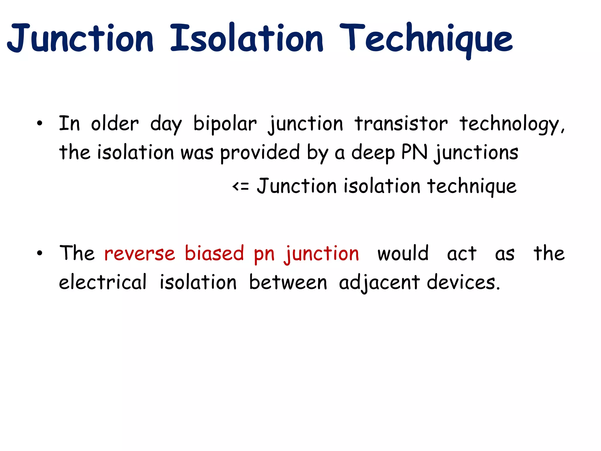
Description of Junction Isolation technique using PN junctions for electrical isolation and its limitations.
Discussion on Dielectric Isolation Technique and its common use of silicon dioxide.
Process of Etched Field oxide Isolation involving active areas surrounded by thick oxide barriers.
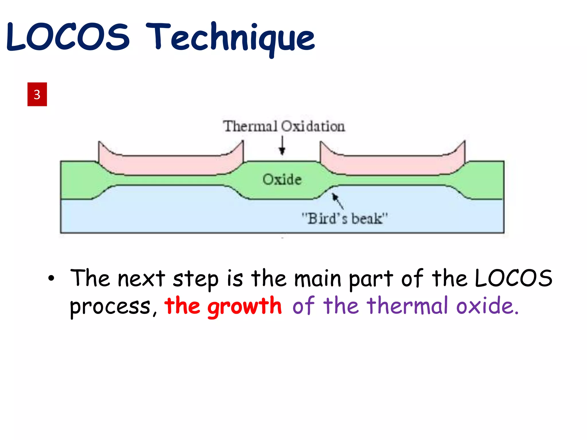
Overview of LOCOS technique, a local oxidation process, detailing its components for effectively preventing oxidation.
Techniques for photolithography and growing thermal oxide during the LOCOS process.
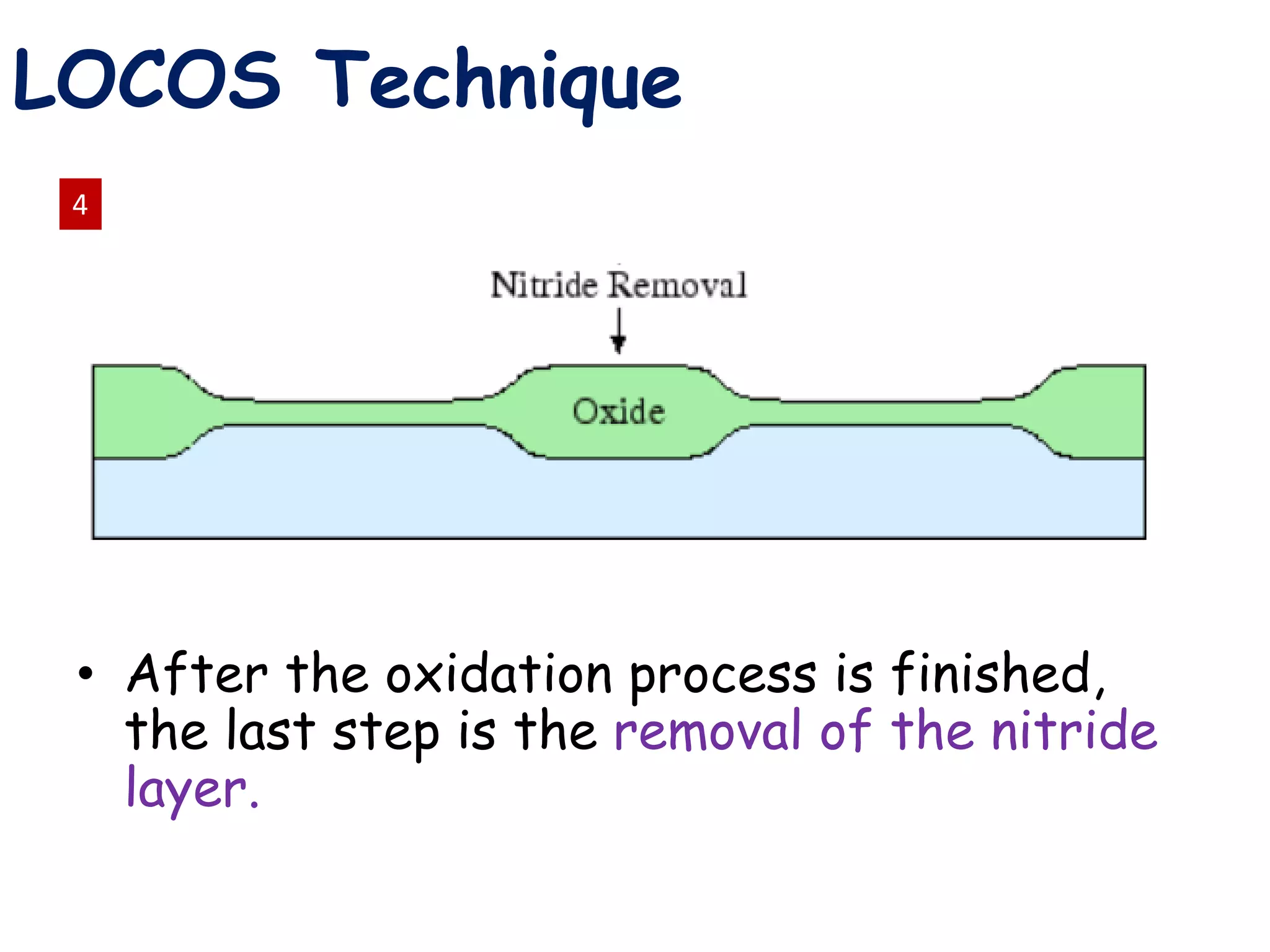
Final steps in LOCOS including removal of nitride and advantages like high oxide quality.
Limitations of LOCOS including the Bird’s Beak Problem, a challenge with shrinking device dimensions.
Introduction to Trench Isolation Technique involving cutting a trench in semiconductor for isolation.
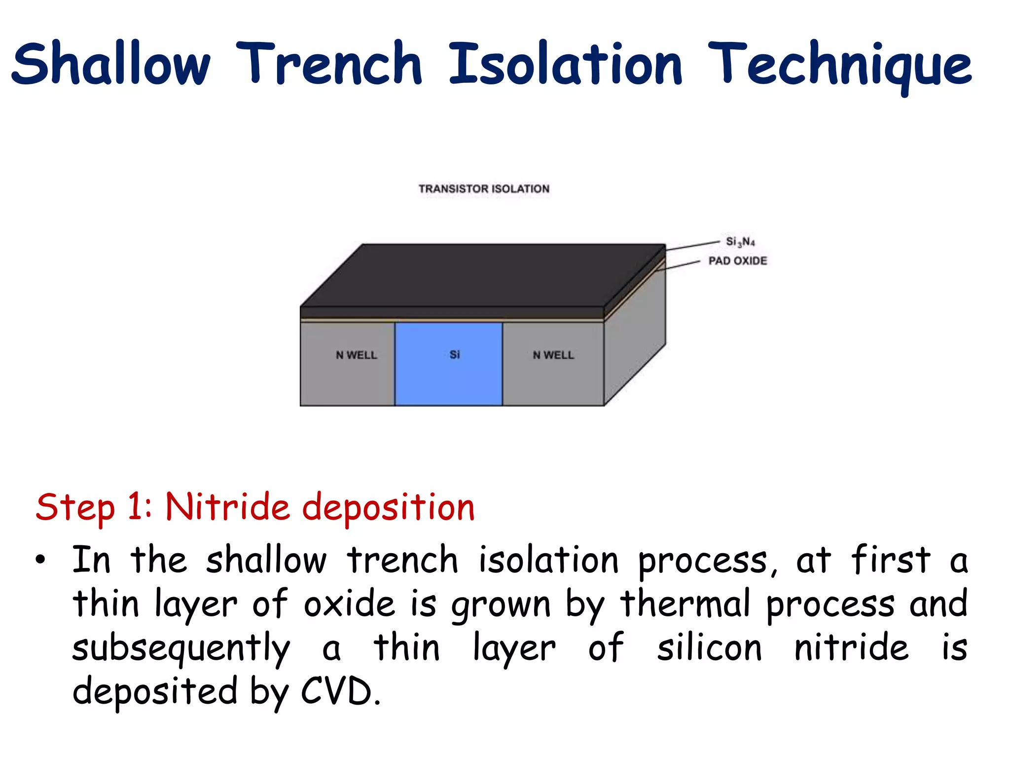
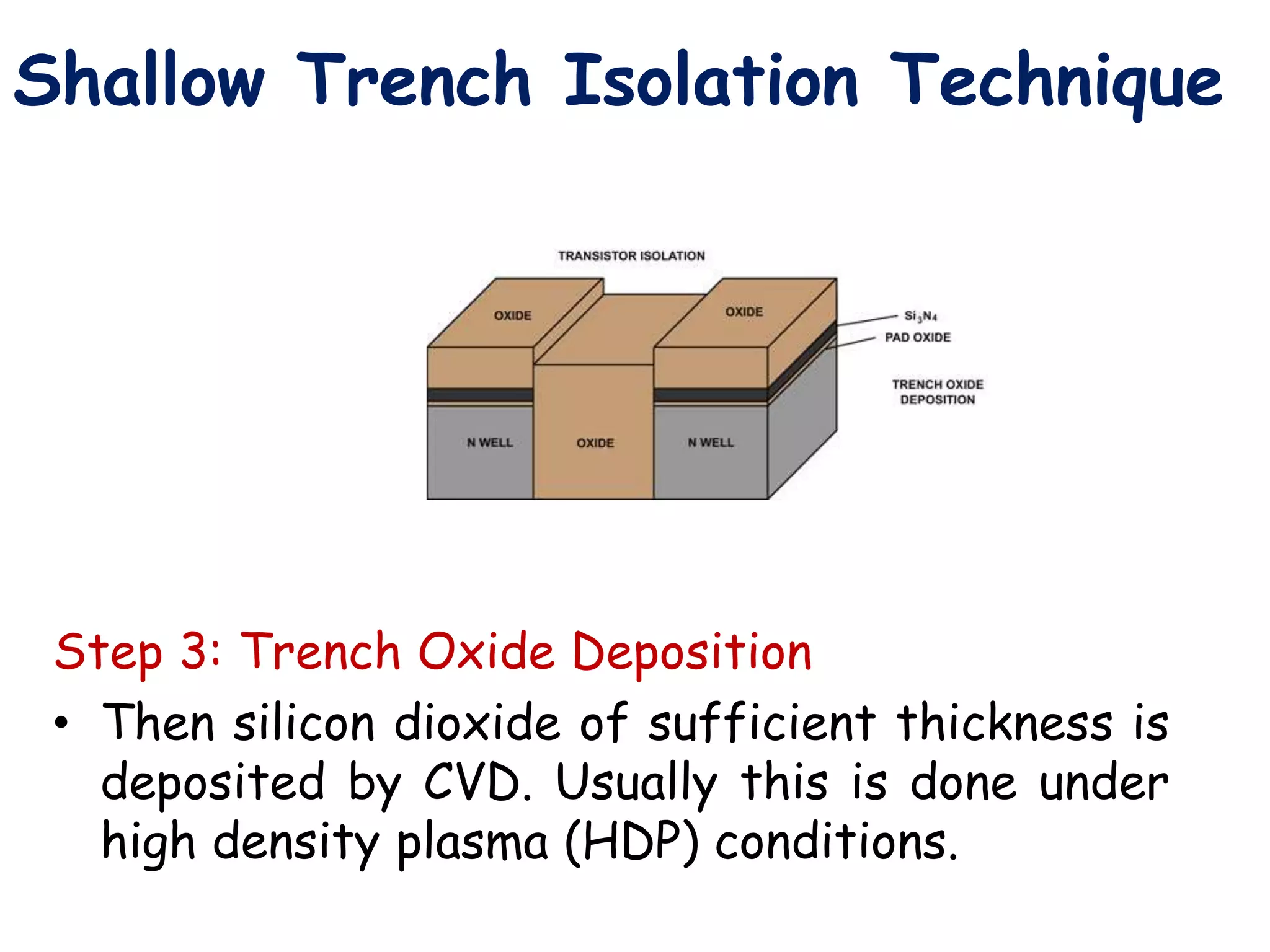
Steps in Shallow Trench Isolation including deposition of nitride, trench creation, and oxide deposition.
Final steps in Shallow Trench Isolation process including chemical mechanical planarization and nitride removal.
Final remarks on the Shallow Trench Isolation Technique.