MICROWIND AND LABVIEW
Introduction to MICROWIND
• MICROWIND is a basically a Digital Schematic Circuit Designing
software.
• MICROWIND is a simulation software which allows the designers to
simulate and design IC at Layout level
• MICROWIND is the most popular software for VLSI Circuit
designers
UNIT 1: INTRODUCTION AND FEATURES OF MICROWIND
• Nanometer Era
• Technology Scaling
• Microwind design Flow
• Microwind tool segments
DSCH , nanolambda ,Virtual fab , PROthumb (Transient Analysis of
Voltage and current,Transfer curve, Eye diagram, Parametric analysis, simulation on layout ) ,
PROtutor , MEMsim
• SOI
• Design Trends
• Technology rule files
Nanometer era
• nm stands for nanometer it is a unit of measure for length.
• 1nm is equal to 0.000000001 meters
• There are billions of transistors in a CPU that perform calculations through electrical signals by
switching on and off.
• In a CPU, nm is used to measure the size of the transistors that make up a processor
• In technological terms, a processor's nm is also referred to as a process node or technology process,
or just node.
• Manufacturing node represents density of transistors that can be printed on a chip
• Electronic chips are made in what is called a foundry.
• Some of the most important foundries(chip maker companies) are TSMC, Intel, Global Foundries or
Samsung
Nanometer size transistor advantages
• 1) Increased density of transistors in a IC
• 2) Improved energy efficient
• 3) Low power consumption
• 4) Reduction of size
• 5) Speed
• Moore's Law refers to Moore's perception that the number of
transistors on a microchip doubles every two years
• In 1965, Gordon E. Moore— The co-founder of Fairchild
Semiconductor and Intel.
• The principle that the speed and capability of computers can be
expected to double every two years, as a result of increases in the
number of transistors a microchip can contain.
• Advancements in digital electronics, such as the reduction in quality-
adjusted microprocessor prices, the increase in memory capacity
(RAM and flash), the improvement of sensors, and even the number
and size of pixels in digital cameras, are strongly linked to Moore's
law.
Technology Scaling:
• The reduction of the size, i.e., the dimensions of MOSFETs, is
commonly referred to as scaling.
• In order to meet the demand of high density chips in MOS
technology, it is required that MOSFET are scaled down i.e. reduction
in the size of transistor, so that high packaging density can be
achieved.
Technology Scaling Conti….
• In order to build high performance CMOS circuits certain design rules
need to be consider.
• As the device dimensions are reduced ,these design rules will change.
• Hence as the device dimensions are changing the electrical
parameters of the device are also need to be changed(scaled)
according to the current technology.
• There is a need to adjust fabrication process.
Advantages of Scaling:
• Improved current driving capability improves the device characteristics.
• Energy efficiency will be improved.
• Enhanced performance in terms of speed and power consumption.
• Reduction in size of the device.
• Cost of a chip decreases by twice.
• Increased density of transistors
Disadvantages of Scaling:
• The power consumption per unit area increases as devices are scaled
down. That means scaled devices run increasingly hot. This is a severe
performance limitation for scaled devices.
• Since scaling reduces the carrier mobility, gain of the device reduces.
• As the packing density per chip increases, due to higher power
density, the device becomes very hot and needs forced cooling at the
additional cost.
•MICROWIND Design flow
Microwind Design Flow:
• Microwind supports entire front-end to back-end
design flow.
• User can design digital circuits and compile here
using Verilog file.
• Microwind automatically generates a error free
CMOS layout.
• The CMOS layouts can be verified using inbuilt
mix-signal simulator and analysed for
DRC,crosstalks,delays,2D cross section,3D view
etc…
• DSCH program is a logic editor and simulator.
• DSCH can convert digital circuits into Verilog
file which can be further synthesized for FPGA
devices.
• The same Verilog file can be compiled for layout
conversion in microwind.
• For front-end designing , we have DSCH(digital
schematic editor) which posses in-built pattern
based simulator for digital circuits.
Microwind tool segments:
DSCH - Schematic Editor and Simulator
Nano Lambda - Precision CMOS Layout tool up to 22 nanometers
VirtualFab - Touch the Deep-Sub Micron Technology
PROthumb - Mixed Signal Simulation and Analysis
PROtutor - MOS characteristic viewer and trainer
MEMsim - Non Volatile Floating Gate Memory Simulators
DSCH (Digital Schematic Editor)
• DSCH is basically a digital schematic circuit designing software.
• This is a simulation software which allows the users to simulate and design integrated
circuit at physical description level.
• This is user friendly circuit simulation software and it is supported by huge symbol libraries
• The DSCH program is a logic editor and simulator.
• DSCH is used to validate the architecture of the logic circuit before the microelectronics
design is started.
• DSCH provides a user friendly environment for hierarchical logic design, and fast simulation
with delay analysis which allows the design and validation of complex logic structures.
• Designers can create logic circuits for interfacing with these controllers and verify software
programs using DSCH.
Logic circuit implementation of AND Gate
using DSCH
Nano Lambda (Precision CMOS Layout tool up to 22
nanometers)
• MICROWIND possess a precision CMOS layout editor called Nano Lmbda, which
supports technologies right from 1.2µm till 22nm nsFET Technology .
• This layout editor supports various technology transistors like MOSFET, FinFET and
nsFET .
• It has Design-error-free cell library.
• Sub-micron, deep-submicron, ultra deep-submicron, nanoscale technology support.
• It has Virtual components library (R,L,C, etc) for faster simulation response.
• Incredible translator from logic expression into compact design-error free layout.
• Powerful automatic compiler from Verilog structure circuit into layout.
• Extraction of all MOS width and length
Nano Lambda editor
Virtuso fab(Touch the deep-sub micron technology)
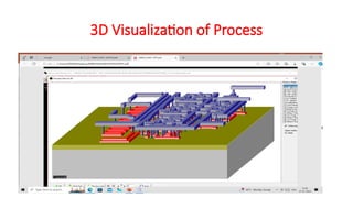
• Virtuso fab allows you to analyse and view cross sectional view of silicon
layers and 3D view of circuits.
• Virtuso fab contains 3D Fabrication process simulator with cross sectional
viewer.
• It allows a step by step 3D visualization of fabrication for any portion of
layout.
• We can see how contacts and mentalizations are created.
• We can check the planes of VDD ,VSS and other signals
• User can check oxide structure , and MOS lateral drain diffusion structure.
• It has 2D cross sectional viewer with strain technology support
3D Visualization of Process
PROthumb(Mixed Signal Simulation and
Analysis)
• In PROthumb time domain voltage and current waveforms are
available.
PROthumb(Mixed Signal Simulation and
Analysis)
• PROthumb has features like fast time domain, voltage and current estimations
• PROthumb has features like frequency estimation, delay estimation (No external
SPICE/Analog Simulator is required)
• Note: SPICE: Simulation Program with Integrated Circuit Emphasis
• SPICE is a simulation software
• It supports MOS Level 1, Level 3 and BSIM-4 Models for all technologies from 1.2 µm
to 14 nm.
• Note: MOS Level 1, Level 3 are first generation MOSFET Transistor technologies and
BSIM is Berkely Short-Channel IGFET Model
• IGFET: Insulated Gate FET
• Note: µm: Micrometre nm: Nanometer
PROthumb(Mixed Signal Simulation and
Analysis)
• It has forward and backward buttons to move in simulation results.
• It has huge device simulation model library.
• It supports Sophisticated parametric simulation to investigate the
effect of several key parameters on the circuit performances : R,L,C,
temperature, supply voltage, etc.
• It has Powerful Fast-Fourier Transform to support radio-frequency
circuit simulation.
• It displays DC/AC characteristics, signal frequency vs. time.
• It consists of Eye diagram view for signal output
PROtutor (MOS Characteristic Viwer & Trainer)
• PROtutor is a valuable screen to understand the MOS Characteristics
with a user interface.
• We can Change the model parameters (like channel length, Channel
width, Gate material, thickness and oxide layer) and we can see their
effects on Id/Vd , Id/Vg, threshold voltage vs Channel Length.
• Note: Id :drain current Vd : drain voltage Vg : Gate voltage
• You can also fit the simulations with measurements we made in test-
chips fabricated in 0.35, 0.25 and 0.18 µm
• Supports level1, level3 and BSIM4 MOS models.
MEMSIM : (Non volatile floating gate memory simulators)
• The double Gate MOS has been introduced in MICROWIND for the
simulation of non volatile memories like EPROM,EEPROM and FLASH.
• Note: EPROM : Erasable Programmable Read Only Memory
• EEPROM : Electrically Erasable Programmable Read Only Memory
• The programming is performed by a very high voltage supply on the
gate (7V in 0.12µm )
SOI(Silicon on insulator): • Silicon on insulator Technology refers to the use of layered
silicon-insulator-silicon substrate in place of conventional
silicon substrate in semiconductor manufacturing. As the
name suggests it is a process where the transistors are
fabricated on an insulators.
• Figure shows the Conventional bulk substrate for an NMOS
transistor and Partially depleted silicon-on-insulator for an
NMOS transistor.
• The fundamental difference between SOI and conventional
bulk CMOS technology is that the transistor source, drain, and
body are surrounded by insulating oxide rather than the
conductive substrate or well (called the bulk).
• Using an insulator eliminates most of the parasitic
capacitance of the diffusion regions. However, it means that
the body is no longer tied to GND or VDD through the
substrate or well.
• SOI offers numerous opportunities and challenges in the
design of low voltage and low-power CMOS circuits for both
analog and digital applications.
* In FD SOI, the body is thinner than the channel depletion width, so the body
charge is fixed and thus the body voltage does not change
* FD SOI has been difficult to manufacture because of the thin body
* No Floating body present
* In PD SOI, the body is thicker and its voltage can vary depending on how much
charge is present
* PD SOI is easier to manufacture, so appears to be the most promising
technology
* Floating body present
Transient analysis of voltage and currents
• Electric circuits will be subjected to sudden changes which may be in
the form of opening and closing of switches or sudden changes in
sources etc.
• Whenever such a change occurs, the circuit which was in a particular
steady state condition will go to another steady state condition.
• Transient analysis is the analysis of the circuits during the time it
changes from one steady state condition to another steady state
condition.
• Transient analysis will reveal how the currents and voltages are
changing during the transient period.
Transient analysis of voltage and currents
 When the circuit is driven with a constant direct current or DC
voltage, the approach to the steady-state over time can be examined.
 When the changes in magnitude of DC voltage/current source then
how the circuit current and voltage changes can also be determined
 How the phase and magnitude of the current and voltage are
different from those of the driver in alternating current or AC circuit is
also determined.
 In the time domain how the circuit responds to different arbitrary
driving waveforms can be also determined
Parametric Analysis
• The parametric analysis within Microwind is a powerful tool for rapid investigation
of the effect of some parameter variation on the behavior of the circuit.
• An example of analysis may be the effect of the load capacitance on the delay of a
gate
• Click on Analysis -> Parametric Analysis
• Select the desired output node on which the delay measurement or frequency
measurement is performed
• Then Click on a cell output node in the layout.
• The parametric analysis window appears.
• In the parameter menu, choose the item "node capacitance". Give the appropriate
range of analysis
Technology Rule File
• The technology file contains process specific parameters such as layer
thicknesses and the sheet resistance of the various layers.
• There are two sample technology files included for reference. These
technology files describe a generic CMOS and BiCMOS process.
• The first sub section begins with the < chip > satement
• The first two lines in the chip defines the chip dimensions in X and Y
directions
Output characteristics of MOSfet
MICRO WAVE LAB AND VIEW UNIT 1 RECENT.pptx

MICRO WAVE LAB AND VIEW UNIT 1 RECENT.pptx

  • 1.
  • 2.
    Introduction to MICROWIND •MICROWIND is a basically a Digital Schematic Circuit Designing software. • MICROWIND is a simulation software which allows the designers to simulate and design IC at Layout level • MICROWIND is the most popular software for VLSI Circuit designers
  • 3.
    UNIT 1: INTRODUCTIONAND FEATURES OF MICROWIND • Nanometer Era • Technology Scaling • Microwind design Flow • Microwind tool segments DSCH , nanolambda ,Virtual fab , PROthumb (Transient Analysis of Voltage and current,Transfer curve, Eye diagram, Parametric analysis, simulation on layout ) , PROtutor , MEMsim • SOI • Design Trends • Technology rule files
  • 4.
    Nanometer era • nmstands for nanometer it is a unit of measure for length. • 1nm is equal to 0.000000001 meters • There are billions of transistors in a CPU that perform calculations through electrical signals by switching on and off. • In a CPU, nm is used to measure the size of the transistors that make up a processor • In technological terms, a processor's nm is also referred to as a process node or technology process, or just node. • Manufacturing node represents density of transistors that can be printed on a chip • Electronic chips are made in what is called a foundry. • Some of the most important foundries(chip maker companies) are TSMC, Intel, Global Foundries or Samsung
  • 5.
    Nanometer size transistoradvantages • 1) Increased density of transistors in a IC • 2) Improved energy efficient • 3) Low power consumption • 4) Reduction of size • 5) Speed
  • 6.
    • Moore's Lawrefers to Moore's perception that the number of transistors on a microchip doubles every two years • In 1965, Gordon E. Moore— The co-founder of Fairchild Semiconductor and Intel. • The principle that the speed and capability of computers can be expected to double every two years, as a result of increases in the number of transistors a microchip can contain. • Advancements in digital electronics, such as the reduction in quality- adjusted microprocessor prices, the increase in memory capacity (RAM and flash), the improvement of sensors, and even the number and size of pixels in digital cameras, are strongly linked to Moore's law.
  • 7.
    Technology Scaling: • Thereduction of the size, i.e., the dimensions of MOSFETs, is commonly referred to as scaling. • In order to meet the demand of high density chips in MOS technology, it is required that MOSFET are scaled down i.e. reduction in the size of transistor, so that high packaging density can be achieved.
  • 8.
    Technology Scaling Conti…. •In order to build high performance CMOS circuits certain design rules need to be consider. • As the device dimensions are reduced ,these design rules will change. • Hence as the device dimensions are changing the electrical parameters of the device are also need to be changed(scaled) according to the current technology. • There is a need to adjust fabrication process.
  • 9.
    Advantages of Scaling: •Improved current driving capability improves the device characteristics. • Energy efficiency will be improved. • Enhanced performance in terms of speed and power consumption. • Reduction in size of the device. • Cost of a chip decreases by twice. • Increased density of transistors
  • 10.
    Disadvantages of Scaling: •The power consumption per unit area increases as devices are scaled down. That means scaled devices run increasingly hot. This is a severe performance limitation for scaled devices. • Since scaling reduces the carrier mobility, gain of the device reduces. • As the packing density per chip increases, due to higher power density, the device becomes very hot and needs forced cooling at the additional cost.
  • 11.
  • 12.
    Microwind Design Flow: •Microwind supports entire front-end to back-end design flow. • User can design digital circuits and compile here using Verilog file. • Microwind automatically generates a error free CMOS layout. • The CMOS layouts can be verified using inbuilt mix-signal simulator and analysed for DRC,crosstalks,delays,2D cross section,3D view etc… • DSCH program is a logic editor and simulator. • DSCH can convert digital circuits into Verilog file which can be further synthesized for FPGA devices. • The same Verilog file can be compiled for layout conversion in microwind. • For front-end designing , we have DSCH(digital schematic editor) which posses in-built pattern based simulator for digital circuits.
  • 13.
    Microwind tool segments: DSCH- Schematic Editor and Simulator Nano Lambda - Precision CMOS Layout tool up to 22 nanometers VirtualFab - Touch the Deep-Sub Micron Technology PROthumb - Mixed Signal Simulation and Analysis PROtutor - MOS characteristic viewer and trainer MEMsim - Non Volatile Floating Gate Memory Simulators
  • 14.
    DSCH (Digital SchematicEditor) • DSCH is basically a digital schematic circuit designing software. • This is a simulation software which allows the users to simulate and design integrated circuit at physical description level. • This is user friendly circuit simulation software and it is supported by huge symbol libraries • The DSCH program is a logic editor and simulator. • DSCH is used to validate the architecture of the logic circuit before the microelectronics design is started. • DSCH provides a user friendly environment for hierarchical logic design, and fast simulation with delay analysis which allows the design and validation of complex logic structures. • Designers can create logic circuits for interfacing with these controllers and verify software programs using DSCH.
  • 15.
    Logic circuit implementationof AND Gate using DSCH
  • 16.
    Nano Lambda (PrecisionCMOS Layout tool up to 22 nanometers) • MICROWIND possess a precision CMOS layout editor called Nano Lmbda, which supports technologies right from 1.2µm till 22nm nsFET Technology . • This layout editor supports various technology transistors like MOSFET, FinFET and nsFET . • It has Design-error-free cell library. • Sub-micron, deep-submicron, ultra deep-submicron, nanoscale technology support. • It has Virtual components library (R,L,C, etc) for faster simulation response. • Incredible translator from logic expression into compact design-error free layout. • Powerful automatic compiler from Verilog structure circuit into layout. • Extraction of all MOS width and length
  • 17.
  • 18.
    Virtuso fab(Touch thedeep-sub micron technology) • Virtuso fab allows you to analyse and view cross sectional view of silicon layers and 3D view of circuits. • Virtuso fab contains 3D Fabrication process simulator with cross sectional viewer. • It allows a step by step 3D visualization of fabrication for any portion of layout. • We can see how contacts and mentalizations are created. • We can check the planes of VDD ,VSS and other signals • User can check oxide structure , and MOS lateral drain diffusion structure. • It has 2D cross sectional viewer with strain technology support
  • 21.
  • 22.
    PROthumb(Mixed Signal Simulationand Analysis) • In PROthumb time domain voltage and current waveforms are available.
  • 23.
    PROthumb(Mixed Signal Simulationand Analysis) • PROthumb has features like fast time domain, voltage and current estimations • PROthumb has features like frequency estimation, delay estimation (No external SPICE/Analog Simulator is required) • Note: SPICE: Simulation Program with Integrated Circuit Emphasis • SPICE is a simulation software • It supports MOS Level 1, Level 3 and BSIM-4 Models for all technologies from 1.2 µm to 14 nm. • Note: MOS Level 1, Level 3 are first generation MOSFET Transistor technologies and BSIM is Berkely Short-Channel IGFET Model • IGFET: Insulated Gate FET • Note: µm: Micrometre nm: Nanometer
  • 24.
    PROthumb(Mixed Signal Simulationand Analysis) • It has forward and backward buttons to move in simulation results. • It has huge device simulation model library. • It supports Sophisticated parametric simulation to investigate the effect of several key parameters on the circuit performances : R,L,C, temperature, supply voltage, etc. • It has Powerful Fast-Fourier Transform to support radio-frequency circuit simulation. • It displays DC/AC characteristics, signal frequency vs. time. • It consists of Eye diagram view for signal output
  • 25.
    PROtutor (MOS CharacteristicViwer & Trainer) • PROtutor is a valuable screen to understand the MOS Characteristics with a user interface. • We can Change the model parameters (like channel length, Channel width, Gate material, thickness and oxide layer) and we can see their effects on Id/Vd , Id/Vg, threshold voltage vs Channel Length. • Note: Id :drain current Vd : drain voltage Vg : Gate voltage • You can also fit the simulations with measurements we made in test- chips fabricated in 0.35, 0.25 and 0.18 µm • Supports level1, level3 and BSIM4 MOS models.
  • 27.
    MEMSIM : (Nonvolatile floating gate memory simulators) • The double Gate MOS has been introduced in MICROWIND for the simulation of non volatile memories like EPROM,EEPROM and FLASH. • Note: EPROM : Erasable Programmable Read Only Memory • EEPROM : Electrically Erasable Programmable Read Only Memory • The programming is performed by a very high voltage supply on the gate (7V in 0.12µm )
  • 28.
    SOI(Silicon on insulator):• Silicon on insulator Technology refers to the use of layered silicon-insulator-silicon substrate in place of conventional silicon substrate in semiconductor manufacturing. As the name suggests it is a process where the transistors are fabricated on an insulators. • Figure shows the Conventional bulk substrate for an NMOS transistor and Partially depleted silicon-on-insulator for an NMOS transistor. • The fundamental difference between SOI and conventional bulk CMOS technology is that the transistor source, drain, and body are surrounded by insulating oxide rather than the conductive substrate or well (called the bulk). • Using an insulator eliminates most of the parasitic capacitance of the diffusion regions. However, it means that the body is no longer tied to GND or VDD through the substrate or well. • SOI offers numerous opportunities and challenges in the design of low voltage and low-power CMOS circuits for both analog and digital applications.
  • 29.
    * In FDSOI, the body is thinner than the channel depletion width, so the body charge is fixed and thus the body voltage does not change * FD SOI has been difficult to manufacture because of the thin body * No Floating body present * In PD SOI, the body is thicker and its voltage can vary depending on how much charge is present * PD SOI is easier to manufacture, so appears to be the most promising technology * Floating body present
  • 31.
    Transient analysis ofvoltage and currents • Electric circuits will be subjected to sudden changes which may be in the form of opening and closing of switches or sudden changes in sources etc. • Whenever such a change occurs, the circuit which was in a particular steady state condition will go to another steady state condition. • Transient analysis is the analysis of the circuits during the time it changes from one steady state condition to another steady state condition. • Transient analysis will reveal how the currents and voltages are changing during the transient period.
  • 33.
    Transient analysis ofvoltage and currents  When the circuit is driven with a constant direct current or DC voltage, the approach to the steady-state over time can be examined.  When the changes in magnitude of DC voltage/current source then how the circuit current and voltage changes can also be determined  How the phase and magnitude of the current and voltage are different from those of the driver in alternating current or AC circuit is also determined.  In the time domain how the circuit responds to different arbitrary driving waveforms can be also determined
  • 35.
    Parametric Analysis • Theparametric analysis within Microwind is a powerful tool for rapid investigation of the effect of some parameter variation on the behavior of the circuit. • An example of analysis may be the effect of the load capacitance on the delay of a gate • Click on Analysis -> Parametric Analysis • Select the desired output node on which the delay measurement or frequency measurement is performed • Then Click on a cell output node in the layout. • The parametric analysis window appears. • In the parameter menu, choose the item "node capacitance". Give the appropriate range of analysis
  • 36.
    Technology Rule File •The technology file contains process specific parameters such as layer thicknesses and the sheet resistance of the various layers. • There are two sample technology files included for reference. These technology files describe a generic CMOS and BiCMOS process. • The first sub section begins with the < chip > satement • The first two lines in the chip defines the chip dimensions in X and Y directions
  • 38.