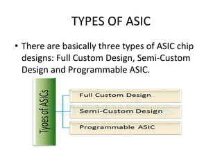
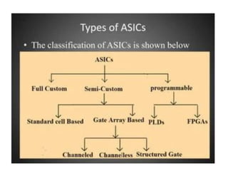
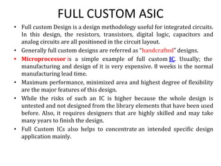
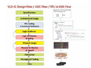
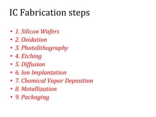
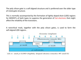
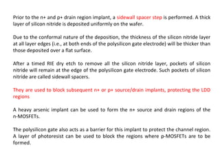
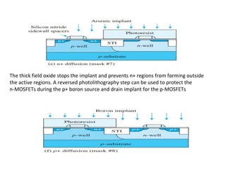
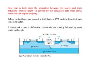
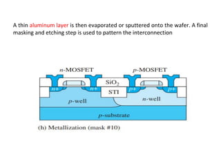
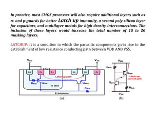
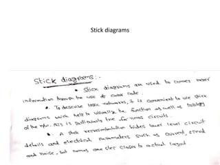
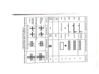
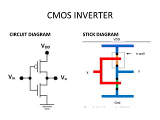
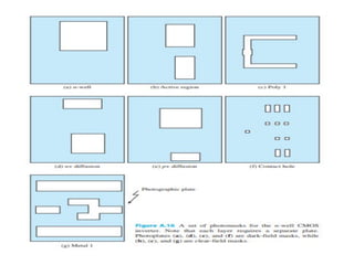
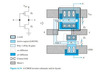
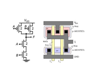
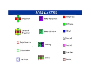
Unit-I
VLSI FABRICATION
TECHNOLOGY
CONTENTS
• Evolution of ICs Fabrication
• Introduction to ASIC’S
• ASIC’S Classification
• Typical ASIC/VLSI Design flow
• IC Fabrication steps
• Art of Miniaturization
• VLSI Processes
– Twin-well process
– MOSFET
– Resistors,
– Capacitors
– Pn junction diodes.
Cont.
• BICMOS process
• Lateral pnp transistor
• P-base and pinch based resistors
• Stick Diagrams
• VLSI Design rules
• VLSI LAYOUT
• Layouts for CMOS inverter ,CMOS nand and nor
gates
• Beyond 20nm Technology-FinFET
• The semiconductor industry has evolved from the first ICs of the early
1970s and matured rapidly since then.
• Early small-scale integration ( SSI ) ICs contained a few (1 to 10) logic
gates—NAND gates, NOR gates, and so on—amounting to a few tens of
transistors.
• The era of medium-scale integration ( MSI ) increased the range of
integrated logic available to counters and similar, larger scale, logic
functions.
• The era of large-scale integration ( LSI ) packed even larger logic functions,
such as the first microprocessors, into a single chip.
• The era of very large-scale integration ( VLSI ) now offers 64-bit
microprocessors, complete with cache memory and floating-point
arithmetic units—well over a million transistors—on a single piece of
silicon. As CMOS process technology improves, transistors continue to get
smaller and ICs hold more and more transistors.
• Some people (especially in Japan) use the term ultralarge scale integration
( ULSI).
Evolution of ICs Fabrication
• The earliest ICs used bipolar technology and the majority of logic ICs used either
transistor– transistor logic ( TTL ) or emitter-coupled logic (ECL).
• Although invented before the bipolar transistor, the metal-oxide-silicon ( MOS )
transistor was initially difficult to manufacture because of problems with the oxide
interface. As these problems were gradually solved, metal-gate n -channel MOS (
nMOS or NMOS ) technology developed in the 1970s.
• At that time MOS technology required fewer masking steps, was denser, and
consumed less power than equivalent bipolar ICs. This meant that, for a given
performance, an MOS IC was cheaper than a bipolar IC and led to investment and
growth of the MOS IC market.
• By the early 1980s the aluminum gates of the transistors were replaced by
polysilicon gates, but the name MOS remained.
• The introduction of polysilicon as a gate material was a major improvement in
CMOS technology, making it easier to make two types of transistors, n -channel
MOS and p -channel MOS transistors, on the same IC— a complementary MOS (
CMOS , never cMOS) technology.
• The principal advantage of CMOS over NMOS is lower power consumption.
Another advantage of a polysilicon gate was a simplification of the fabrication
process, allowing devices to be scaled down in size.
ASIC
• An ASIC (Application Specific Integrated Circuit)
or CSP (Customer Specific Product) is a custom IC
that is designed, planned, developed, and used for
a specific purpose, with the mission of being
optimized, efficient, and having all the required
functionalities and features to be used in a specific
application for a single customer.
.
• Some examples of popular ASIC chip include
•a chip with microprocessor for cellular
phones to work,
•a chip for a satellite,
•a chip for a talking toy bear, and
•a chip used for the voice recorder.
• Some ICs that are not ASICs
include memory chips like ROM, DRAM; ICs
at LSI, SSI and MSI levels etc.
.• Using an ASIC chip, the major advantage is that,
overall design can be made into one integrated
circuit and the number of additional circuits can
be reduced.
• Modern ASIC chip designs generally include 32-bit
processors, memory blocks and other large
building blocks.
• Such a modern ASIC chip is known as SoC
(System-on-a-Chip).
• Today, many digital ASIC designers use hardware
description languages (HDLs) like Verilog and
VHDL, to describe the function and design of ASIC
chip.
TYPES OF ASIC
• There are basically three types of ASIC chip
designs: Full Custom Design, Semi-Custom
Design and Programmable ASIC.
FULL CUSTOM ASIC
• Full custom Design is a design methodology useful for integrated circuits.
In this design, the resistors, transistors, digital logic, capacitors and
analog circuits are all positioned in the circuit layout.
• Generally full custom designs are referred as “handcrafted” designs.
• Microprocessor is a simple example of full custom IC. Usually; the
manufacturing and design of it is very expensive. 8 weeks is the normal
manufacturing lead time.
• Maximum performance, minimized area and highest degree of flexibility
are the major features of this design.
• While the risks of such an IC is higher because the whole design is
untested and not designed from the library elements that have been used
before. Also, it requires designers that are highly skilled and may take
many years to finish the design.
• Full Custom ICs also helps to concentrate an intended specific design
application mainly.
SEMICUSTOM DESIGN
• Semi-Custom design is an alternative to full-custom
designs.
• Here, we can use components from a standard library for
design purposes.
• Thus, in semicustom ASIC designs, all logic cells are
predesigned and some mask layers are only customized.
• The advantage of using predesigned logic cells from the
library is that, it can make semi-custom ASIC chip designs
easier. Standard cell libraries are usually designed using
full custom designs
.
• There are basically two types of semicustom
ASICs:
• Standard Cell Based ASIC and
• Gate Array Based ASIC.
Standard Cell Based ASICs
• A standard cell based ASIC commonly uses predesigned
logic cells like logic gates, flip flops, multiplexers,
demultiplexers etc. These predesigned logic cells are
known as Standard Cells.
• Flexible blocks also known as standard cell areas in the
ASIC design consist of many rows of standard cells.
• The standard cell areas can be usually used in combination
with larger standard cells like microcontrollers.
The larger standard cells are also known by the names
Megacells, Megafunctions, System Level Macros, Full
custom blocks, Fixed Blocks, cores or System Level Macros.
.
.
• Placement and providing Interconnection of
cells is the major role of the ASIC designer
here. Some advantages of using standard
cell based designs include save money,
reduced time and less risk compared to full
custom designs.
• The disadvantage is the time and expense to
make a standard library and to fabricate
these designs.
Gate Array Based ASICs
.• Gate Array Based ASIC chip is a prefabricated silicon chip in
which transistors, logic gates, and other active devices are
placed at predefined positions and manufactured on a wafer.
• Predefined pattern of gate array based ASIC is known
as Base Array. The element or logic cell present in the base
array is often called as Base Cell.
• Usually gate array based ASIC designs are known popularly
by the name Masked Gate Array.
• Here the ASIC designer can choose predesigned logic cells
from the gate array library for better and easy design.
.
• The cells present in the gate array library are often called
as Macros. Reduced time, low cost are some of its
advantages compared to standard cell and full custom
designs.
• Three types of Gate Array Based ASICs are:
❖ Channeled Gate Arrays,
❖ Channeless Gate Arrays and
❖ Structured Gate Array.
• In Channeled Gate Array, the space for interconnect between
the rows of cells are fixed in height. While in Channeless Gate
Array, there is no predefining space between the rows of
cells. Structured Gate Array or Embedded Gate
Array combines both the features of standard cell based and
gate array based ASICs
Programmable ASIC
• Programmable ASICs are classified into
• Programmable Logic Devices and
• Field Programmable Gate Arrays.
.
• PLDs are electronic devices used to build
reconfigurable circuits.
• Unique features of PLDs are fast turn around, large
programmable interconnect, no customized logic
cells and mask layers.
• PAL, PLA, GAL ROM, PROM, EPROM, EEPROM,
UVPROM etc. are some examples of programmable
ICs
.• FPGAs are complex and larger reconfigurable devices.
Unique features of Field Programmable Gate
Arrays include programming logic cells and interconnect
and here no mask layer is customized.
Programming of an FPGA
• The behavior of the FPGA is the user provides a
design in a Hardware Description Language (HDL)
or as a schematic design.
• The HDL form is more suited to work with large
structures because it's possible to specify
high-level functional behavior rather than drawing
every piece by hand.
• However, schematic entry can allow for easier
visualization of a design and its
component modules.
.
• Using an electronic design automation tool, a
technology-mapped netlist is generated. The netlist can
then be fit to the actual FPGA architecture using a process
called place-and-route, usually performed by the FPGA
company's proprietary place-and-route software.
• The user will validate the map, place and route results
via timing analysis, simulation and other verification and
validation methodologies.
• Once the design and validation process is complete, the
binary file generated, typically using the FPGA vendor's
proprietary software, is used to (re-)configure the FPGA.
• This file is transferred to the FPGA/CPLD via a serial
interface (JTAG) or to an external memory device like
an EEPROM.
.
• Design Entry: In the step, the logic design is created using a Hardware
Description Language (HDL) like VHDL or Verilog or with the help of
Schematic entry.
• Logic Synthesis: Once the logic is designed using HDL or Schematic
entry, the next step is to extract the description of the logic cells and
their interconnections. This information is also called as Netlist.
• System Partitioning: The next step is to logically divide the entire
system into small ASIC sized blocks.
• Pre-layout Simulation: Before going into the actual physical layout of
the design, a simulation tool checks the circuit for proper working. In
fact, this process is performed at every step so that if any errors are
found, then it would be easy to correct them at this stage itself. The
process until this step is usually regarded as Logical Design. The steps
after this are related to the actual physical layout of the design.
.
• Floorplanning: The first step in the physical design is arrange all the blocks of
the circuit on the chip.
• Placement: In this step, the location of the logic cells in a block are set.
• Routing: Once the placement of the blocks and cells is completed, then it is
time to create the connections between the cells and the blocks.
• Extraction: The next step is to determine the resistance and capacitance of the
interconnections previously made, since they decide the delay of the signal.
Also, the delays are calculated at this stage.
• Post-layout Simulation: Once the physical design is complete, the circuit is
again tested for working. The delays previously calculated are also taken into
consideration for the simulation process.
• Design Rule Check (DRC): Final step is to verify the layout of the entire circuit
and check whether it complies with the design rule specifications.
Figure 1.10 shows the sequence of steps to design an ASIC; we call this a design flow . The
steps are listed below (numbered to correspond to the labels in Figure 1.10) with a brief
description of the function of each step.
1. Design entry. Enter the design into an ASIC design system, either using a hardware
description language ( HDL ) orschematic entry .
2. Logic synthesis. Use an HDL (VHDL or Verilog) and a logic synthesis tool to produce a
netlist —a description of the logic cells and their connections.
3. System partitioning. Divide a large system into ASIC-sized pieces.
4. Prelayout simulation. Check to see if the design functions correctly.
5. Floorplanning. Arrange the blocks of the netlist on the chip.
6. Placement. Decide the locations of cells in a block.
7. Routing. Make the connections between cells and blocks.
8. Extraction. Determine the resistance and capacitance of the interconnect.
9. Postlayout simulation. Check to see the design still works with the added loads of the
interconnect.
Steps 1–4 are part of logical design , and steps 5–9 are part of physical design
Design Flow Steps
IC Fabrication steps
• 1. Silicon Wafers
• 2. Oxidation
• 3. Photolithography
• 4. Etching
• 5. Diffusion
• 6. Ion Implantation
• 7. Chemical Vapor Deposition
• 8. Metallization
• 9. Packaging
IC Fabrication Steps
The basic IC fabrication steps will be described in the following sections. Some of these
steps may be carried out many times, in different combinations and/or processing
conditions during a complete fabrication run.
1. Silicon Wafers
The starting material for modern integrated circuits is very-high-purity, single-crystal
silicon. The material is initially grown as a single crystal ingot. It takes the shape of a
steel-gray solid cylinder 10 cm to 30 cm in diameter and can be one to two meters in
length. This crystal is then sawed (like a loaf of bread) to produce circular wafers that are
400μm to 600μm thick (a micrometer, or micron, μm, is a millionth of a meter). The surface
of the wafer is then polished to a mirror finish using chemical and mechanical polishing
(CMP) techniques.
The basic electrical and mechanical properties of the wafer :
It depend on the orientation of the crystalline structure, the impurity concentrations, and the
type of impurities present. These variables are strictly controlled during crystal growth. A
specific amount of impurities can be added to the pure silicon in a process known as doping.
This allows the alteration of the electrical properties of the silicon, in particular its resistivity.
Depending on the types of impurity, either holes (in p-type silicon) or electrons (in n-type
silicon) can be responsible for electrical conduction. If a large number of impurity atoms is
added, the silicon will be heavily doped (e.g., concentration > ∼1018 atoms/cm−3 ). When
designating the relative doping concentrations in semiconductor material, it is common to
use the + and – symbols. A heavily doped (low-resistivity) n-type silicon wafer is referred to as
n+material, while a lightly doped material (e.g., concentration < ∼1016 atoms/cm−3 ) is
referred to as n−. Similarly, p+ and p− designations refer to the heavily doped and lightly
doped p-type regions, respectively.
1.2 Oxidation:
In oxidation, silicon reacts with oxygen to form silicon dioxide (SiO2). To speed up this
chemical reaction, it is necessary to carry out the oxidation at high temperatures (e.g.,
1000–1200°C) and inside ultraclean furnaces. To avoid the introduction of even small
quantities of contaminants (which could significantly alter the electrical properties of the
silicon), it is necessary to operate in a clean room . Particle filters are used to ensure that the
airflow in the processing area is free from dust. All personnel must protect the clean-room
environment by wearing special lint-free clothing that covers a person from head to toe.
The oxygen used in the reaction can be introduced either as a high-purity gas
(referred to as a “dry oxidation”) or as steam (forming a “wet oxidation”). In
general, wet oxidation has a faster growth rate, but dry oxidation gives better
electrical characteristics. The thermally grown oxide layer has excellent electrical
insulation properties. The dielectric strength for SiO2 is approximately 107 V/cm. It
has a dielectric constant of about 3.9, and it can be used to form excellent MOS
capacitors. Silicon dioxide can also serve as an effective mask against many
impurities, allowing the introduction of dopants into the silicon only in regions that
are not covered with oxide
Silicon dioxide is a transparent film, and the silicon surface is highly reflective. If white light
is shone on an oxidized wafer, constructive and destructive interference will cause certain
colors to be reflected. The wavelengths of the reflected light depend on the thickness of the
oxide layer. In fact, by categorizing the color of the wafer surface, one can deduce the
thickness of the oxide layer.
1.3 Photolithography
Mass production with economy of scale is the primary reason for the tremendous
impact VLSI has had on our society. The surface patterns of the various
integrated-circuit components can be defined repeatedly using photolithography.
The sequence of photolithographic steps is as illustrated in Fig. 1.
Contd..
The wafer surface is coated with a photosensitive layer called photoresist, using a spin-on
technique. After this, a photographic plate with drawn patterns (e.g., a quartz plate with
chromium layer for patterning) will be used to selectively expose the photoresist under a
deep ultraviolet illumination (UV). The exposed areas will become softened (for positive
photoresist). The exposed layer can then be removed using a chemical developer, causing
the mask pattern to be duplicated on the wafer. Very fine surface geometries can be
reproduced accurately by this technique. Furthermore, the patterns can be projected
directly onto the wafer, or by using a separate photomask produced by a 10x “step and
repeat” reduction technique as shown in Fig. 2
Contd..
The patterned photoresist layer can be used as an effective masking layer to protect
materials below from wet chemical etching or reactive ion etching (RIE). Silicon
dioxide, silicon nitride, polysilicon, and metal layers can be selectively removed
using the appropriate etching methods (see next section). After the etching step(s),
the photoresist is stripped away, leaving behind a permanent pattern of the
photomask on the wafer surface
1.4 Etching :
To permanently imprint the photographic patterns onto the wafer, chemical (wet)
etching or RIE dry etching procedures can be used. Chemical etching is usually referred
to as wet etching. Different chemical solutions can be used to remove different layers.
For example, hydrofluoric (HF) acid can be used to etch SiO2, potassium hydroxide
(KOH) for silicon, phosphoric acid for aluminum, and so on. In wet etching, the
chemical usually attacks the exposed regions that are not protected by the photoresist
layer in all directions (isotropic etching). Depending on the thickness of the layer to be
etched, a certain amount of undercut will occur. Therefore, the dimension of the
actual pattern will differ slightly from the original pattern. If exact dimension is critical,
RIE dry etching can be used. This method is essentially a directional bombardment of
the exposed surface using a corrosive gas (or ions). The cross section of the etched
layer is usually highly directional (anisotropic etching) and has the same dimension as
the photoresist pattern. A comparison between isotropic and anisotropic etching is
given in Fig. A.3.
1.5 Diffusion:
Diffusion is a process by which atoms move from a high-concentration region to a
low-concentration region. In VLSI fabrication, this is a method to introduce impurity atoms
(dopants) into silicon to change its resistivity. The rate at which dopants diffuse in silicon is a
strong function of temperature. Diffusion of impurities is usually carried out at high
temperatures (1000–1200°C) to obtain the desired doping profile. When the wafer is cooled
to room temperature, the impurities are essentially “frozen” in position
Contd..
The diffusion process is performed in furnaces similar to those used for oxidation. The depth
to which the impurities diffuse depends on both the temperature and the processing time.
The most common impurities used as dopants are boron, phosphorus, and arsenic. Boron is
a p-type dopant, while phosphorus and arsenic are n-type dopants. These dopants can be
effectively masked by thin silicon dioxide layers. By diffusing boron into an n-type substrate,
a pn junction is formed (diode). If the doping concentration is heavy, the diffused layer can
also be used as a conducting layer with very low resistivity.
1.6 Ion Implantation:
Ion implantation is another method used to introduce impurities into the semiconductor
crystal. An ion implanter produces ions of the desired dopant, accelerates them by an
electric field, and allows them to strike the semiconductor surface. The ions become
embedded in the crystal lattice. The depth of penetration is related to the energy of the ion
beam, which can be controlled by the accelerating-field voltage. The quantity of ions
implanted can be controlled by varying the beam current (flow of ions). Since both voltage
and current can be accurately measured and controlled, ion implantation results in impurity
profiles that are much more accurate and reproducible than can be obtained by diffusion. In
addition, ion implantation can be performed at room temperature. Ion implantation
normally is used when accurate control of the doping profile is essential for device
operation.
1.7 Chemical Vapor Deposition:
Chemical vapor deposition (CVD) is a process by which gases or vapors are
chemically reacted, leading to the formation of solids on a substrate. CVD can be
used to deposit various materials on a silicon substrate including SiO2, Si3N4,
polysilicon, and so on. For instance, if silane gas and oxygen are allowed to react
above a silicon substrate, the end product, silicon dioxide, will be deposited as a
solid film on the silicon wafer surface. The properties of the CVD oxide layer are
not as good as those of a thermally grown oxide, but they are sufficient to allow
the layer to act as an electrical insulator. The advantage of a CVD layer is that the
oxide deposits at a faster rate and a lower temperature (below 500°C). If silane gas
alone is used, then a silicon layer will be deposited on the wafer. If the reaction
temperature is high enough (above 1000°C), the layer deposited will be a
crystalline layer (assuming that there is an exposed crystalline silicon substrate).
Such a layer is called an epitaxial layer, and the deposition process is referred to as
epitaxy instead of CVD.
1.8 Metallization:
The purpose of metallization is to interconnect the various components
(transistors, capacitors, etc.) to form the desired integrated circuit. Metallization
involves the deposition of a metal over the entire surface of the silicon. The
required interconnection pattern is then selectively etched. The metal layer is
normally deposited via a sputtering process. A pure metal disk (e.g., 99.99%
aluminum target) is placed under an Ar (argon) ion gun inside a vacuum chamber.
The wafers are also mounted inside the chamber above the target. The Ar ions will
not react with the metal, since argon is a noble gas. However, the ions are made to
physically bombard the target and literally knock metal atoms out of the target.
These metal atoms will then coat all the surface inside the chamber, including the
wafers. The thickness of the metal film can be controlled by the length of the
sputtering time, which is normally in the range of 1 to 2 minutes. The metal
interconnects can then be defined using photolithography and etching steps.
1.9 Packaging:
A finished silicon wafer may contain several hundreds of finished circuits or chips. A
chip may contain from 10 to more than 108 transistors; each chip is rectangular and
can be up to tens of millimeters on a side. The circuits are first tested electrically
(while still in wafer form) using an automatic probing station. Bad circuits are
marked for later identification. The circuits are then separated from each other (by
dicing), and the good circuits (dies) are mounted in packages (headers). Examples of
such IC packages are given in Fig. A.4. Fine gold wires are normally used to
interconnect the pins of the package to the metallization pattern on the die. Finally,
the package is sealed using plastic or epoxy under vacuum or in an inert
atmosphere.
2.0 VLSI PROCESSES
• Integrated-circuit fabrication technology was originally dominated by
bipolar technology. By the late 1970s, metal oxide semiconductor
(MOS) technology became more promising for VLSI implementation
with higher packing density and lower power consumption.
• Since the early 1980s, complementary MOS (CMOS) technology has
almost completely dominated the VLSI scene, leaving bipolar
technology to fill specialized functions such as high-speed analog and
RF circuits.
• CMOS technologies continue to evolve, and in the late 1980s, the
incorporation of bipolar devices led to the emergence of
high-performance bipolar-CMOS (BiCMOS) fabrication processes that
provided the best of both technologies.
• .
However, BiCMOS processes are often very complicated and costly, since
they require upward of 15 to 20 masking levels per
implementation—standard CMOS processes by comparison require only 10
to 12 masking levels.
The performance of CMOS and BiCMOS processes continues to improve
with finer lithography resolution.
However, fundamental limitations on processing techniques and
semiconductor properties have prompted the need to explore alternate
materials.
Newly emerged SiGe and strained-Si technologies are good compromises to
improve performance while maintaining manufacturing compatibility
(hence low cost) with existing silicon-based CMOS fabrication equipment
NMOS PROCESS
• 1. Processing is carried out on a thin wafer cut from a single crystal of
silicon of high purity into which the required p-impurities are
introduced as the crystal is grown.
• 2. A layer of silicon dioxide (Si02), typically 1 mm thick, is grown all
over the surface of the wafer to protect the surface, act as a barrier to
dopants during processing, and provide a generally insulating
substrate on to which other layers may be deposited and patterned.
3. The surface is now covered with a photoresist which is deposited onto the
wafer and spun to achieve an even distribution of the required thickness.
4. The photoresist layer is then exposed to ultraviolet light through a mask
which defines those regions into which diffusion is to take place together
with transistor channels.
5. These areas are subsequently readily etched away together with the underlying silicon
dioxide so that the wafer surface is exposed in the window defined by the mask.
6. The remaining photoresist is removed and a thin layer of Si02 is grown over the entire
chip surface and then poly silicon is deposited on top of this to form the gate structure.
The poly silicon layer consists of heavily doped poly silicon deposited by chemical vapor
deposition (CVD). In the fabrication of fine pattern devices, precise control of thickness,
impurity concentration, and resistivity is necessary.
7. Further photoresist coating and masking allows the poly silicon to be patterned
(as shown in Step 6) and then the thin oxide is removed to expose areas into which
n-type impurities are to be diffused to form the source and drain .Diffusion is
achieved by heating the wafer to a high temperature and passing a gas containing
the desired n-type impurity (for example, phosphorus) over the surface.
8.Thick oxide (Si02) is grown over all again and is then masked with photoresist and
etched to expose selected areas of the polysilicon gate and the drain and source
areas where connections (i.e. contact cuts) are to be made.
9. The whole chip then has metal (aluminum) deposited over its surface to
a thickness typically of I um. This metal layer is then masked and etched to
form the required interconnection pattern.
The total process revolves around the formation or deposition and
patterning of three layers, separated by silicon dioxide insulation.
1.Diffusion within the substrate
2.Polysilicon on oxide on the substrate
3.Metal insulated by oxide.
2.0 VLSI Processes
CMOS process flow: A typical CMOS flow will examine the performance of the
available components, and the inclusion of bipolar devices to form a BiCMOS
process as follows
2.1 Twin-Well CMOS Process:
Depending on the choice of starting material (substrate), CMOS processes can be
identified as n-well, p-well, or twin-well processes. The latter is the most
complicated but most flexible in the optimization of both the n- and p-channel
MOSFETs. In addition, many advanced CMOS processes may make use of trench
isolation and silicon-on-insulator (SOI) technology to reduce parasitic capacitance
(hence higher speed) and to improve packing density.
A minimum of 10 masking layers is required. In practice, most CMOS processes will
also require additional layers such as n- and p-guards for better latchup immunity, a
second polysilicon layer for capacitors, and multilayer metals for high-density
interconnections. The inclusion of these layers would increase the total number of
15 to 20 masking layers
A modern twin-well CMOS process flow is shown in Fig. .
The starting material for the twin-well CMOS is a p-type substrate. The process begins with
the formation of the p-well and the n-well (Fig. A.5a). The n-well is required wherever
p-channel MOSFETs are to be placed, while the p-well is used to house the n-channel
MOSFETs. The well-formation procedures are similar. A thick photoresist layer is etched to
expose the regions for n-well diffusion. The unexposed regions will be protected from the
n-type phosphorus impurity. Phosphorus implantation is usually used for deep diffusions,
since it has a large diffusion coefficient and can diffuse faster than arsenic into the substrat
The second step is to define the active regions (region where transistors are to be placed)
using a technique called shallow trench isolation (STI). To reduce the chance of unwanted
latchup (a serious issue in CMOS technology), dry etching is used to produce trenches
approximately 0.3μm deep on the silicon surface. These trenches are then refilled using CVD
oxide, followed by a planarization procedure. This results in a cross section with flat surface
topology (Fig. A.5b). An alternate isolation technique is called local oxidation of silicon
(LOCOS). This older technology uses silicon nitride (Si3N4) patterns to protect the penetration
of oxygen during oxidation. This allows selective regions of the wafer surface to be oxidized.
After a long wet-oxidation step, thick field oxide will appear in regions between transistors.
This effectively produces an effect similar to that obtained in the STI process, but at the
expense of large area overhead.
The next step is the formation of the polysilicon gate (Fig. A.5c). This is one of the most
critical steps in the CMOS process. The thin oxide layer in the active region is first removed
using wet etching followed by the growth of a high-quality thin gate oxide. Current
deep-submicron CMOS processes routinely make used of oxide thicknesses as thin as 20 Å to
50 Å (1 angstrom = 10−8 cm). A polysilicon layer, usually arsenic doped (n-type), is then
deposited and patterned. The photolithography is most demanding in this step since the
finest resolution is required to produce the shortest possible MOS channel length.
The polysilicon gate is a self-aligned structure and is preferred over the older type of metal
gate structure. This is normally accompanied by the formation of lightly doped drain (LDD)
regions for MOSFETs of both types to suppress the generation of hot electrons that might
affect the reliability of the transistors. A noncritical mask, together with the polysilicon
gates, is used to form the self-aligned LDD regions (Fig. A.5d).
Prior to the n+ and p+ drain region implant, a sidewall spacer step is performed. A thick
layer of silicon nitride is deposited uniformly on the wafer. Due to the conformal nature of
the deposition, the thickness of the silicon nitride layer at all layer edges (i.e., at both ends
of the polysilicon gate electrode) will be thicker than those deposited over a flat surface.
After a timed RIE dry etch to remove all the silicon nitride layer, pockets of silicon nitride will
remain at the edge of the polysilicon gate electrode (Fig. A.5e). Such pockets of silicon
nitride are called sidewall spacers. They are used to block subsequent n+ or p+ source/drain
implants, protecting the LDD regions. A heavy arsenic implant can be used to form the n+
source and drain regions of the n-MOSFETs. The polysilicon gate also acts as a barrier for
this implant to protect the channel region.
The thick field oxide stops the implant and prevents n+ regions from forming outside the
active regions. A reversed photolithography step can be used to protect the n-MOSFETs
during the p+ boron source and drain implant for the p-MOSFETs (Fig. A.5f). Note that in both
cases the separation between the source and drain diffusions—channel length—is defined by
the polysilicon gate mask alone, hence the self-aligned property. Before contact holes are
opened, a thick layer of CVD oxide is deposited over the entire wafer. A photomask is used to
define the contact window opening (Fig. A.5g), followed by a wet or dry oxide etch. A thin
aluminum layer is then evaporated or sputtered onto the wafer. A final masking and etching
step is used to pattern the interconnection (Fig. A.5h). Not shown in the process flow is the
final passivation step prior to packaging and wire bonding. A thick CVD oxide or pyrox glass is
usually deposited on the wafer to serve as a protective layer
2.2 Integrated Devices: Besides the obvious n- and p-channel MOSFETs, other
devices can be obtained by appropriate masking patterns. These include pn
junction diodes, MOS capacitors, and resistors
2.3 MOSFETs : The n-channel MOSFET is the preferred device in comparison to
the p-MOSFET (Fig. A.6). The electron surface mobility is two to three times higher
than that for holes. Therefore, with the same device size (W and L), the n-MOSFET
offers higher current drive (or lower onresistance) and higher transconductance.
In an integrated-circuit design environment, MOSFETs are characterized by their
threshold voltage and by their device sizes. Usually the n- and p-channel MOSFETs
are designed to have threshold voltages of similar magnitude for a particular
process. The transconductance can be adjusted by changing the device surface
dimensions (W and L). This feature is not available for bipolar transistor, making the
design of integrated MOSFET circuits much more flexible.
2.4 Resistors : Resistors in integrated form are not very precise. They can be made
from various diffusion regions as shown in Fig. A.7. Different diffusion regions have
different resistivity. The n well is usually used for medium-value resistors, while the
n+ and p+ diffusions are useful for low-value resistors. The actual resistance value
can be defined by changing the length and width of diffused regions. The tolerance
of the resistor value is very poor (20–50%), but the matching of two similar resistor
values is quite good (5%). Thus circuit designers should design circuits that exploit
resistor matching and should avoid designs that require a specific resistor value.
2.5 Capacitors: Two types of capacitor structure are available in CMOS processes:
MOS and interpoly capacitors. The latter are also similar to metal–insulator–metal
(MIM) capacitors. The cross sections of these structures are as shown in Fig. A.8.
The MOS gate capacitance, depicted by the center structure, is basically the
gate-to-source capacitance of a MOSFET. The capacitance value is dependent on
the gate area. The oxide thickness is the same as the gate oxide thickness in the
MOSFETs. This capacitor exhibits a large voltage dependence. To eliminate this
problem, an addition n+ implant is required to form the bottom plate of the
capacitors, as shown in the structure on the right. Both these MOS capacitors are
physically in contact with the substrate, resulting in a large parasitic pn junction
capacitance at the bottom plate.
2.6 pn Junction Diodes: Whenever n-type and p-type diffusion regions are placed
next to each other, a pn junction diode results. A useful structure is the n-well diode
shown in Fig. A.9. The diode fabricated in an n well can provide a high breakdown
voltage. This diode is essential for the input clamping circuits for protection against
electrostatic discharge. The diode is also very useful as an on-chip temperature
sensor by monitoring the variation of its forward voltage drop
2.7 BiCMOS Process : An npn vertical bipolar transistor can be integrated into the
n-well CMOS process with the addition of a p-base diffusion region (Fig. A.10). The
characteristics of this device depend on the base width and the emitter area. The
base width is determined by the difference in junction depth between the n+ and
the p-base diffusions. The emitter area is determined by the junction area of the n+
diffusion at the emitter. The n-well serves as the collector for the npn transistor.
Typically, the npn transistor has a β in the range of 50 to 100 and a cutoff frequency
of greater than tens of gigahertz.
2.8 Lateral pnp Transistor : The fact that most BiCMOS processes do not have
optimized pnp transistors makes circuit design somewhat difficult. However, in
noncritical situations, a parasitic lateral pnp transistor can be used (Fig. A.11). In
this case, the n well serves as the n-base region, with the p+ diffusions as the
emitter and the collector. The base width is determined by the separation between
the two p+ diffusions. Since the doping profile is not optimized for the
base–collector junctions and because the base width is limited by the minimum
photolithographic resolution, the performance of this device is not very good:
typically, β of around 10, and the cutoff frequency is low.
2.9 p-Base and Pinched-Base Resistors : With the additional p-base diffusion in the
BiCMOS process, two additional resistor structures are available. The p-base
diffusion can be used to form a straightforward p-base resistor as shown in Fig.
A.12. Since the base region is usually of a relatively low doping level and has a
moderate junction depth, it is suitable for medium-value resistors (a few kilohms).
If a large resistor value is required, the pinched-base resistor can be used. In this
structure, the p-base region is encroached by the n+ diffusion, restricting the
conduction path. Resistor values in the range of 10 k to 100 k can be obtained.
Twin-Well CMOS Process
• Depending on the choice of starting material (substrate), CMOS
processes can be identified as n-well, p-well, or twin-well processes.
• The latter is the most complicated but most flexible in the optimization
of both the n- and p-channel MOSFETs.
• Many advanced CMOS processes may make use of trench isolation and
silicon-on-insulator (SOI) technology to reduce parasitic capacitance
(hence higher speed) and to improve packing density.
• A modern twin-well CMOS process flow consists of a minimum of 10
masking layers is required
The starting material for the twin-well CMOS is a p-type substrate. The process
begins with the formation of the p-well and the n-well .
The n-well is required wherever p-channel MOSFETs are to be placed, while the
p-well is used to house the n-channel MOSFETs.
The well-formation procedures are similar. A thick photoresist layer is etched to
expose the regions for n-well diffusion. The unexposed regions will be protected
from the n-type phosphorus impurity. Phosphorus implantation is usually used for
deep diffusions, since it has a large diffusion coefficient and can diffuse faster than
arsenic into the substrate.
.
The second step is to define the active regions (region where transistors are to
be placed) using a technique called shallow trench isolation (STI).
To reduce the chance of unwanted latchup (a serious issue in CMOS technology),
dry etching is used to produce trenches approximately 0.3μm deep on the silicon
surface.
These trenches are then refilled using CVD oxide, followed by a planarization
procedure. This results in a cross section with flat surface topology.
An alternate isolation technique is called local oxidation of silicon (LOCOS).
This older technology uses silicon nitride patterns to protect the penetration of
oxygen during oxidation. This allows selective regions of the wafer surface to be
oxidized. After a long wet-oxidation step, thick field oxide will appear in regions
between transistors. This effectively produces an effect similar to that obtained
in the STI process, but at the expense of large area overhead.
LOCOS isolation
Remove photoresist.
Field oxide is grown using a
LOCOS process.
Typically 90min @ 1000˚C in
H2
O grows SiO2
≈ 0.5 µm.
LOCOS: LOCAL Oxidation of Silicon
http://en.wikipedia.org/wiki/LOCOS
Remove resist, thermal oxidation
Field oxide is partially recessed into the surface
(oxidation consume some of the silicon)
Field oxides forms a lateral extension under
the nitride layer – bird’s beak region
Bird’s beak region limits device scaling and
device density in VLSI circuits!
Si3
N4
is very dense material and prevents/blocks H2
O or
O2
from diffusion to the Si surface, thus no oxidation
under nitride.
76
Alternative process to LOCOS isolation:
shallow trench isolation with filled implants (here P+
)
• Growth of pad silicon dioxide and deposition of silicon nitride as in LOCOS
• Implant trench to increase field threshold (for better device isolation) and
growth of liner oxide for passivation and smoothing
• Trench fill with deposited oxide (not thermally grown oxide)
• CMP (chemical mechanical polishing) for planarization.
LOCOS:
Bird’s Beak
problem,
unsuitable for
small device.
77
The next step is the formation of the poly silicon gate. This is one of the most critical
steps in the CMOS process. The thin oxide layer in the active region is first removed
using wet etching followed by the growth of a high-quality thin gate oxide.
A pol ysilicon layer, usually arsenic doped (n-type), is then deposited and patterned. The
photolithography is most demanding in this step since the finest resolution is required
to produce the shortest possible MOS channel length.
The poly silicon gate is a self-aligned structure and is preferred over the older type
of metal gate structure.
This is normally accompanied by the formation of lightly doped drain (LDD) regions
for MOSFETs of both types to suppress the generation of hot electrons that might
affect the reliability of the transistors.
A noncritical mask, together with the poly silicon gates, is used to form the
self-aligned LDD regions .
Prior to the n+ and p+ drain region implant, a sidewall spacer step is performed. A thick
layer of silicon nitride is deposited uniformly on the wafer.
Due to the conformal nature of the deposition, the thickness of the silicon nitride layer
at all layer edges (i.e., at both ends of the polysilicon gate electrode) will be thicker than
those deposited over a flat surface.
After a timed RIE dry etch to remove all the silicon nitride layer, pockets of silicon
nitride will remain at the edge of the polysilicon gate electrode. Such pockets of silicon
nitride are called sidewall spacers.
They are used to block subsequent n+ or p+ source/drain implants, protecting the LDD
regions
A heavy arsenic implant can be used to form the n+ source and drain regions of the
n-MOSFETs.
The polysilicon gate also acts as a barrier for this implant to protect the channel region.
A layer of photoresist can be used to block the regions where p-MOSFETs are to be
formed.
The thick field oxide stops the implant and prevents n+ regions from forming outside
the active regions. A reversed photolithography step can be used to protect the
n-MOSFETs during the p+ boron source and drain implant for the p-MOSFETs
Note that in both cases the separation between the source and drain
diffusions—channel length—is defined by the polysilicon gate mask alone,
hence the self-aligned property.
Before contact holes are opened, a thick layer of CVD oxide is deposited over
the entire wafer.
A photomask is used to define the contact window opening followed by a wet
or dry oxide etch.
A thin aluminum layer is then evaporated or sputtered onto the wafer. A final
masking and etching step is used to pattern the interconnection
In practice, most CMOS processes will also require additional layers such as
n- and p-guards for better Latch up immunity, a second poly silicon layer
for capacitors, and multilayer metals for high-density interconnections. The
inclusion of these layers would increase the total number of 15 to 20
masking layers.
LATCHUP: It is a condition in which the parasitic components gives rise to the
establishment of low resistance conducting path between VDD AND VSS.
Comparison between CMOS and bipolar technologies
CMOS technology
• Low static power dissipation
• High input impedance (low
drive current)
• Scalable threshold voltage
• High noise margin
• High packing density
• High delay sensitivity to load
(fan-out limitations)
• Low output drive current
• Low gm.
• Bidirectional capability (drain_
and source are
interchangeable) • A near
ideal switching device
Bipolar technology
• High power dissipation
• Low input impedance (high drive
current)
• Low voltage swing logic
• Low packing density
• Low delay sensitivity to load
• High output drive current
• High gm .
• High f, at low currents
• Essentially unidirectional
n-well BiCMOS fabrication process steps
Single poly. single metal CMOS
• Form n-well
• Delineate active areas
• Channel stop
• Threshold V1 adjustment
• Delineate poly./gate areas
• Form n+ active areas
• Form p + active areas
• Define contacts
• Delineate the metal areas
Additional steps for bipolar
devices
• Form buried n+ layer (BCCD)
• Form deep n+ collector
• Form p + base for bipolars
MOS Layers
• The MOS circuits are basically formed on four
Basic Layers.
• n-diffusion
• P-diffusion
• Polysilicon
• metal, which are isolated by thick or thin silicon
dioxide.
• In some processes, there may be a second metal and
also in some processes a second polysilicon layer.
Stick diagrams
.
VLSI Layout
The designed circuit schematic must be transformed into a layout that
consists of the geometric representation of the circuit components and
interconnections. Today, computer-aided design tools allow many of the
conversion steps, from schematic to layout, to be carried out semi or fully
automatically.
The circuit must first be “flattened” and redrawn to eliminate any
interconnection crossovers, similar to the requirement of a
printed-circuit-board layout.
Each process is made up of a specific set of masking layers.
In this case, seven layers are used.
Each layer is usually assigned a unique color and fill pattern for ease of
identification on a computer screen or on a printed color plot.
The layout begins with the placement of the transistors. For illustration purposes, the p
and n MOSFETs are placed in an arrangement similar to that shown in the schematic.
The MOSFETs are defined by the active areas overlapped by the “poly 1” layer.
The MOS channel length and width are defined by the width of the “poly 1” strip and
that of the active region, respectively.
The p-MOSFET is enclosed in an n well. For more complex circuits, multiple n wells can
be used for different groups of p-MOSFETs.
The n-MOSFET is enclosed by the n+ diffusion mask to form the source and drain, while
the p-MOSFET is enclosed by the p+ diffusion mask.
Contact holes are placed in regions where connection to the metal layer is required.
Finally, the “metal 1” layer completes the interconnections.
The poly-Si gates for both transistors are connected to form the input terminal, X.
The drains of both transistors are tied together via “metal 1” to form the output
terminal, Y.
The sources of the n- and p-MOSFETs are connected to GND and VDD,
respectively.
Note that butting contacts consist of side-by-side n+/p+ diffusions that are used to
tie the body potential of the n- and p-MOSFETs to the appropriate voltage levels.
When the layout is completed, the circuit must be verified using CAD tools such as
the circuit extractor, the design rule checker (DRC), and the circuit simulator.
Once these verifications have been satisfied, the design can be “taped out” to a
mask-making facility.
STICK DIAGRAM NOTATIONS
CMOS INVERTER
CIRCUIT DIAGRAM STICK DIAGRAM
VLSI DESIGN RULES
• The objective of a set of design rules is to allow a ready translation of
circuit design concepts, usually in stick diagram or symbolic form, into
actual geometry in silicon.
• The design rules are the effective interface between the circuit/system
designer and the fabrication engineer.
• Circuit designers in general want tighter, smaller layouts for improved
performance and decreased silicon area.
• On the other hand, the process engineer wants design rules that result in
a controllable and reproducible process. Generally we find that there has
to be a compromise for a competitive circuit to be produced at a
reasonable cost.
Beyond 20 nm Technology
• The rapid advancement of VLSI fabrication
technology has followed a prediction called
Moore’s Law for more than four decades.
• According to him the number of transistors
that can be integrated onto a VLSI chip would
roughly double every two years.
• In order to achieve this, the size of the
transistor has to be reduced accordingly.
Instead of redesigning a fabrication technology from scratch every time, a
scaling procedure is normally carried out. The scaling process is not only an
optical shrink of the device surface layout, it also requires the reduction in
vertical dimensions such as gate oxide thickness, source and drain junction
depths, etc.
VLSI fabrication technology is categorized by the minimum dimension that it
can define. This is usually referred to as the channel length of the MOS gate.
The reduction in device dimensions not only allows higher integration density,
the shorter channel length and closer proximity of the devices also allow
higher switch speed, hence better performance.
we have technology nodes such as 1 μm in 1990, to 0.7 μm, 0.5 μm, 0.35 μm,
0.25 μm, 0.18 μm, 0.13 μm, 90 nm and so on.
However, this scaling approach cannot continue forever. As we approach the
20 nm technology node, the ultrathin gate dielectric and ultrashort channel
length lead to an unacceptable level of gate and drain to source leakage
currents.
This is due to the physical limitations such as tunneling and DIBL
(Drain-Induced Barrier Lowering). Some of these problems can be addressed
by the use of other materials, such as high-k dielectric (e.g., HfO2) for the MOS
gate.
In order to maintain the quest for an even higher level of integration, new device
structures have been studied. One of the most promising technologies is the
ultra-thin-body (UTB) device.
In particular, the FINFET,, has a three-dimension gate warped around a very thin
slab of silicon (the fin) that stands vertically from the surface of an SOI wafer.
The thin silicon fin is fully depleted during off condition to suppress drain-source
leakage current.
In 2014, 16 nm FINFET technology is already ready for the production of high
performance VLSI chips.
❖The introduction of FinFET Technology has opened new chapter in
Nanotechnology. Formation of ultra thin fin enables suppressed short channel
effects. It is an attractive successor to the single gate FET.
❖Innovative device architectures will be necessary to continue the benefits that
previously acquired through rote scaling.
❖FinFET is one among most recent transistor technologies. It is a double-gate and
non-polar transistor.
FINFET
❖ MOSFET is by far the most commonly used transistor in digital circuits, as
billions of it may be constituted in a memory chip or microprocessor. A
MOSFET can be manufactured with a type of p or n semiconductors,
complementary pairs of MOS transistors can be used to make the switching
circuits with very low power consumption in CMOS logic.
❖Down-scaling of CMOS has caused many difficulties in the optimization of
short-channel effects (SCEs) in conventional bulk. Gate electrode's control
over the decreasing as the transistor's gate length is scaled down, resulting in
low electrostatic integrity of the device To resolve these issues, new device
architectures, e.g. double-gate MOSFET are invented.
INTRODUCTION
❖ A fin field-effect transistor (FinFET) is a multi-gate device, a MOSFET
(metal-oxide-semiconductor field-effect transistor) built on a substrate where
the gate is placed on two, three, or four sides of the channel or wrapped
around the channel, forming a double gate structure.
cont
❖The traditional MOSFET transistors scaling has become an increasingly difficult task
because of its great short Channel effects which are less than 32 nm, the Scaling down
of MOS device dimensions width and length leads to a lower performance and higher
average power consumption. But the FinFET technology has relaxed many important
challenges associated with the continuous scaling of planer bulk CMOS.
❖Fin Field Effect Transistor which was coined in 2001 by University of California,
Berkeley researchers Profs. Tsu-Jae King-Liu, Chenming Hu and Jeffrey Bokor to
illustrate a non-planar, double-gate transistor built on an SOI substrate. In FinFET, a
thin silicon film wrapped around a conductive channel forms the body.
❖ The name derives from the fact that the structure, when viewed, looks like a set of
“fins”. FinFET are promising replacement for bulk MOS at the nanoscale.
FINFET VS MOSFET
Short channel effects
Short channel effects in MOSFET: In electronics, short-channel
effects occur in MOSFETs in which the channel length is comparable to
the depletion layer widths of the source and drain junctions. These effects
include, in particular, drain-induced barrier lowering(DIBL),velocity
saturation, and hot carrier degradation.
FIN DESIGN CONSIDERATION
FIN PITCH:
A term called *fin pitch* is used to define the space between two fins. Height of the FinFET
is equivalent to width of the MOSET. If w is the fin pitch then to attain same area efficiency
required fin height is w/2.
Determines layout Area.
FIN WIDTH:
Determines DIBL.
FIN HEIGHT:
Limited by etch technology.
FinFET technology is allowing further scaling beyond planar architecture by introducing the
fin thickness, fin height, and gate length as new scaling parameters
SOI MOSFET EVOLUTION
ADVANTAGES OF FINFET
•Better control over the channel
•Suppressed short-channel effects like DIBL, body effects.
•Lower static leakage current
•Faster switching speed
•Low power consumption

vlsi fabrication technology scheme20.pdf

  • 1.
  • 2.
    CONTENTS • Evolution ofICs Fabrication • Introduction to ASIC’S • ASIC’S Classification • Typical ASIC/VLSI Design flow • IC Fabrication steps • Art of Miniaturization • VLSI Processes – Twin-well process – MOSFET – Resistors, – Capacitors – Pn junction diodes.
  • 3.
    Cont. • BICMOS process •Lateral pnp transistor • P-base and pinch based resistors • Stick Diagrams • VLSI Design rules • VLSI LAYOUT • Layouts for CMOS inverter ,CMOS nand and nor gates • Beyond 20nm Technology-FinFET
  • 4.
    • The semiconductorindustry has evolved from the first ICs of the early 1970s and matured rapidly since then. • Early small-scale integration ( SSI ) ICs contained a few (1 to 10) logic gates—NAND gates, NOR gates, and so on—amounting to a few tens of transistors. • The era of medium-scale integration ( MSI ) increased the range of integrated logic available to counters and similar, larger scale, logic functions. • The era of large-scale integration ( LSI ) packed even larger logic functions, such as the first microprocessors, into a single chip. • The era of very large-scale integration ( VLSI ) now offers 64-bit microprocessors, complete with cache memory and floating-point arithmetic units—well over a million transistors—on a single piece of silicon. As CMOS process technology improves, transistors continue to get smaller and ICs hold more and more transistors. • Some people (especially in Japan) use the term ultralarge scale integration ( ULSI). Evolution of ICs Fabrication
  • 5.
    • The earliestICs used bipolar technology and the majority of logic ICs used either transistor– transistor logic ( TTL ) or emitter-coupled logic (ECL). • Although invented before the bipolar transistor, the metal-oxide-silicon ( MOS ) transistor was initially difficult to manufacture because of problems with the oxide interface. As these problems were gradually solved, metal-gate n -channel MOS ( nMOS or NMOS ) technology developed in the 1970s. • At that time MOS technology required fewer masking steps, was denser, and consumed less power than equivalent bipolar ICs. This meant that, for a given performance, an MOS IC was cheaper than a bipolar IC and led to investment and growth of the MOS IC market. • By the early 1980s the aluminum gates of the transistors were replaced by polysilicon gates, but the name MOS remained. • The introduction of polysilicon as a gate material was a major improvement in CMOS technology, making it easier to make two types of transistors, n -channel MOS and p -channel MOS transistors, on the same IC— a complementary MOS ( CMOS , never cMOS) technology. • The principal advantage of CMOS over NMOS is lower power consumption. Another advantage of a polysilicon gate was a simplification of the fabrication process, allowing devices to be scaled down in size.
  • 6.
    ASIC • An ASIC(Application Specific Integrated Circuit) or CSP (Customer Specific Product) is a custom IC that is designed, planned, developed, and used for a specific purpose, with the mission of being optimized, efficient, and having all the required functionalities and features to be used in a specific application for a single customer.
  • 7.
    . • Some examplesof popular ASIC chip include •a chip with microprocessor for cellular phones to work, •a chip for a satellite, •a chip for a talking toy bear, and •a chip used for the voice recorder. • Some ICs that are not ASICs include memory chips like ROM, DRAM; ICs at LSI, SSI and MSI levels etc.
  • 8.
    .• Using anASIC chip, the major advantage is that, overall design can be made into one integrated circuit and the number of additional circuits can be reduced. • Modern ASIC chip designs generally include 32-bit processors, memory blocks and other large building blocks. • Such a modern ASIC chip is known as SoC (System-on-a-Chip). • Today, many digital ASIC designers use hardware description languages (HDLs) like Verilog and VHDL, to describe the function and design of ASIC chip.
  • 9.
    TYPES OF ASIC •There are basically three types of ASIC chip designs: Full Custom Design, Semi-Custom Design and Programmable ASIC.
  • 11.
    FULL CUSTOM ASIC •Full custom Design is a design methodology useful for integrated circuits. In this design, the resistors, transistors, digital logic, capacitors and analog circuits are all positioned in the circuit layout. • Generally full custom designs are referred as “handcrafted” designs. • Microprocessor is a simple example of full custom IC. Usually; the manufacturing and design of it is very expensive. 8 weeks is the normal manufacturing lead time. • Maximum performance, minimized area and highest degree of flexibility are the major features of this design. • While the risks of such an IC is higher because the whole design is untested and not designed from the library elements that have been used before. Also, it requires designers that are highly skilled and may take many years to finish the design. • Full Custom ICs also helps to concentrate an intended specific design application mainly.
  • 12.
    SEMICUSTOM DESIGN • Semi-Customdesign is an alternative to full-custom designs. • Here, we can use components from a standard library for design purposes. • Thus, in semicustom ASIC designs, all logic cells are predesigned and some mask layers are only customized. • The advantage of using predesigned logic cells from the library is that, it can make semi-custom ASIC chip designs easier. Standard cell libraries are usually designed using full custom designs
  • 13.
    . • There arebasically two types of semicustom ASICs: • Standard Cell Based ASIC and • Gate Array Based ASIC.
  • 14.
    Standard Cell BasedASICs • A standard cell based ASIC commonly uses predesigned logic cells like logic gates, flip flops, multiplexers, demultiplexers etc. These predesigned logic cells are known as Standard Cells. • Flexible blocks also known as standard cell areas in the ASIC design consist of many rows of standard cells. • The standard cell areas can be usually used in combination with larger standard cells like microcontrollers. The larger standard cells are also known by the names Megacells, Megafunctions, System Level Macros, Full custom blocks, Fixed Blocks, cores or System Level Macros.
  • 15.
  • 16.
    . • Placement andproviding Interconnection of cells is the major role of the ASIC designer here. Some advantages of using standard cell based designs include save money, reduced time and less risk compared to full custom designs. • The disadvantage is the time and expense to make a standard library and to fabricate these designs.
  • 17.
    Gate Array BasedASICs .• Gate Array Based ASIC chip is a prefabricated silicon chip in which transistors, logic gates, and other active devices are placed at predefined positions and manufactured on a wafer. • Predefined pattern of gate array based ASIC is known as Base Array. The element or logic cell present in the base array is often called as Base Cell. • Usually gate array based ASIC designs are known popularly by the name Masked Gate Array. • Here the ASIC designer can choose predesigned logic cells from the gate array library for better and easy design.
  • 18.
    . • The cellspresent in the gate array library are often called as Macros. Reduced time, low cost are some of its advantages compared to standard cell and full custom designs. • Three types of Gate Array Based ASICs are: ❖ Channeled Gate Arrays, ❖ Channeless Gate Arrays and ❖ Structured Gate Array. • In Channeled Gate Array, the space for interconnect between the rows of cells are fixed in height. While in Channeless Gate Array, there is no predefining space between the rows of cells. Structured Gate Array or Embedded Gate Array combines both the features of standard cell based and gate array based ASICs
  • 20.
    Programmable ASIC • ProgrammableASICs are classified into • Programmable Logic Devices and • Field Programmable Gate Arrays.
  • 21.
    . • PLDs areelectronic devices used to build reconfigurable circuits. • Unique features of PLDs are fast turn around, large programmable interconnect, no customized logic cells and mask layers. • PAL, PLA, GAL ROM, PROM, EPROM, EEPROM, UVPROM etc. are some examples of programmable ICs
  • 22.
    .• FPGAs arecomplex and larger reconfigurable devices. Unique features of Field Programmable Gate Arrays include programming logic cells and interconnect and here no mask layer is customized.
  • 23.
    Programming of anFPGA • The behavior of the FPGA is the user provides a design in a Hardware Description Language (HDL) or as a schematic design. • The HDL form is more suited to work with large structures because it's possible to specify high-level functional behavior rather than drawing every piece by hand. • However, schematic entry can allow for easier visualization of a design and its component modules.
  • 24.
    . • Using anelectronic design automation tool, a technology-mapped netlist is generated. The netlist can then be fit to the actual FPGA architecture using a process called place-and-route, usually performed by the FPGA company's proprietary place-and-route software. • The user will validate the map, place and route results via timing analysis, simulation and other verification and validation methodologies. • Once the design and validation process is complete, the binary file generated, typically using the FPGA vendor's proprietary software, is used to (re-)configure the FPGA. • This file is transferred to the FPGA/CPLD via a serial interface (JTAG) or to an external memory device like an EEPROM.
  • 30.
    . • Design Entry:In the step, the logic design is created using a Hardware Description Language (HDL) like VHDL or Verilog or with the help of Schematic entry. • Logic Synthesis: Once the logic is designed using HDL or Schematic entry, the next step is to extract the description of the logic cells and their interconnections. This information is also called as Netlist. • System Partitioning: The next step is to logically divide the entire system into small ASIC sized blocks. • Pre-layout Simulation: Before going into the actual physical layout of the design, a simulation tool checks the circuit for proper working. In fact, this process is performed at every step so that if any errors are found, then it would be easy to correct them at this stage itself. The process until this step is usually regarded as Logical Design. The steps after this are related to the actual physical layout of the design.
  • 31.
    . • Floorplanning: Thefirst step in the physical design is arrange all the blocks of the circuit on the chip. • Placement: In this step, the location of the logic cells in a block are set. • Routing: Once the placement of the blocks and cells is completed, then it is time to create the connections between the cells and the blocks. • Extraction: The next step is to determine the resistance and capacitance of the interconnections previously made, since they decide the delay of the signal. Also, the delays are calculated at this stage. • Post-layout Simulation: Once the physical design is complete, the circuit is again tested for working. The delays previously calculated are also taken into consideration for the simulation process. • Design Rule Check (DRC): Final step is to verify the layout of the entire circuit and check whether it complies with the design rule specifications.
  • 32.
    Figure 1.10 showsthe sequence of steps to design an ASIC; we call this a design flow . The steps are listed below (numbered to correspond to the labels in Figure 1.10) with a brief description of the function of each step. 1. Design entry. Enter the design into an ASIC design system, either using a hardware description language ( HDL ) orschematic entry . 2. Logic synthesis. Use an HDL (VHDL or Verilog) and a logic synthesis tool to produce a netlist —a description of the logic cells and their connections. 3. System partitioning. Divide a large system into ASIC-sized pieces. 4. Prelayout simulation. Check to see if the design functions correctly. 5. Floorplanning. Arrange the blocks of the netlist on the chip. 6. Placement. Decide the locations of cells in a block. 7. Routing. Make the connections between cells and blocks. 8. Extraction. Determine the resistance and capacitance of the interconnect. 9. Postlayout simulation. Check to see the design still works with the added loads of the interconnect. Steps 1–4 are part of logical design , and steps 5–9 are part of physical design Design Flow Steps
  • 34.
    IC Fabrication steps •1. Silicon Wafers • 2. Oxidation • 3. Photolithography • 4. Etching • 5. Diffusion • 6. Ion Implantation • 7. Chemical Vapor Deposition • 8. Metallization • 9. Packaging
  • 35.
    IC Fabrication Steps Thebasic IC fabrication steps will be described in the following sections. Some of these steps may be carried out many times, in different combinations and/or processing conditions during a complete fabrication run. 1. Silicon Wafers The starting material for modern integrated circuits is very-high-purity, single-crystal silicon. The material is initially grown as a single crystal ingot. It takes the shape of a steel-gray solid cylinder 10 cm to 30 cm in diameter and can be one to two meters in length. This crystal is then sawed (like a loaf of bread) to produce circular wafers that are 400μm to 600μm thick (a micrometer, or micron, μm, is a millionth of a meter). The surface of the wafer is then polished to a mirror finish using chemical and mechanical polishing (CMP) techniques.
  • 36.
    The basic electricaland mechanical properties of the wafer : It depend on the orientation of the crystalline structure, the impurity concentrations, and the type of impurities present. These variables are strictly controlled during crystal growth. A specific amount of impurities can be added to the pure silicon in a process known as doping. This allows the alteration of the electrical properties of the silicon, in particular its resistivity. Depending on the types of impurity, either holes (in p-type silicon) or electrons (in n-type silicon) can be responsible for electrical conduction. If a large number of impurity atoms is added, the silicon will be heavily doped (e.g., concentration > ∼1018 atoms/cm−3 ). When designating the relative doping concentrations in semiconductor material, it is common to use the + and – symbols. A heavily doped (low-resistivity) n-type silicon wafer is referred to as n+material, while a lightly doped material (e.g., concentration < ∼1016 atoms/cm−3 ) is referred to as n−. Similarly, p+ and p− designations refer to the heavily doped and lightly doped p-type regions, respectively. 1.2 Oxidation: In oxidation, silicon reacts with oxygen to form silicon dioxide (SiO2). To speed up this chemical reaction, it is necessary to carry out the oxidation at high temperatures (e.g., 1000–1200°C) and inside ultraclean furnaces. To avoid the introduction of even small quantities of contaminants (which could significantly alter the electrical properties of the silicon), it is necessary to operate in a clean room . Particle filters are used to ensure that the airflow in the processing area is free from dust. All personnel must protect the clean-room environment by wearing special lint-free clothing that covers a person from head to toe.
  • 37.
    The oxygen usedin the reaction can be introduced either as a high-purity gas (referred to as a “dry oxidation”) or as steam (forming a “wet oxidation”). In general, wet oxidation has a faster growth rate, but dry oxidation gives better electrical characteristics. The thermally grown oxide layer has excellent electrical insulation properties. The dielectric strength for SiO2 is approximately 107 V/cm. It has a dielectric constant of about 3.9, and it can be used to form excellent MOS capacitors. Silicon dioxide can also serve as an effective mask against many impurities, allowing the introduction of dopants into the silicon only in regions that are not covered with oxide
  • 38.
    Silicon dioxide isa transparent film, and the silicon surface is highly reflective. If white light is shone on an oxidized wafer, constructive and destructive interference will cause certain colors to be reflected. The wavelengths of the reflected light depend on the thickness of the oxide layer. In fact, by categorizing the color of the wafer surface, one can deduce the thickness of the oxide layer.
  • 39.
    1.3 Photolithography Mass productionwith economy of scale is the primary reason for the tremendous impact VLSI has had on our society. The surface patterns of the various integrated-circuit components can be defined repeatedly using photolithography. The sequence of photolithographic steps is as illustrated in Fig. 1.
  • 40.
    Contd.. The wafer surfaceis coated with a photosensitive layer called photoresist, using a spin-on technique. After this, a photographic plate with drawn patterns (e.g., a quartz plate with chromium layer for patterning) will be used to selectively expose the photoresist under a deep ultraviolet illumination (UV). The exposed areas will become softened (for positive photoresist). The exposed layer can then be removed using a chemical developer, causing the mask pattern to be duplicated on the wafer. Very fine surface geometries can be reproduced accurately by this technique. Furthermore, the patterns can be projected directly onto the wafer, or by using a separate photomask produced by a 10x “step and repeat” reduction technique as shown in Fig. 2
  • 41.
    Contd.. The patterned photoresistlayer can be used as an effective masking layer to protect materials below from wet chemical etching or reactive ion etching (RIE). Silicon dioxide, silicon nitride, polysilicon, and metal layers can be selectively removed using the appropriate etching methods (see next section). After the etching step(s), the photoresist is stripped away, leaving behind a permanent pattern of the photomask on the wafer surface
  • 42.
    1.4 Etching : Topermanently imprint the photographic patterns onto the wafer, chemical (wet) etching or RIE dry etching procedures can be used. Chemical etching is usually referred to as wet etching. Different chemical solutions can be used to remove different layers. For example, hydrofluoric (HF) acid can be used to etch SiO2, potassium hydroxide (KOH) for silicon, phosphoric acid for aluminum, and so on. In wet etching, the chemical usually attacks the exposed regions that are not protected by the photoresist layer in all directions (isotropic etching). Depending on the thickness of the layer to be etched, a certain amount of undercut will occur. Therefore, the dimension of the actual pattern will differ slightly from the original pattern. If exact dimension is critical, RIE dry etching can be used. This method is essentially a directional bombardment of the exposed surface using a corrosive gas (or ions). The cross section of the etched layer is usually highly directional (anisotropic etching) and has the same dimension as the photoresist pattern. A comparison between isotropic and anisotropic etching is given in Fig. A.3.
  • 43.
    1.5 Diffusion: Diffusion isa process by which atoms move from a high-concentration region to a low-concentration region. In VLSI fabrication, this is a method to introduce impurity atoms (dopants) into silicon to change its resistivity. The rate at which dopants diffuse in silicon is a strong function of temperature. Diffusion of impurities is usually carried out at high temperatures (1000–1200°C) to obtain the desired doping profile. When the wafer is cooled to room temperature, the impurities are essentially “frozen” in position
  • 44.
    Contd.. The diffusion processis performed in furnaces similar to those used for oxidation. The depth to which the impurities diffuse depends on both the temperature and the processing time. The most common impurities used as dopants are boron, phosphorus, and arsenic. Boron is a p-type dopant, while phosphorus and arsenic are n-type dopants. These dopants can be effectively masked by thin silicon dioxide layers. By diffusing boron into an n-type substrate, a pn junction is formed (diode). If the doping concentration is heavy, the diffused layer can also be used as a conducting layer with very low resistivity.
  • 45.
    1.6 Ion Implantation: Ionimplantation is another method used to introduce impurities into the semiconductor crystal. An ion implanter produces ions of the desired dopant, accelerates them by an electric field, and allows them to strike the semiconductor surface. The ions become embedded in the crystal lattice. The depth of penetration is related to the energy of the ion beam, which can be controlled by the accelerating-field voltage. The quantity of ions implanted can be controlled by varying the beam current (flow of ions). Since both voltage and current can be accurately measured and controlled, ion implantation results in impurity profiles that are much more accurate and reproducible than can be obtained by diffusion. In addition, ion implantation can be performed at room temperature. Ion implantation normally is used when accurate control of the doping profile is essential for device operation.
  • 46.
    1.7 Chemical VaporDeposition: Chemical vapor deposition (CVD) is a process by which gases or vapors are chemically reacted, leading to the formation of solids on a substrate. CVD can be used to deposit various materials on a silicon substrate including SiO2, Si3N4, polysilicon, and so on. For instance, if silane gas and oxygen are allowed to react above a silicon substrate, the end product, silicon dioxide, will be deposited as a solid film on the silicon wafer surface. The properties of the CVD oxide layer are not as good as those of a thermally grown oxide, but they are sufficient to allow the layer to act as an electrical insulator. The advantage of a CVD layer is that the oxide deposits at a faster rate and a lower temperature (below 500°C). If silane gas alone is used, then a silicon layer will be deposited on the wafer. If the reaction temperature is high enough (above 1000°C), the layer deposited will be a crystalline layer (assuming that there is an exposed crystalline silicon substrate). Such a layer is called an epitaxial layer, and the deposition process is referred to as epitaxy instead of CVD.
  • 48.
    1.8 Metallization: The purposeof metallization is to interconnect the various components (transistors, capacitors, etc.) to form the desired integrated circuit. Metallization involves the deposition of a metal over the entire surface of the silicon. The required interconnection pattern is then selectively etched. The metal layer is normally deposited via a sputtering process. A pure metal disk (e.g., 99.99% aluminum target) is placed under an Ar (argon) ion gun inside a vacuum chamber. The wafers are also mounted inside the chamber above the target. The Ar ions will not react with the metal, since argon is a noble gas. However, the ions are made to physically bombard the target and literally knock metal atoms out of the target. These metal atoms will then coat all the surface inside the chamber, including the wafers. The thickness of the metal film can be controlled by the length of the sputtering time, which is normally in the range of 1 to 2 minutes. The metal interconnects can then be defined using photolithography and etching steps.
  • 49.
    1.9 Packaging: A finishedsilicon wafer may contain several hundreds of finished circuits or chips. A chip may contain from 10 to more than 108 transistors; each chip is rectangular and can be up to tens of millimeters on a side. The circuits are first tested electrically (while still in wafer form) using an automatic probing station. Bad circuits are marked for later identification. The circuits are then separated from each other (by dicing), and the good circuits (dies) are mounted in packages (headers). Examples of such IC packages are given in Fig. A.4. Fine gold wires are normally used to interconnect the pins of the package to the metallization pattern on the die. Finally, the package is sealed using plastic or epoxy under vacuum or in an inert atmosphere.
  • 51.
    2.0 VLSI PROCESSES •Integrated-circuit fabrication technology was originally dominated by bipolar technology. By the late 1970s, metal oxide semiconductor (MOS) technology became more promising for VLSI implementation with higher packing density and lower power consumption. • Since the early 1980s, complementary MOS (CMOS) technology has almost completely dominated the VLSI scene, leaving bipolar technology to fill specialized functions such as high-speed analog and RF circuits. • CMOS technologies continue to evolve, and in the late 1980s, the incorporation of bipolar devices led to the emergence of high-performance bipolar-CMOS (BiCMOS) fabrication processes that provided the best of both technologies. • .
  • 52.
    However, BiCMOS processesare often very complicated and costly, since they require upward of 15 to 20 masking levels per implementation—standard CMOS processes by comparison require only 10 to 12 masking levels. The performance of CMOS and BiCMOS processes continues to improve with finer lithography resolution. However, fundamental limitations on processing techniques and semiconductor properties have prompted the need to explore alternate materials. Newly emerged SiGe and strained-Si technologies are good compromises to improve performance while maintaining manufacturing compatibility (hence low cost) with existing silicon-based CMOS fabrication equipment
  • 53.
    NMOS PROCESS • 1.Processing is carried out on a thin wafer cut from a single crystal of silicon of high purity into which the required p-impurities are introduced as the crystal is grown. • 2. A layer of silicon dioxide (Si02), typically 1 mm thick, is grown all over the surface of the wafer to protect the surface, act as a barrier to dopants during processing, and provide a generally insulating substrate on to which other layers may be deposited and patterned.
  • 54.
    3. The surfaceis now covered with a photoresist which is deposited onto the wafer and spun to achieve an even distribution of the required thickness. 4. The photoresist layer is then exposed to ultraviolet light through a mask which defines those regions into which diffusion is to take place together with transistor channels.
  • 55.
    5. These areasare subsequently readily etched away together with the underlying silicon dioxide so that the wafer surface is exposed in the window defined by the mask. 6. The remaining photoresist is removed and a thin layer of Si02 is grown over the entire chip surface and then poly silicon is deposited on top of this to form the gate structure. The poly silicon layer consists of heavily doped poly silicon deposited by chemical vapor deposition (CVD). In the fabrication of fine pattern devices, precise control of thickness, impurity concentration, and resistivity is necessary.
  • 56.
    7. Further photoresistcoating and masking allows the poly silicon to be patterned (as shown in Step 6) and then the thin oxide is removed to expose areas into which n-type impurities are to be diffused to form the source and drain .Diffusion is achieved by heating the wafer to a high temperature and passing a gas containing the desired n-type impurity (for example, phosphorus) over the surface. 8.Thick oxide (Si02) is grown over all again and is then masked with photoresist and etched to expose selected areas of the polysilicon gate and the drain and source areas where connections (i.e. contact cuts) are to be made.
  • 57.
    9. The wholechip then has metal (aluminum) deposited over its surface to a thickness typically of I um. This metal layer is then masked and etched to form the required interconnection pattern. The total process revolves around the formation or deposition and patterning of three layers, separated by silicon dioxide insulation. 1.Diffusion within the substrate 2.Polysilicon on oxide on the substrate 3.Metal insulated by oxide.
  • 58.
    2.0 VLSI Processes CMOSprocess flow: A typical CMOS flow will examine the performance of the available components, and the inclusion of bipolar devices to form a BiCMOS process as follows 2.1 Twin-Well CMOS Process: Depending on the choice of starting material (substrate), CMOS processes can be identified as n-well, p-well, or twin-well processes. The latter is the most complicated but most flexible in the optimization of both the n- and p-channel MOSFETs. In addition, many advanced CMOS processes may make use of trench isolation and silicon-on-insulator (SOI) technology to reduce parasitic capacitance (hence higher speed) and to improve packing density.
  • 59.
    A minimum of10 masking layers is required. In practice, most CMOS processes will also require additional layers such as n- and p-guards for better latchup immunity, a second polysilicon layer for capacitors, and multilayer metals for high-density interconnections. The inclusion of these layers would increase the total number of 15 to 20 masking layers A modern twin-well CMOS process flow is shown in Fig. . The starting material for the twin-well CMOS is a p-type substrate. The process begins with the formation of the p-well and the n-well (Fig. A.5a). The n-well is required wherever p-channel MOSFETs are to be placed, while the p-well is used to house the n-channel MOSFETs. The well-formation procedures are similar. A thick photoresist layer is etched to expose the regions for n-well diffusion. The unexposed regions will be protected from the n-type phosphorus impurity. Phosphorus implantation is usually used for deep diffusions, since it has a large diffusion coefficient and can diffuse faster than arsenic into the substrat
  • 60.
    The second stepis to define the active regions (region where transistors are to be placed) using a technique called shallow trench isolation (STI). To reduce the chance of unwanted latchup (a serious issue in CMOS technology), dry etching is used to produce trenches approximately 0.3μm deep on the silicon surface. These trenches are then refilled using CVD oxide, followed by a planarization procedure. This results in a cross section with flat surface topology (Fig. A.5b). An alternate isolation technique is called local oxidation of silicon (LOCOS). This older technology uses silicon nitride (Si3N4) patterns to protect the penetration of oxygen during oxidation. This allows selective regions of the wafer surface to be oxidized. After a long wet-oxidation step, thick field oxide will appear in regions between transistors. This effectively produces an effect similar to that obtained in the STI process, but at the expense of large area overhead.
  • 61.
    The next stepis the formation of the polysilicon gate (Fig. A.5c). This is one of the most critical steps in the CMOS process. The thin oxide layer in the active region is first removed using wet etching followed by the growth of a high-quality thin gate oxide. Current deep-submicron CMOS processes routinely make used of oxide thicknesses as thin as 20 Å to 50 Å (1 angstrom = 10−8 cm). A polysilicon layer, usually arsenic doped (n-type), is then deposited and patterned. The photolithography is most demanding in this step since the finest resolution is required to produce the shortest possible MOS channel length.
  • 62.
    The polysilicon gateis a self-aligned structure and is preferred over the older type of metal gate structure. This is normally accompanied by the formation of lightly doped drain (LDD) regions for MOSFETs of both types to suppress the generation of hot electrons that might affect the reliability of the transistors. A noncritical mask, together with the polysilicon gates, is used to form the self-aligned LDD regions (Fig. A.5d).
  • 63.
    Prior to then+ and p+ drain region implant, a sidewall spacer step is performed. A thick layer of silicon nitride is deposited uniformly on the wafer. Due to the conformal nature of the deposition, the thickness of the silicon nitride layer at all layer edges (i.e., at both ends of the polysilicon gate electrode) will be thicker than those deposited over a flat surface. After a timed RIE dry etch to remove all the silicon nitride layer, pockets of silicon nitride will remain at the edge of the polysilicon gate electrode (Fig. A.5e). Such pockets of silicon nitride are called sidewall spacers. They are used to block subsequent n+ or p+ source/drain implants, protecting the LDD regions. A heavy arsenic implant can be used to form the n+ source and drain regions of the n-MOSFETs. The polysilicon gate also acts as a barrier for this implant to protect the channel region.
  • 64.
    The thick fieldoxide stops the implant and prevents n+ regions from forming outside the active regions. A reversed photolithography step can be used to protect the n-MOSFETs during the p+ boron source and drain implant for the p-MOSFETs (Fig. A.5f). Note that in both cases the separation between the source and drain diffusions—channel length—is defined by the polysilicon gate mask alone, hence the self-aligned property. Before contact holes are opened, a thick layer of CVD oxide is deposited over the entire wafer. A photomask is used to define the contact window opening (Fig. A.5g), followed by a wet or dry oxide etch. A thin aluminum layer is then evaporated or sputtered onto the wafer. A final masking and etching step is used to pattern the interconnection (Fig. A.5h). Not shown in the process flow is the final passivation step prior to packaging and wire bonding. A thick CVD oxide or pyrox glass is usually deposited on the wafer to serve as a protective layer
  • 65.
    2.2 Integrated Devices:Besides the obvious n- and p-channel MOSFETs, other devices can be obtained by appropriate masking patterns. These include pn junction diodes, MOS capacitors, and resistors 2.3 MOSFETs : The n-channel MOSFET is the preferred device in comparison to the p-MOSFET (Fig. A.6). The electron surface mobility is two to three times higher than that for holes. Therefore, with the same device size (W and L), the n-MOSFET offers higher current drive (or lower onresistance) and higher transconductance. In an integrated-circuit design environment, MOSFETs are characterized by their threshold voltage and by their device sizes. Usually the n- and p-channel MOSFETs are designed to have threshold voltages of similar magnitude for a particular process. The transconductance can be adjusted by changing the device surface dimensions (W and L). This feature is not available for bipolar transistor, making the design of integrated MOSFET circuits much more flexible.
  • 66.
    2.4 Resistors :Resistors in integrated form are not very precise. They can be made from various diffusion regions as shown in Fig. A.7. Different diffusion regions have different resistivity. The n well is usually used for medium-value resistors, while the n+ and p+ diffusions are useful for low-value resistors. The actual resistance value can be defined by changing the length and width of diffused regions. The tolerance of the resistor value is very poor (20–50%), but the matching of two similar resistor values is quite good (5%). Thus circuit designers should design circuits that exploit resistor matching and should avoid designs that require a specific resistor value.
  • 67.
    2.5 Capacitors: Twotypes of capacitor structure are available in CMOS processes: MOS and interpoly capacitors. The latter are also similar to metal–insulator–metal (MIM) capacitors. The cross sections of these structures are as shown in Fig. A.8. The MOS gate capacitance, depicted by the center structure, is basically the gate-to-source capacitance of a MOSFET. The capacitance value is dependent on the gate area. The oxide thickness is the same as the gate oxide thickness in the MOSFETs. This capacitor exhibits a large voltage dependence. To eliminate this problem, an addition n+ implant is required to form the bottom plate of the capacitors, as shown in the structure on the right. Both these MOS capacitors are physically in contact with the substrate, resulting in a large parasitic pn junction capacitance at the bottom plate.
  • 69.
    2.6 pn JunctionDiodes: Whenever n-type and p-type diffusion regions are placed next to each other, a pn junction diode results. A useful structure is the n-well diode shown in Fig. A.9. The diode fabricated in an n well can provide a high breakdown voltage. This diode is essential for the input clamping circuits for protection against electrostatic discharge. The diode is also very useful as an on-chip temperature sensor by monitoring the variation of its forward voltage drop
  • 70.
    2.7 BiCMOS Process: An npn vertical bipolar transistor can be integrated into the n-well CMOS process with the addition of a p-base diffusion region (Fig. A.10). The characteristics of this device depend on the base width and the emitter area. The base width is determined by the difference in junction depth between the n+ and the p-base diffusions. The emitter area is determined by the junction area of the n+ diffusion at the emitter. The n-well serves as the collector for the npn transistor. Typically, the npn transistor has a β in the range of 50 to 100 and a cutoff frequency of greater than tens of gigahertz.
  • 71.
    2.8 Lateral pnpTransistor : The fact that most BiCMOS processes do not have optimized pnp transistors makes circuit design somewhat difficult. However, in noncritical situations, a parasitic lateral pnp transistor can be used (Fig. A.11). In this case, the n well serves as the n-base region, with the p+ diffusions as the emitter and the collector. The base width is determined by the separation between the two p+ diffusions. Since the doping profile is not optimized for the base–collector junctions and because the base width is limited by the minimum photolithographic resolution, the performance of this device is not very good: typically, β of around 10, and the cutoff frequency is low.
  • 72.
    2.9 p-Base andPinched-Base Resistors : With the additional p-base diffusion in the BiCMOS process, two additional resistor structures are available. The p-base diffusion can be used to form a straightforward p-base resistor as shown in Fig. A.12. Since the base region is usually of a relatively low doping level and has a moderate junction depth, it is suitable for medium-value resistors (a few kilohms). If a large resistor value is required, the pinched-base resistor can be used. In this structure, the p-base region is encroached by the n+ diffusion, restricting the conduction path. Resistor values in the range of 10 k to 100 k can be obtained.
  • 73.
    Twin-Well CMOS Process •Depending on the choice of starting material (substrate), CMOS processes can be identified as n-well, p-well, or twin-well processes. • The latter is the most complicated but most flexible in the optimization of both the n- and p-channel MOSFETs. • Many advanced CMOS processes may make use of trench isolation and silicon-on-insulator (SOI) technology to reduce parasitic capacitance (hence higher speed) and to improve packing density. • A modern twin-well CMOS process flow consists of a minimum of 10 masking layers is required
  • 74.
    The starting materialfor the twin-well CMOS is a p-type substrate. The process begins with the formation of the p-well and the n-well . The n-well is required wherever p-channel MOSFETs are to be placed, while the p-well is used to house the n-channel MOSFETs. The well-formation procedures are similar. A thick photoresist layer is etched to expose the regions for n-well diffusion. The unexposed regions will be protected from the n-type phosphorus impurity. Phosphorus implantation is usually used for deep diffusions, since it has a large diffusion coefficient and can diffuse faster than arsenic into the substrate. .
  • 75.
    The second stepis to define the active regions (region where transistors are to be placed) using a technique called shallow trench isolation (STI). To reduce the chance of unwanted latchup (a serious issue in CMOS technology), dry etching is used to produce trenches approximately 0.3μm deep on the silicon surface. These trenches are then refilled using CVD oxide, followed by a planarization procedure. This results in a cross section with flat surface topology. An alternate isolation technique is called local oxidation of silicon (LOCOS). This older technology uses silicon nitride patterns to protect the penetration of oxygen during oxidation. This allows selective regions of the wafer surface to be oxidized. After a long wet-oxidation step, thick field oxide will appear in regions between transistors. This effectively produces an effect similar to that obtained in the STI process, but at the expense of large area overhead.
  • 76.
    LOCOS isolation Remove photoresist. Fieldoxide is grown using a LOCOS process. Typically 90min @ 1000˚C in H2 O grows SiO2 ≈ 0.5 µm. LOCOS: LOCAL Oxidation of Silicon http://en.wikipedia.org/wiki/LOCOS Remove resist, thermal oxidation Field oxide is partially recessed into the surface (oxidation consume some of the silicon) Field oxides forms a lateral extension under the nitride layer – bird’s beak region Bird’s beak region limits device scaling and device density in VLSI circuits! Si3 N4 is very dense material and prevents/blocks H2 O or O2 from diffusion to the Si surface, thus no oxidation under nitride. 76
  • 77.
    Alternative process toLOCOS isolation: shallow trench isolation with filled implants (here P+ ) • Growth of pad silicon dioxide and deposition of silicon nitride as in LOCOS • Implant trench to increase field threshold (for better device isolation) and growth of liner oxide for passivation and smoothing • Trench fill with deposited oxide (not thermally grown oxide) • CMP (chemical mechanical polishing) for planarization. LOCOS: Bird’s Beak problem, unsuitable for small device. 77
  • 78.
    The next stepis the formation of the poly silicon gate. This is one of the most critical steps in the CMOS process. The thin oxide layer in the active region is first removed using wet etching followed by the growth of a high-quality thin gate oxide. A pol ysilicon layer, usually arsenic doped (n-type), is then deposited and patterned. The photolithography is most demanding in this step since the finest resolution is required to produce the shortest possible MOS channel length.
  • 79.
    The poly silicongate is a self-aligned structure and is preferred over the older type of metal gate structure. This is normally accompanied by the formation of lightly doped drain (LDD) regions for MOSFETs of both types to suppress the generation of hot electrons that might affect the reliability of the transistors. A noncritical mask, together with the poly silicon gates, is used to form the self-aligned LDD regions .
  • 80.
    Prior to then+ and p+ drain region implant, a sidewall spacer step is performed. A thick layer of silicon nitride is deposited uniformly on the wafer. Due to the conformal nature of the deposition, the thickness of the silicon nitride layer at all layer edges (i.e., at both ends of the polysilicon gate electrode) will be thicker than those deposited over a flat surface. After a timed RIE dry etch to remove all the silicon nitride layer, pockets of silicon nitride will remain at the edge of the polysilicon gate electrode. Such pockets of silicon nitride are called sidewall spacers. They are used to block subsequent n+ or p+ source/drain implants, protecting the LDD regions A heavy arsenic implant can be used to form the n+ source and drain regions of the n-MOSFETs. The polysilicon gate also acts as a barrier for this implant to protect the channel region. A layer of photoresist can be used to block the regions where p-MOSFETs are to be formed.
  • 81.
    The thick fieldoxide stops the implant and prevents n+ regions from forming outside the active regions. A reversed photolithography step can be used to protect the n-MOSFETs during the p+ boron source and drain implant for the p-MOSFETs
  • 82.
    Note that inboth cases the separation between the source and drain diffusions—channel length—is defined by the polysilicon gate mask alone, hence the self-aligned property. Before contact holes are opened, a thick layer of CVD oxide is deposited over the entire wafer. A photomask is used to define the contact window opening followed by a wet or dry oxide etch.
  • 83.
    A thin aluminumlayer is then evaporated or sputtered onto the wafer. A final masking and etching step is used to pattern the interconnection
  • 84.
    In practice, mostCMOS processes will also require additional layers such as n- and p-guards for better Latch up immunity, a second poly silicon layer for capacitors, and multilayer metals for high-density interconnections. The inclusion of these layers would increase the total number of 15 to 20 masking layers. LATCHUP: It is a condition in which the parasitic components gives rise to the establishment of low resistance conducting path between VDD AND VSS.
  • 85.
    Comparison between CMOSand bipolar technologies CMOS technology • Low static power dissipation • High input impedance (low drive current) • Scalable threshold voltage • High noise margin • High packing density • High delay sensitivity to load (fan-out limitations) • Low output drive current • Low gm. • Bidirectional capability (drain_ and source are interchangeable) • A near ideal switching device Bipolar technology • High power dissipation • Low input impedance (high drive current) • Low voltage swing logic • Low packing density • Low delay sensitivity to load • High output drive current • High gm . • High f, at low currents • Essentially unidirectional
  • 86.
    n-well BiCMOS fabricationprocess steps Single poly. single metal CMOS • Form n-well • Delineate active areas • Channel stop • Threshold V1 adjustment • Delineate poly./gate areas • Form n+ active areas • Form p + active areas • Define contacts • Delineate the metal areas Additional steps for bipolar devices • Form buried n+ layer (BCCD) • Form deep n+ collector • Form p + base for bipolars
  • 87.
    MOS Layers • TheMOS circuits are basically formed on four Basic Layers. • n-diffusion • P-diffusion • Polysilicon • metal, which are isolated by thick or thin silicon dioxide. • In some processes, there may be a second metal and also in some processes a second polysilicon layer.
  • 88.
  • 89.
  • 90.
    VLSI Layout The designedcircuit schematic must be transformed into a layout that consists of the geometric representation of the circuit components and interconnections. Today, computer-aided design tools allow many of the conversion steps, from schematic to layout, to be carried out semi or fully automatically. The circuit must first be “flattened” and redrawn to eliminate any interconnection crossovers, similar to the requirement of a printed-circuit-board layout. Each process is made up of a specific set of masking layers. In this case, seven layers are used. Each layer is usually assigned a unique color and fill pattern for ease of identification on a computer screen or on a printed color plot.
  • 91.
    The layout beginswith the placement of the transistors. For illustration purposes, the p and n MOSFETs are placed in an arrangement similar to that shown in the schematic. The MOSFETs are defined by the active areas overlapped by the “poly 1” layer. The MOS channel length and width are defined by the width of the “poly 1” strip and that of the active region, respectively. The p-MOSFET is enclosed in an n well. For more complex circuits, multiple n wells can be used for different groups of p-MOSFETs. The n-MOSFET is enclosed by the n+ diffusion mask to form the source and drain, while the p-MOSFET is enclosed by the p+ diffusion mask. Contact holes are placed in regions where connection to the metal layer is required. Finally, the “metal 1” layer completes the interconnections.
  • 92.
    The poly-Si gatesfor both transistors are connected to form the input terminal, X. The drains of both transistors are tied together via “metal 1” to form the output terminal, Y. The sources of the n- and p-MOSFETs are connected to GND and VDD, respectively. Note that butting contacts consist of side-by-side n+/p+ diffusions that are used to tie the body potential of the n- and p-MOSFETs to the appropriate voltage levels. When the layout is completed, the circuit must be verified using CAD tools such as the circuit extractor, the design rule checker (DRC), and the circuit simulator. Once these verifications have been satisfied, the design can be “taped out” to a mask-making facility.
  • 93.
  • 94.
  • 101.
    VLSI DESIGN RULES •The objective of a set of design rules is to allow a ready translation of circuit design concepts, usually in stick diagram or symbolic form, into actual geometry in silicon. • The design rules are the effective interface between the circuit/system designer and the fabrication engineer. • Circuit designers in general want tighter, smaller layouts for improved performance and decreased silicon area. • On the other hand, the process engineer wants design rules that result in a controllable and reproducible process. Generally we find that there has to be a compromise for a competitive circuit to be produced at a reasonable cost.
  • 109.
    Beyond 20 nmTechnology • The rapid advancement of VLSI fabrication technology has followed a prediction called Moore’s Law for more than four decades. • According to him the number of transistors that can be integrated onto a VLSI chip would roughly double every two years. • In order to achieve this, the size of the transistor has to be reduced accordingly.
  • 110.
    Instead of redesigninga fabrication technology from scratch every time, a scaling procedure is normally carried out. The scaling process is not only an optical shrink of the device surface layout, it also requires the reduction in vertical dimensions such as gate oxide thickness, source and drain junction depths, etc.
  • 111.
    VLSI fabrication technologyis categorized by the minimum dimension that it can define. This is usually referred to as the channel length of the MOS gate. The reduction in device dimensions not only allows higher integration density, the shorter channel length and closer proximity of the devices also allow higher switch speed, hence better performance. we have technology nodes such as 1 μm in 1990, to 0.7 μm, 0.5 μm, 0.35 μm, 0.25 μm, 0.18 μm, 0.13 μm, 90 nm and so on. However, this scaling approach cannot continue forever. As we approach the 20 nm technology node, the ultrathin gate dielectric and ultrashort channel length lead to an unacceptable level of gate and drain to source leakage currents. This is due to the physical limitations such as tunneling and DIBL (Drain-Induced Barrier Lowering). Some of these problems can be addressed by the use of other materials, such as high-k dielectric (e.g., HfO2) for the MOS gate.
  • 112.
    In order tomaintain the quest for an even higher level of integration, new device structures have been studied. One of the most promising technologies is the ultra-thin-body (UTB) device. In particular, the FINFET,, has a three-dimension gate warped around a very thin slab of silicon (the fin) that stands vertically from the surface of an SOI wafer. The thin silicon fin is fully depleted during off condition to suppress drain-source leakage current. In 2014, 16 nm FINFET technology is already ready for the production of high performance VLSI chips.
  • 113.
    ❖The introduction ofFinFET Technology has opened new chapter in Nanotechnology. Formation of ultra thin fin enables suppressed short channel effects. It is an attractive successor to the single gate FET. ❖Innovative device architectures will be necessary to continue the benefits that previously acquired through rote scaling. ❖FinFET is one among most recent transistor technologies. It is a double-gate and non-polar transistor.
  • 114.
    FINFET ❖ MOSFET isby far the most commonly used transistor in digital circuits, as billions of it may be constituted in a memory chip or microprocessor. A MOSFET can be manufactured with a type of p or n semiconductors, complementary pairs of MOS transistors can be used to make the switching circuits with very low power consumption in CMOS logic. ❖Down-scaling of CMOS has caused many difficulties in the optimization of short-channel effects (SCEs) in conventional bulk. Gate electrode's control over the decreasing as the transistor's gate length is scaled down, resulting in low electrostatic integrity of the device To resolve these issues, new device architectures, e.g. double-gate MOSFET are invented.
  • 115.
    INTRODUCTION ❖ A finfield-effect transistor (FinFET) is a multi-gate device, a MOSFET (metal-oxide-semiconductor field-effect transistor) built on a substrate where the gate is placed on two, three, or four sides of the channel or wrapped around the channel, forming a double gate structure.
  • 116.
    cont ❖The traditional MOSFETtransistors scaling has become an increasingly difficult task because of its great short Channel effects which are less than 32 nm, the Scaling down of MOS device dimensions width and length leads to a lower performance and higher average power consumption. But the FinFET technology has relaxed many important challenges associated with the continuous scaling of planer bulk CMOS. ❖Fin Field Effect Transistor which was coined in 2001 by University of California, Berkeley researchers Profs. Tsu-Jae King-Liu, Chenming Hu and Jeffrey Bokor to illustrate a non-planar, double-gate transistor built on an SOI substrate. In FinFET, a thin silicon film wrapped around a conductive channel forms the body. ❖ The name derives from the fact that the structure, when viewed, looks like a set of “fins”. FinFET are promising replacement for bulk MOS at the nanoscale.
  • 117.
  • 118.
    Short channel effects Shortchannel effects in MOSFET: In electronics, short-channel effects occur in MOSFETs in which the channel length is comparable to the depletion layer widths of the source and drain junctions. These effects include, in particular, drain-induced barrier lowering(DIBL),velocity saturation, and hot carrier degradation.
  • 119.
    FIN DESIGN CONSIDERATION FINPITCH: A term called *fin pitch* is used to define the space between two fins. Height of the FinFET is equivalent to width of the MOSET. If w is the fin pitch then to attain same area efficiency required fin height is w/2. Determines layout Area. FIN WIDTH: Determines DIBL. FIN HEIGHT: Limited by etch technology. FinFET technology is allowing further scaling beyond planar architecture by introducing the fin thickness, fin height, and gate length as new scaling parameters
  • 120.
  • 121.
    ADVANTAGES OF FINFET •Bettercontrol over the channel •Suppressed short-channel effects like DIBL, body effects. •Lower static leakage current •Faster switching speed •Low power consumption