SlideShare a Scribd company logo
PN JUNCTION DIODE


 Pn diode is a semiconducting device,that allow current to flow in one direction.it is a combination of two
different types of semiconductor
*pn diode is formed by joining acceptor impurities to donar impurities.

        where,
            p=donar impurity (+)
           n=acceptor impurity(-)

 *circuit symbol of pn diode:


 *graphical representatio of pn diode:


 * Electron & hole movement in pn diode:
# To make current to flow through pn diode, "BIASING" of
     pn diode is done. there are two types of biasing
                     .forward biasing
                      .reverse biasing

#FORWARD Biasing religion is connected to +ve terminal of
 eternal dc source & n religion is connected to -ve terminal.

 # REVERSE BAISING:N region is connected to +ve terminal
of external dc source & p region is connected to -ve terminal.


# The region in which only mobile ions & no free charge ions
        are present is called "DEPELTION LAYER"
#Tthe minimum reverse voltage at which pn junction breakdown at certain rise in
                        tempreature.Two types of breakdown are

                                                     .....ZENER BREAKDOWN
                                               .....AVALANCHE BREAKDOWN
#ZENER BREAKDOWN : it occurs due to heavy doping of p&n side of diode. deplition region is
    narrow in reverse biasing as,all the reverse voltage appears across the deplition layer.

               .in this breakdown electric feild is very intense across the deplition layer.

                       .due to intnse e.f the covalent bond between electrons breaks &electron
                                    becomes free electrons.

                    .a large number of such electrons constiuets a large reverse current this is
                    known as” BREAKDOWN DUE TO ZENER EEFECT"

         #AVALANCHE BREAKDOWN:it occurs due to large reverse voltage applied to a
  diode, bywhich velocity of minority carrier increases therefore kinetic energy also increases.

                         .then free electrons moves &passes this energy to the covalent bond
                 electrons,due to which they jump to conduction bond for
                                                        & become free for conduction .Now they
 knock out some more electrons from bond this series is known as"CHAIN REACTION"also as
                              "AVALANCHE BREAKDOWN"
*it is formed by joining forward & reverse characterstics of pn diode :


*V(br) is the reverse breakdown voltage,the voltage at which breakdown occurs.
 *the reverse current I(0) upto V(br) is practically constant &neglegibly small.
                            *diode current equation is :
                                  I(0) = I(0) [ e v/nT -1]
                                                                  where,
                                                           I(0)=reversesaturation current,

                         V(T)=T/11600 ;volt equivalent of tempreature.

                                T=temp in kelvin,
*effect of temp on pn diode is can be represented by:


*I(0) i.e reverse saturatin current &V(T) i.e temp in kelvin is tempreature
           dependent due to which diode deoands on tempreature

                             *by this graph :
there are some special types of diode which are known as special purposediode.
                                                                .zener diode
                                                                 .varactor diode
                                                                  .PIN diode
                                                          .L**** ZENER DIODE :

          *it is a sepecil type of pn junction diode semiconductor diode.its construction is similar topn diode where breakdown voltage is adjusted
                                                                      between 3V to 200V.
                                                   *doping of diode is controlled ,for proper function of diode.
                                                                 *circuit symbol of zener diode:


                                                                 *forward biasing of diode:


                                                             *reverse biasing of diode: ed diode
                                                             ** ZENER DIODE :

*it is a sepecil type of pn junction diode semiconductor diode.its construction is similar to pn diode where breakdown voltage is adjusted between 3V to 200V

                                        *doping of diode is controlled ,for proper function of diode.

                  *circuit symbol of zanier diode is: *forward biasing of diode: *reverse biasing of diode:   .photo diode
   PIN DIODE
   VARACTOR DIODE
   LED DIODE
PHOTO DIODE
A photo diode is always operated at reverse biased condition.
    * circuit symbol of a photo diode
*DARK CURRENT: current flowing through a photo diode in the absence of
light. this current increases
   with increase in temperature.

 photo diode :


*a photo diode is a highly sensitive diode & has high speed of operation as
compared to led.

More Related Content

What's hot

Zener diodes
Zener diodesZener diodes
Zener diodes
Touqeer Jumani
 
Pn junction diode
Pn junction diodePn junction diode
Pn junction diode
Poojith Chowdhary
 
P n junction characteristics
P n junction characteristicsP n junction characteristics
P n junction characteristics
Ashvani Shukla
 
Diode v i characteristic
Diode v i characteristicDiode v i characteristic
Diode v i characteristic
Unsa Shakir
 
Schottky diode
Schottky diodeSchottky diode
Schottky diode
Rakesh kumar jha
 
Zener Diode Presentation
Zener Diode PresentationZener Diode Presentation
Zener Diode Presentation
Pritom Mojumder
 
Semiconductor diode
Semiconductor diodeSemiconductor diode
Semiconductor diode
RAMPRAKASHT1
 
PN JUNCTION
PN JUNCTION PN JUNCTION
PN JUNCTION
Mehedi Hasan
 
Ujt uni junction transistor - basics
Ujt   uni junction transistor - basicsUjt   uni junction transistor - basics
Ujt uni junction transistor - basics
AtheenaPandian Enterprises
 
PN Junction diode
PN Junction diodePN Junction diode
PN Junction diode
PHYSICS PPT CLUB
 
JFET
JFETJFET
EDC ( P-type & N-type )
EDC ( P-type & N-type )EDC ( P-type & N-type )
EDC ( P-type & N-type )
Pritam Shil
 
Application of diode
Application of diodeApplication of diode
Application of diode
DiLip ChauDhary
 
Rectifier and Filter circuits (chapter14)
Rectifier and Filter circuits (chapter14)Rectifier and Filter circuits (chapter14)
Rectifier and Filter circuits (chapter14)
DHARUN MUGHILAN
 
Pn junction diode by sarmad baloch
Pn junction diode by sarmad balochPn junction diode by sarmad baloch
Pn junction diode by sarmad baloch
Sarmad Baloch
 
Diodes
Diodes Diodes
Schottky diode working and applications
Schottky diode working and applicationsSchottky diode working and applications
Schottky diode working and applications
elprocus
 
Varactor diode
Varactor diodeVaractor diode
Varactor diode
Enock Seth Nyamador
 
Semiconductor diodes
Semiconductor diodesSemiconductor diodes
Semiconductor diodes
priyanka singh
 

What's hot (20)

Zener diodes
Zener diodesZener diodes
Zener diodes
 
Pn junction diode
Pn junction diodePn junction diode
Pn junction diode
 
P n junction characteristics
P n junction characteristicsP n junction characteristics
P n junction characteristics
 
Diode v i characteristic
Diode v i characteristicDiode v i characteristic
Diode v i characteristic
 
Schottky diode
Schottky diodeSchottky diode
Schottky diode
 
Zener Diode Presentation
Zener Diode PresentationZener Diode Presentation
Zener Diode Presentation
 
Semiconductor diode
Semiconductor diodeSemiconductor diode
Semiconductor diode
 
PN JUNCTION
PN JUNCTION PN JUNCTION
PN JUNCTION
 
Ujt uni junction transistor - basics
Ujt   uni junction transistor - basicsUjt   uni junction transistor - basics
Ujt uni junction transistor - basics
 
PN Junction diode
PN Junction diodePN Junction diode
PN Junction diode
 
JFET
JFETJFET
JFET
 
EDC ( P-type & N-type )
EDC ( P-type & N-type )EDC ( P-type & N-type )
EDC ( P-type & N-type )
 
Diode
DiodeDiode
Diode
 
Application of diode
Application of diodeApplication of diode
Application of diode
 
Rectifier and Filter circuits (chapter14)
Rectifier and Filter circuits (chapter14)Rectifier and Filter circuits (chapter14)
Rectifier and Filter circuits (chapter14)
 
Pn junction diode by sarmad baloch
Pn junction diode by sarmad balochPn junction diode by sarmad baloch
Pn junction diode by sarmad baloch
 
Diodes
Diodes Diodes
Diodes
 
Schottky diode working and applications
Schottky diode working and applicationsSchottky diode working and applications
Schottky diode working and applications
 
Varactor diode
Varactor diodeVaractor diode
Varactor diode
 
Semiconductor diodes
Semiconductor diodesSemiconductor diodes
Semiconductor diodes
 

Viewers also liked

Pn junction diodes (presentation)
Pn junction diodes (presentation)Pn junction diodes (presentation)
Pn junction diodes (presentation)
Alan Bullard
 
Pn junction diode characteristics Lab expriment
Pn junction diode characteristics Lab exprimentPn junction diode characteristics Lab expriment
Pn junction diode characteristics Lab expriment
dhanajeyan dhanaj
 
P n junction diode
P n junction diodeP n junction diode
P n junction diode
Harsh Vijay
 
Topic 3 pn_junction_and_diode
Topic 3 pn_junction_and_diodeTopic 3 pn_junction_and_diode
Topic 3 pn_junction_and_diode
Gabriel O'Brien
 
Fec512.02
Fec512.02Fec512.02
Fec512.02
Orhan Erdem
 
4.2 semiconductor diodes
4.2 semiconductor diodes4.2 semiconductor diodes
4.2 semiconductor diodesSyiera Rahman
 
Diodes
DiodesDiodes
Diodes
callr
 
Presentation on semiconductor
Presentation on semiconductorPresentation on semiconductor
Presentation on semiconductor
Damion Lawrence
 
Introduction to semiconductor materials
Introduction to semiconductor materialsIntroduction to semiconductor materials
Introduction to semiconductor materialsDr. Ghanshyam Singh
 
SEMICONDUCTOR PHYSICS
SEMICONDUCTOR PHYSICSSEMICONDUCTOR PHYSICS
SEMICONDUCTOR PHYSICS
Vaishnavi Bathina
 
Semiconductor Devices
Semiconductor DevicesSemiconductor Devices
Semiconductor Devices
Rajesh Kumar
 
Physics semiconductors project
Physics semiconductors projectPhysics semiconductors project
Physics semiconductors project
Aashirwad Jindal
 
Semiconductor Devices Class 12 Part-1
Semiconductor Devices Class 12 Part-1Semiconductor Devices Class 12 Part-1
Semiconductor Devices Class 12 Part-1Self-employed
 
Characteristics of Semiconducting Diodes - Sultan LeMarc
Characteristics of Semiconducting Diodes - Sultan LeMarcCharacteristics of Semiconducting Diodes - Sultan LeMarc
Characteristics of Semiconducting Diodes - Sultan LeMarc
slemarc
 
pn junction diodes
pn junction diodespn junction diodes
pn junction diodes
vishal gupta
 
[FULL ANIMATED(Download to view)] Unbiased diode, Forward biased , reverse bi...
[FULL ANIMATED(Download to view)] Unbiased diode, Forward biased , reverse bi...[FULL ANIMATED(Download to view)] Unbiased diode, Forward biased , reverse bi...
[FULL ANIMATED(Download to view)] Unbiased diode, Forward biased , reverse bi...
Pratik Nakrani
 
Semiconductor diode
Semiconductor diodeSemiconductor diode
Semiconductor diode
Ansari Maviya
 
Feedback amplifiers
Feedback amplifiersFeedback amplifiers
Feedback amplifiers
ForwardBlog Enewzletter
 

Viewers also liked (20)

Pn junction diodes (presentation)
Pn junction diodes (presentation)Pn junction diodes (presentation)
Pn junction diodes (presentation)
 
Pn junction diode characteristics Lab expriment
Pn junction diode characteristics Lab exprimentPn junction diode characteristics Lab expriment
Pn junction diode characteristics Lab expriment
 
P n junction diode
P n junction diodeP n junction diode
P n junction diode
 
Semiconductor physics
Semiconductor physicsSemiconductor physics
Semiconductor physics
 
Topic 3 pn_junction_and_diode
Topic 3 pn_junction_and_diodeTopic 3 pn_junction_and_diode
Topic 3 pn_junction_and_diode
 
Fec512.02
Fec512.02Fec512.02
Fec512.02
 
4.2 semiconductor diodes
4.2 semiconductor diodes4.2 semiconductor diodes
4.2 semiconductor diodes
 
Diodes
DiodesDiodes
Diodes
 
Presentation on semiconductor
Presentation on semiconductorPresentation on semiconductor
Presentation on semiconductor
 
Introduction to semiconductor materials
Introduction to semiconductor materialsIntroduction to semiconductor materials
Introduction to semiconductor materials
 
SEMICONDUCTOR PHYSICS
SEMICONDUCTOR PHYSICSSEMICONDUCTOR PHYSICS
SEMICONDUCTOR PHYSICS
 
Semiconductor Devices
Semiconductor DevicesSemiconductor Devices
Semiconductor Devices
 
Physics semiconductors project
Physics semiconductors projectPhysics semiconductors project
Physics semiconductors project
 
Semiconductor Devices Class 12 Part-1
Semiconductor Devices Class 12 Part-1Semiconductor Devices Class 12 Part-1
Semiconductor Devices Class 12 Part-1
 
Semi conductor diode
Semi conductor diodeSemi conductor diode
Semi conductor diode
 
Characteristics of Semiconducting Diodes - Sultan LeMarc
Characteristics of Semiconducting Diodes - Sultan LeMarcCharacteristics of Semiconducting Diodes - Sultan LeMarc
Characteristics of Semiconducting Diodes - Sultan LeMarc
 
pn junction diodes
pn junction diodespn junction diodes
pn junction diodes
 
[FULL ANIMATED(Download to view)] Unbiased diode, Forward biased , reverse bi...
[FULL ANIMATED(Download to view)] Unbiased diode, Forward biased , reverse bi...[FULL ANIMATED(Download to view)] Unbiased diode, Forward biased , reverse bi...
[FULL ANIMATED(Download to view)] Unbiased diode, Forward biased , reverse bi...
 
Semiconductor diode
Semiconductor diodeSemiconductor diode
Semiconductor diode
 
Feedback amplifiers
Feedback amplifiersFeedback amplifiers
Feedback amplifiers
 

Similar to Pn junction

02 zenerdiodes ppt_prp
02 zenerdiodes ppt_prp02 zenerdiodes ppt_prp
02 zenerdiodes ppt_prp
Dr. Pravin Prajapati
 
Bsc 1 cbcs e1 unit 2
Bsc 1 cbcs e1 unit 2Bsc 1 cbcs e1 unit 2
Bsc 1 cbcs e1 unit 2
MahiboobAliMulla
 
Notes on diodes and rectifiers
Notes on diodes and rectifiersNotes on diodes and rectifiers
Notes on diodes and rectifiers
pratimadubay
 
VI CHARACTERISTICS OF PN JUNCTION DIODE IN हिंदी|PN JUNCTION DIODE|FORWARD & ...
VI CHARACTERISTICS OF PN JUNCTION DIODE IN हिंदी|PN JUNCTION DIODE|FORWARD & ...VI CHARACTERISTICS OF PN JUNCTION DIODE IN हिंदी|PN JUNCTION DIODE|FORWARD & ...
VI CHARACTERISTICS OF PN JUNCTION DIODE IN हिंदी|PN JUNCTION DIODE|FORWARD & ...
Prasant Kumar
 
EASA Part 66 Module 4 diode
EASA Part 66 Module 4 diodeEASA Part 66 Module 4 diode
EASA Part 66 Module 4 diode
Joha Rahman
 
Zener diode experiment.
Zener diode experiment.Zener diode experiment.
Zener diode experiment.
Praveen Vaidya
 
Ch2-Diode.for electrical and computer engineering
Ch2-Diode.for electrical and computer engineeringCh2-Diode.for electrical and computer engineering
Ch2-Diode.for electrical and computer engineering
abdiihuseen31
 
Electronic devices circuits
Electronic devices circuitsElectronic devices circuits
Electronic devices circuits
sudeep kumar
 
Zener Diode-As Voltage Regulator
Zener Diode-As Voltage RegulatorZener Diode-As Voltage Regulator
Zener Diode-As Voltage Regulator
Adeel Rasheed
 
Special purpose diode
Special purpose diodeSpecial purpose diode
Special purpose diode
Engineering Garage V=ir
 
Zener diode
Zener diode Zener diode
Zener diode
Sushama Nikam
 
Zener Diodes
Zener DiodesZener Diodes
Zener Diodes
Dr. Ravi Mishra
 
Basics and types_of_diodes
Basics and types_of_diodesBasics and types_of_diodes
Basics and types_of_diodes
badarhusnain
 
V-i characteris (1).pdf
V-i characteris (1).pdfV-i characteris (1).pdf
V-i characteris (1).pdf
AditeeBasutkar
 
Zener diode 212
Zener diode  212  Zener diode  212
Zener diode 212
East west University
 
Zener Diode Full Presentation
Zener Diode Full Presentation Zener Diode Full Presentation
Zener Diode Full Presentation
Adeel Rasheed
 
Chapter2
Chapter2Chapter2
Basic electronics (p-n Junction)
Basic electronics (p-n Junction)Basic electronics (p-n Junction)
Basic electronics (p-n Junction)
Hitarth Patel
 

Similar to Pn junction (20)

02 zenerdiodes ppt_prp
02 zenerdiodes ppt_prp02 zenerdiodes ppt_prp
02 zenerdiodes ppt_prp
 
Zenerdiode
ZenerdiodeZenerdiode
Zenerdiode
 
Bsc 1 cbcs e1 unit 2
Bsc 1 cbcs e1 unit 2Bsc 1 cbcs e1 unit 2
Bsc 1 cbcs e1 unit 2
 
Notes on diodes and rectifiers
Notes on diodes and rectifiersNotes on diodes and rectifiers
Notes on diodes and rectifiers
 
VI CHARACTERISTICS OF PN JUNCTION DIODE IN हिंदी|PN JUNCTION DIODE|FORWARD & ...
VI CHARACTERISTICS OF PN JUNCTION DIODE IN हिंदी|PN JUNCTION DIODE|FORWARD & ...VI CHARACTERISTICS OF PN JUNCTION DIODE IN हिंदी|PN JUNCTION DIODE|FORWARD & ...
VI CHARACTERISTICS OF PN JUNCTION DIODE IN हिंदी|PN JUNCTION DIODE|FORWARD & ...
 
EASA Part 66 Module 4 diode
EASA Part 66 Module 4 diodeEASA Part 66 Module 4 diode
EASA Part 66 Module 4 diode
 
Diodes
DiodesDiodes
Diodes
 
Zener diode experiment.
Zener diode experiment.Zener diode experiment.
Zener diode experiment.
 
Ch2-Diode.for electrical and computer engineering
Ch2-Diode.for electrical and computer engineeringCh2-Diode.for electrical and computer engineering
Ch2-Diode.for electrical and computer engineering
 
Electronic devices circuits
Electronic devices circuitsElectronic devices circuits
Electronic devices circuits
 
Zener Diode-As Voltage Regulator
Zener Diode-As Voltage RegulatorZener Diode-As Voltage Regulator
Zener Diode-As Voltage Regulator
 
Special purpose diode
Special purpose diodeSpecial purpose diode
Special purpose diode
 
Zener diode
Zener diode Zener diode
Zener diode
 
Zener Diodes
Zener DiodesZener Diodes
Zener Diodes
 
Basics and types_of_diodes
Basics and types_of_diodesBasics and types_of_diodes
Basics and types_of_diodes
 
V-i characteris (1).pdf
V-i characteris (1).pdfV-i characteris (1).pdf
V-i characteris (1).pdf
 
Zener diode 212
Zener diode  212  Zener diode  212
Zener diode 212
 
Zener Diode Full Presentation
Zener Diode Full Presentation Zener Diode Full Presentation
Zener Diode Full Presentation
 
Chapter2
Chapter2Chapter2
Chapter2
 
Basic electronics (p-n Junction)
Basic electronics (p-n Junction)Basic electronics (p-n Junction)
Basic electronics (p-n Junction)
 

More from ForwardBlog Enewzletter

Oo ps
Oo psOo ps
Propositional logic
Propositional logicPropositional logic
Propositional logic
ForwardBlog Enewzletter
 

More from ForwardBlog Enewzletter (9)

Sorting searching
Sorting searchingSorting searching
Sorting searching
 
Oscillators
OscillatorsOscillators
Oscillators
 
Compile time polymorphism
Compile time polymorphismCompile time polymorphism
Compile time polymorphism
 
Constructors & destructors
Constructors & destructorsConstructors & destructors
Constructors & destructors
 
Oo ps
Oo psOo ps
Oo ps
 
Parameter passing to_functions_in_c
Parameter passing to_functions_in_cParameter passing to_functions_in_c
Parameter passing to_functions_in_c
 
Propositional logic
Propositional logicPropositional logic
Propositional logic
 
Stack a Data Structure
Stack a Data StructureStack a Data Structure
Stack a Data Structure
 
Presentation on graphs
Presentation on graphsPresentation on graphs
Presentation on graphs
 

Recently uploaded

aaaaaaaaaaaaaaaaaaaaaaaaaaaaaaaaaaaaaaaaa
aaaaaaaaaaaaaaaaaaaaaaaaaaaaaaaaaaaaaaaaaaaaaaaaaaaaaaaaaaaaaaaaaaaaaaaaaaaaaaaaaa
aaaaaaaaaaaaaaaaaaaaaaaaaaaaaaaaaaaaaaaaa
siemaillard
 
"Protectable subject matters, Protection in biotechnology, Protection of othe...
"Protectable subject matters, Protection in biotechnology, Protection of othe..."Protectable subject matters, Protection in biotechnology, Protection of othe...
"Protectable subject matters, Protection in biotechnology, Protection of othe...
SACHIN R KONDAGURI
 
June 3, 2024 Anti-Semitism Letter Sent to MIT President Kornbluth and MIT Cor...
June 3, 2024 Anti-Semitism Letter Sent to MIT President Kornbluth and MIT Cor...June 3, 2024 Anti-Semitism Letter Sent to MIT President Kornbluth and MIT Cor...
June 3, 2024 Anti-Semitism Letter Sent to MIT President Kornbluth and MIT Cor...
Levi Shapiro
 
Introduction to AI for Nonprofits with Tapp Network
Introduction to AI for Nonprofits with Tapp NetworkIntroduction to AI for Nonprofits with Tapp Network
Introduction to AI for Nonprofits with Tapp Network
TechSoup
 
Supporting (UKRI) OA monographs at Salford.pptx
Supporting (UKRI) OA monographs at Salford.pptxSupporting (UKRI) OA monographs at Salford.pptx
Supporting (UKRI) OA monographs at Salford.pptx
Jisc
 
Synthetic Fiber Construction in lab .pptx
Synthetic Fiber Construction in lab .pptxSynthetic Fiber Construction in lab .pptx
Synthetic Fiber Construction in lab .pptx
Pavel ( NSTU)
 
Overview on Edible Vaccine: Pros & Cons with Mechanism
Overview on Edible Vaccine: Pros & Cons with MechanismOverview on Edible Vaccine: Pros & Cons with Mechanism
Overview on Edible Vaccine: Pros & Cons with Mechanism
DeeptiGupta154
 
Biological Screening of Herbal Drugs in detailed.
Biological Screening of Herbal Drugs in detailed.Biological Screening of Herbal Drugs in detailed.
Biological Screening of Herbal Drugs in detailed.
Ashokrao Mane college of Pharmacy Peth-Vadgaon
 
BÀI TẬP BỔ TRỢ TIẾNG ANH GLOBAL SUCCESS LỚP 3 - CẢ NĂM (CÓ FILE NGHE VÀ ĐÁP Á...
BÀI TẬP BỔ TRỢ TIẾNG ANH GLOBAL SUCCESS LỚP 3 - CẢ NĂM (CÓ FILE NGHE VÀ ĐÁP Á...BÀI TẬP BỔ TRỢ TIẾNG ANH GLOBAL SUCCESS LỚP 3 - CẢ NĂM (CÓ FILE NGHE VÀ ĐÁP Á...
BÀI TẬP BỔ TRỢ TIẾNG ANH GLOBAL SUCCESS LỚP 3 - CẢ NĂM (CÓ FILE NGHE VÀ ĐÁP Á...
Nguyen Thanh Tu Collection
 
Chapter 3 - Islamic Banking Products and Services.pptx
Chapter 3 - Islamic Banking Products and Services.pptxChapter 3 - Islamic Banking Products and Services.pptx
Chapter 3 - Islamic Banking Products and Services.pptx
Mohd Adib Abd Muin, Senior Lecturer at Universiti Utara Malaysia
 
Operation Blue Star - Saka Neela Tara
Operation Blue Star   -  Saka Neela TaraOperation Blue Star   -  Saka Neela Tara
Operation Blue Star - Saka Neela Tara
Balvir Singh
 
The Accursed House by Émile Gaboriau.pptx
The Accursed House by Émile Gaboriau.pptxThe Accursed House by Émile Gaboriau.pptx
The Accursed House by Émile Gaboriau.pptx
DhatriParmar
 
special B.ed 2nd year old paper_20240531.pdf
special B.ed 2nd year old paper_20240531.pdfspecial B.ed 2nd year old paper_20240531.pdf
special B.ed 2nd year old paper_20240531.pdf
Special education needs
 
Thesis Statement for students diagnonsed withADHD.ppt
Thesis Statement for students diagnonsed withADHD.pptThesis Statement for students diagnonsed withADHD.ppt
Thesis Statement for students diagnonsed withADHD.ppt
EverAndrsGuerraGuerr
 
How to Make a Field invisible in Odoo 17
How to Make a Field invisible in Odoo 17How to Make a Field invisible in Odoo 17
How to Make a Field invisible in Odoo 17
Celine George
 
The geography of Taylor Swift - some ideas
The geography of Taylor Swift - some ideasThe geography of Taylor Swift - some ideas
The geography of Taylor Swift - some ideas
GeoBlogs
 
Digital Tools and AI for Teaching Learning and Research
Digital Tools and AI for Teaching Learning and ResearchDigital Tools and AI for Teaching Learning and Research
Digital Tools and AI for Teaching Learning and Research
Vikramjit Singh
 
Unit 2- Research Aptitude (UGC NET Paper I).pdf
Unit 2- Research Aptitude (UGC NET Paper I).pdfUnit 2- Research Aptitude (UGC NET Paper I).pdf
Unit 2- Research Aptitude (UGC NET Paper I).pdf
Thiyagu K
 
2024.06.01 Introducing a competency framework for languag learning materials ...
2024.06.01 Introducing a competency framework for languag learning materials ...2024.06.01 Introducing a competency framework for languag learning materials ...
2024.06.01 Introducing a competency framework for languag learning materials ...
Sandy Millin
 
Guidance_and_Counselling.pdf B.Ed. 4th Semester
Guidance_and_Counselling.pdf B.Ed. 4th SemesterGuidance_and_Counselling.pdf B.Ed. 4th Semester
Guidance_and_Counselling.pdf B.Ed. 4th Semester
Atul Kumar Singh
 

Recently uploaded (20)

aaaaaaaaaaaaaaaaaaaaaaaaaaaaaaaaaaaaaaaaa
aaaaaaaaaaaaaaaaaaaaaaaaaaaaaaaaaaaaaaaaaaaaaaaaaaaaaaaaaaaaaaaaaaaaaaaaaaaaaaaaaa
aaaaaaaaaaaaaaaaaaaaaaaaaaaaaaaaaaaaaaaaa
 
"Protectable subject matters, Protection in biotechnology, Protection of othe...
"Protectable subject matters, Protection in biotechnology, Protection of othe..."Protectable subject matters, Protection in biotechnology, Protection of othe...
"Protectable subject matters, Protection in biotechnology, Protection of othe...
 
June 3, 2024 Anti-Semitism Letter Sent to MIT President Kornbluth and MIT Cor...
June 3, 2024 Anti-Semitism Letter Sent to MIT President Kornbluth and MIT Cor...June 3, 2024 Anti-Semitism Letter Sent to MIT President Kornbluth and MIT Cor...
June 3, 2024 Anti-Semitism Letter Sent to MIT President Kornbluth and MIT Cor...
 
Introduction to AI for Nonprofits with Tapp Network
Introduction to AI for Nonprofits with Tapp NetworkIntroduction to AI for Nonprofits with Tapp Network
Introduction to AI for Nonprofits with Tapp Network
 
Supporting (UKRI) OA monographs at Salford.pptx
Supporting (UKRI) OA monographs at Salford.pptxSupporting (UKRI) OA monographs at Salford.pptx
Supporting (UKRI) OA monographs at Salford.pptx
 
Synthetic Fiber Construction in lab .pptx
Synthetic Fiber Construction in lab .pptxSynthetic Fiber Construction in lab .pptx
Synthetic Fiber Construction in lab .pptx
 
Overview on Edible Vaccine: Pros & Cons with Mechanism
Overview on Edible Vaccine: Pros & Cons with MechanismOverview on Edible Vaccine: Pros & Cons with Mechanism
Overview on Edible Vaccine: Pros & Cons with Mechanism
 
Biological Screening of Herbal Drugs in detailed.
Biological Screening of Herbal Drugs in detailed.Biological Screening of Herbal Drugs in detailed.
Biological Screening of Herbal Drugs in detailed.
 
BÀI TẬP BỔ TRỢ TIẾNG ANH GLOBAL SUCCESS LỚP 3 - CẢ NĂM (CÓ FILE NGHE VÀ ĐÁP Á...
BÀI TẬP BỔ TRỢ TIẾNG ANH GLOBAL SUCCESS LỚP 3 - CẢ NĂM (CÓ FILE NGHE VÀ ĐÁP Á...BÀI TẬP BỔ TRỢ TIẾNG ANH GLOBAL SUCCESS LỚP 3 - CẢ NĂM (CÓ FILE NGHE VÀ ĐÁP Á...
BÀI TẬP BỔ TRỢ TIẾNG ANH GLOBAL SUCCESS LỚP 3 - CẢ NĂM (CÓ FILE NGHE VÀ ĐÁP Á...
 
Chapter 3 - Islamic Banking Products and Services.pptx
Chapter 3 - Islamic Banking Products and Services.pptxChapter 3 - Islamic Banking Products and Services.pptx
Chapter 3 - Islamic Banking Products and Services.pptx
 
Operation Blue Star - Saka Neela Tara
Operation Blue Star   -  Saka Neela TaraOperation Blue Star   -  Saka Neela Tara
Operation Blue Star - Saka Neela Tara
 
The Accursed House by Émile Gaboriau.pptx
The Accursed House by Émile Gaboriau.pptxThe Accursed House by Émile Gaboriau.pptx
The Accursed House by Émile Gaboriau.pptx
 
special B.ed 2nd year old paper_20240531.pdf
special B.ed 2nd year old paper_20240531.pdfspecial B.ed 2nd year old paper_20240531.pdf
special B.ed 2nd year old paper_20240531.pdf
 
Thesis Statement for students diagnonsed withADHD.ppt
Thesis Statement for students diagnonsed withADHD.pptThesis Statement for students diagnonsed withADHD.ppt
Thesis Statement for students diagnonsed withADHD.ppt
 
How to Make a Field invisible in Odoo 17
How to Make a Field invisible in Odoo 17How to Make a Field invisible in Odoo 17
How to Make a Field invisible in Odoo 17
 
The geography of Taylor Swift - some ideas
The geography of Taylor Swift - some ideasThe geography of Taylor Swift - some ideas
The geography of Taylor Swift - some ideas
 
Digital Tools and AI for Teaching Learning and Research
Digital Tools and AI for Teaching Learning and ResearchDigital Tools and AI for Teaching Learning and Research
Digital Tools and AI for Teaching Learning and Research
 
Unit 2- Research Aptitude (UGC NET Paper I).pdf
Unit 2- Research Aptitude (UGC NET Paper I).pdfUnit 2- Research Aptitude (UGC NET Paper I).pdf
Unit 2- Research Aptitude (UGC NET Paper I).pdf
 
2024.06.01 Introducing a competency framework for languag learning materials ...
2024.06.01 Introducing a competency framework for languag learning materials ...2024.06.01 Introducing a competency framework for languag learning materials ...
2024.06.01 Introducing a competency framework for languag learning materials ...
 
Guidance_and_Counselling.pdf B.Ed. 4th Semester
Guidance_and_Counselling.pdf B.Ed. 4th SemesterGuidance_and_Counselling.pdf B.Ed. 4th Semester
Guidance_and_Counselling.pdf B.Ed. 4th Semester
 

Pn junction

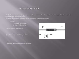
  • 1. PN JUNCTION DIODE Pn diode is a semiconducting device,that allow current to flow in one direction.it is a combination of two different types of semiconductor *pn diode is formed by joining acceptor impurities to donar impurities. where, p=donar impurity (+) n=acceptor impurity(-) *circuit symbol of pn diode: *graphical representatio of pn diode: * Electron & hole movement in pn diode:
  • 2. # To make current to flow through pn diode, "BIASING" of pn diode is done. there are two types of biasing .forward biasing .reverse biasing #FORWARD Biasing religion is connected to +ve terminal of eternal dc source & n religion is connected to -ve terminal. # REVERSE BAISING:N region is connected to +ve terminal of external dc source & p region is connected to -ve terminal. # The region in which only mobile ions & no free charge ions are present is called "DEPELTION LAYER"
  • 3. #Tthe minimum reverse voltage at which pn junction breakdown at certain rise in tempreature.Two types of breakdown are .....ZENER BREAKDOWN .....AVALANCHE BREAKDOWN #ZENER BREAKDOWN : it occurs due to heavy doping of p&n side of diode. deplition region is narrow in reverse biasing as,all the reverse voltage appears across the deplition layer. .in this breakdown electric feild is very intense across the deplition layer. .due to intnse e.f the covalent bond between electrons breaks &electron becomes free electrons. .a large number of such electrons constiuets a large reverse current this is known as” BREAKDOWN DUE TO ZENER EEFECT" #AVALANCHE BREAKDOWN:it occurs due to large reverse voltage applied to a diode, bywhich velocity of minority carrier increases therefore kinetic energy also increases. .then free electrons moves &passes this energy to the covalent bond electrons,due to which they jump to conduction bond for & become free for conduction .Now they knock out some more electrons from bond this series is known as"CHAIN REACTION"also as "AVALANCHE BREAKDOWN"
  • 4. *it is formed by joining forward & reverse characterstics of pn diode : *V(br) is the reverse breakdown voltage,the voltage at which breakdown occurs. *the reverse current I(0) upto V(br) is practically constant &neglegibly small. *diode current equation is : I(0) = I(0) [ e v/nT -1] where, I(0)=reversesaturation current, V(T)=T/11600 ;volt equivalent of tempreature. T=temp in kelvin,
  • 5. *effect of temp on pn diode is can be represented by: *I(0) i.e reverse saturatin current &V(T) i.e temp in kelvin is tempreature dependent due to which diode deoands on tempreature *by this graph :
  • 6. there are some special types of diode which are known as special purposediode. .zener diode .varactor diode .PIN diode .L**** ZENER DIODE : *it is a sepecil type of pn junction diode semiconductor diode.its construction is similar topn diode where breakdown voltage is adjusted between 3V to 200V. *doping of diode is controlled ,for proper function of diode. *circuit symbol of zener diode: *forward biasing of diode: *reverse biasing of diode: ed diode ** ZENER DIODE : *it is a sepecil type of pn junction diode semiconductor diode.its construction is similar to pn diode where breakdown voltage is adjusted between 3V to 200V *doping of diode is controlled ,for proper function of diode. *circuit symbol of zanier diode is: *forward biasing of diode: *reverse biasing of diode: .photo diode
  • 7. PIN DIODE
  • 8. VARACTOR DIODE
  • 9. LED DIODE
  • 10. PHOTO DIODE A photo diode is always operated at reverse biased condition. * circuit symbol of a photo diode *DARK CURRENT: current flowing through a photo diode in the absence of light. this current increases with increase in temperature. photo diode : *a photo diode is a highly sensitive diode & has high speed of operation as compared to led.