Downloaded 418 times


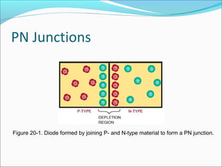
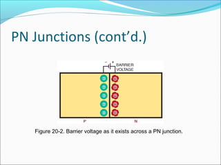
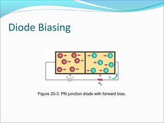

This document discusses PN junction diodes. It describes how a diode is formed by joining P-type and N-type semiconductor materials, creating a PN junction. The junction acts as a barrier that blocks current flow in one direction but allows it in the other. The document outlines diode biasing conditions and characteristics, including forward and reverse bias, and explains common diode construction techniques and testing methods using an ohmmeter.