Downloaded 91 times


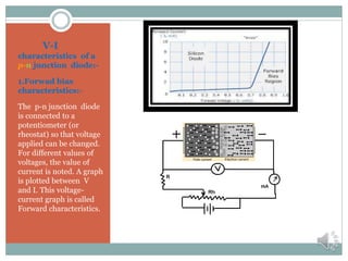


A p-n junction is formed where a single crystal of silicon or germanium is doped such that one half is p-type semiconductor and the other half is n-type semiconductor. When forward biased, the barrier potential decreases allowing majority charge carriers to flow across the junction, decreasing resistance. When reverse biased, the barrier potential increases preventing carrier flow and increasing resistance. The voltage-current characteristics of a p-n junction diode are nonlinear, with negligible current below the threshold voltage and exponential increase in current above it. In reverse bias, very little reverse saturation current flows until the breakdown voltage is exceeded.