Download to read offline

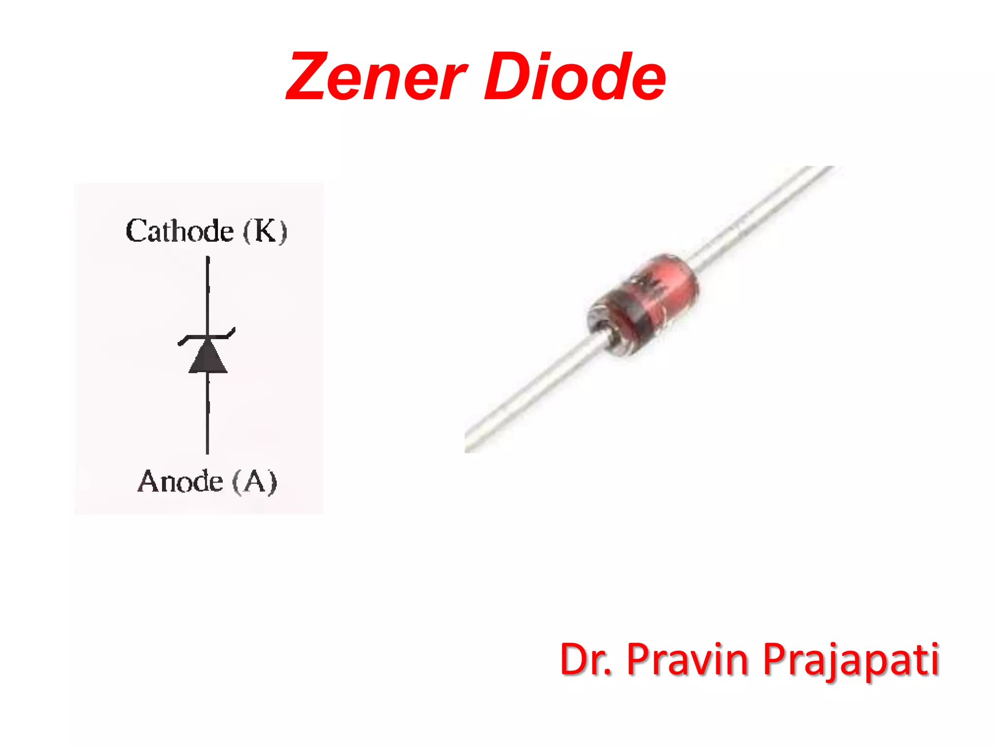

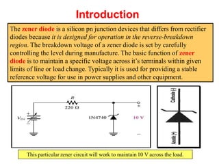
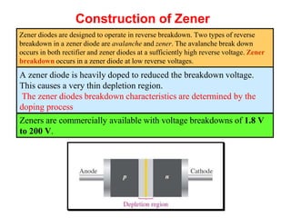
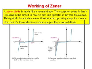
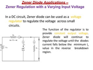
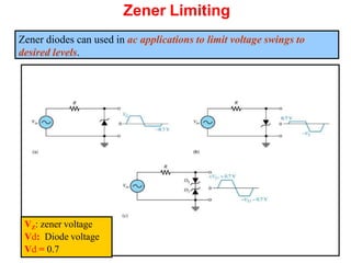


The document discusses the Zener diode, including its construction, working principle, and applications. A Zener diode is a pn junction device designed to operate in the reverse breakdown region and is used to regulate voltage. It breaks down at a specific voltage level set during manufacturing. Zener diodes regulate voltage by maintaining a constant voltage across their terminals despite variations in line or load. They are often used in power supplies and other equipment requiring a stable reference voltage.


