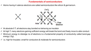
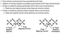
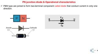
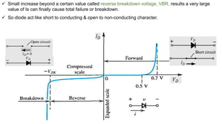
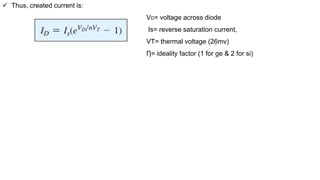
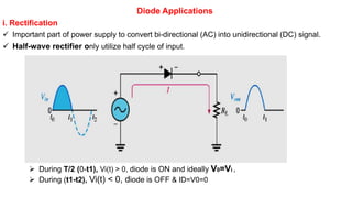
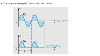
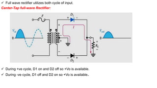
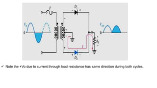
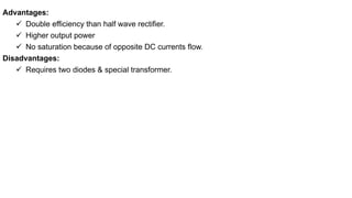
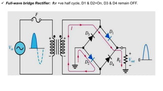
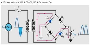
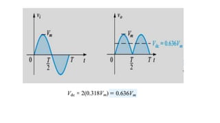
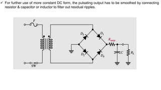
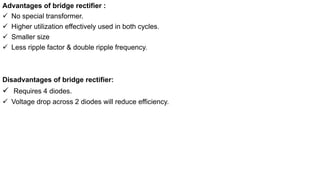
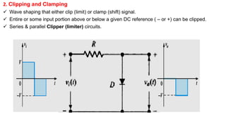
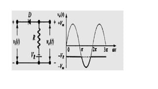
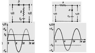
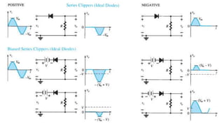
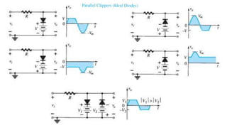
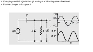
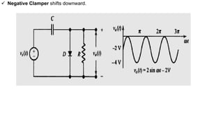
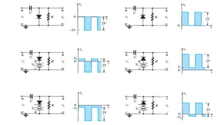
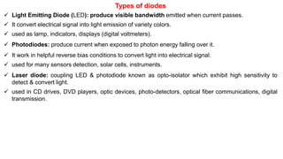
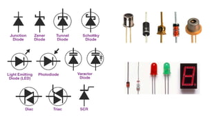
CHAPTER – TWO
Semiconductor diode and applications
 Semiconductors
 Biasing & Operation of Diode
 Applications
Fundamentals of semiconductors
 Atoms having 4 valence electrons are called semiconductors like silicon & germanium.
 At absolute 0 T, all electrons stay bonded so behaving as insulator.
 At high T, many electrons gaining sufficient energy will break the bond and freely move to able conduct.
 Minimum energy to dislodge no of electrons is a fundamental property of conductivity called band-gap
energy ( Eg).
 i.e. high for Insulator, small for conductors & moderate for semiconductors
 Pure intrinsic semiconductor has equal electrons & holes.
 Addition of impurity (dopant) is possible to get extrinsic N & P type semiconductor.
 N-type is created by doping pentavalent donor atom such as phosphorus.
 Electrons are majority carriers while holes are minority carriers.
 P-type is created by doping trivalent acceptor atoms such as boron.
 Holes are majority carriers while electrons are minority carries.
PN junction diode & Operational characteristics
 P&N type are joined to form two-terminal component called diode that conduct current in only one
direction.
 Initially, free electrons begin to migrate across the junction to fill up holes.
 Such back & forth continues until a built-in depletion barrier prevent any more crossing.
 Eventually, equal & opposite charged ions will create an electric field with +ve N-side & -ve P-side.
 Normally, potential difference of 0.6 - 0.7v for Si & 0.3 - 0.35 v for Ge will exist.
 Providing external voltage supplied between those two ends can give extra energy needed to overcome
the barrier.
 It is known as biasing which determine the diode character.
 Forward biased : Both majority carriers are forced to move creating a current flow, ID.
 ID becomes large quickly as VD increases beyond cut-in value of 0.3v (ge) & 0.6v(si).
 Reverse Biased : Very small drift current (Is) furtherly increase when VR increases.

 Small increase beyond a certain value called reverse breakdown voltage, VBR, results a very large
value of Is can finally cause total failure or breakdown.
 So diode act like short to conducting & open to non-conducting character.
 Thus, created current is:
VD= voltage across diode
Is= reverse saturation current,
VT= thermal voltage (26mv)
Ƞ= ideality factor (1 for ge & 2 for si)
Diode Applications
i. Rectification
 Important part of power supply to convert bi-directional (AC) into unidirectional (DC) signal.
 Half-wave rectifier only utilize half cycle of input.
 During T/2 (0-t1), Vi(t) > 0, diode is ON and ideally V0=Vi ,
 During (t1-t2), Vi(t) < 0, diode is OFF & ID=V0=0
 The output is average DC value , Vdc = 0.318 Vm
 Full wave rectifier utilizes both cycle of input.
Center-Tap full-wave Rectifier:
 During +ve cycle, D1 on and D2 off so +Vo is available.
 During -ve cycle, D1 off and D2 on so +Vo is available.
 Note the +Vo due to current through load resistance has same direction during both cycles.
Advantages:
 Double efficiency than half wave rectifier.
 Higher output power
 No saturation because of opposite DC currents flow.
Disadvantages:
 Requires two diodes & special transformer.
 Full-wave bridge Rectifier: for +ve half cycle, D1 & D2=On, D3 & D4 remain OFF.
 For -ve half cycle, D1 & D2=Off, D3 & D4 remain On.
 For further use of more constant DC form, the pulsating output has to be smoothed by connecting
resistor & capacitor or inductor to filter out residual ripples.
Advantages of bridge rectifier :
 No special transformer.
 Higher utilization effectively used in both cycles.
 Smaller size
 Less ripple factor & double ripple frequency.
Disadvantages of bridge rectifier:
 Requires 4 diodes.
 Voltage drop across 2 diodes will reduce efficiency.
2. Clipping and Clamping
 Wave shaping that either clip (limit) or clamp (shift) signal.
 Entire or some input portion above or below a given DC reference ( – or +) can be clipped.
 Series & parallel Clipper (limiter) circuits.
 Clamping can shift signals through adding or subtracting some offset level.
 Positive clamper shifts upward.
 Negative Clamper shifts downward.
Types of diodes
 Light Emitting Diode (LED): produce visible bandwidth emitted when current passes.
 It convert electrical signal into light emission of variety colors.
 used as lamp, indicators, displays (digital voltmeters).
 Photodiodes: produce current when exposed to photon energy falling over it.
 It work in helpful reverse bias conditions to convert light into electrical signal.
 used for many sensors detection, solar cells, instruments.
 Laser diode: coupling LED & photodiode known as opto-isolator which exhibit high sensitivity to
detect & convert light.
 used in CD drives, DVD players, optic devices, photo-detectors, optical fiber communications, digital
transmission.
 Zener Diodes : reversely operated to work in breakdown conditions & regulate a stable rating.
 used for power regulation, electronic stabilization of current and voltage.
 Schottky-barrier diode (SBD): has working voltage to perform at lower ranges(0.15 - 0.4).
 used in rectifier, digital fast switching.
 Varactor diode: provide voltage capacitance changed with preferred function.
 Used as variable capacitors in auto tuning of radio receivers.

Ch2-Diode.for electrical and computer engineering

  • 1.
    CHAPTER – TWO Semiconductordiode and applications  Semiconductors  Biasing & Operation of Diode  Applications
  • 2.
    Fundamentals of semiconductors Atoms having 4 valence electrons are called semiconductors like silicon & germanium.  At absolute 0 T, all electrons stay bonded so behaving as insulator.  At high T, many electrons gaining sufficient energy will break the bond and freely move to able conduct.  Minimum energy to dislodge no of electrons is a fundamental property of conductivity called band-gap energy ( Eg).  i.e. high for Insulator, small for conductors & moderate for semiconductors
  • 3.
     Pure intrinsicsemiconductor has equal electrons & holes.  Addition of impurity (dopant) is possible to get extrinsic N & P type semiconductor.  N-type is created by doping pentavalent donor atom such as phosphorus.  Electrons are majority carriers while holes are minority carriers.  P-type is created by doping trivalent acceptor atoms such as boron.  Holes are majority carriers while electrons are minority carries.
  • 4.
    PN junction diode& Operational characteristics  P&N type are joined to form two-terminal component called diode that conduct current in only one direction.
  • 5.
     Initially, freeelectrons begin to migrate across the junction to fill up holes.  Such back & forth continues until a built-in depletion barrier prevent any more crossing.  Eventually, equal & opposite charged ions will create an electric field with +ve N-side & -ve P-side.  Normally, potential difference of 0.6 - 0.7v for Si & 0.3 - 0.35 v for Ge will exist.  Providing external voltage supplied between those two ends can give extra energy needed to overcome the barrier.  It is known as biasing which determine the diode character.
  • 7.
     Forward biased: Both majority carriers are forced to move creating a current flow, ID.  ID becomes large quickly as VD increases beyond cut-in value of 0.3v (ge) & 0.6v(si).
  • 8.
     Reverse Biased: Very small drift current (Is) furtherly increase when VR increases. 
  • 9.
     Small increasebeyond a certain value called reverse breakdown voltage, VBR, results a very large value of Is can finally cause total failure or breakdown.  So diode act like short to conducting & open to non-conducting character.
  • 10.
     Thus, createdcurrent is: VD= voltage across diode Is= reverse saturation current, VT= thermal voltage (26mv) Ƞ= ideality factor (1 for ge & 2 for si)
  • 11.
    Diode Applications i. Rectification Important part of power supply to convert bi-directional (AC) into unidirectional (DC) signal.  Half-wave rectifier only utilize half cycle of input.  During T/2 (0-t1), Vi(t) > 0, diode is ON and ideally V0=Vi ,  During (t1-t2), Vi(t) < 0, diode is OFF & ID=V0=0
  • 12.
     The outputis average DC value , Vdc = 0.318 Vm
  • 13.
     Full waverectifier utilizes both cycle of input. Center-Tap full-wave Rectifier:  During +ve cycle, D1 on and D2 off so +Vo is available.  During -ve cycle, D1 off and D2 on so +Vo is available.
  • 14.
     Note the+Vo due to current through load resistance has same direction during both cycles.
  • 15.
    Advantages:  Double efficiencythan half wave rectifier.  Higher output power  No saturation because of opposite DC currents flow. Disadvantages:  Requires two diodes & special transformer.
  • 16.
     Full-wave bridgeRectifier: for +ve half cycle, D1 & D2=On, D3 & D4 remain OFF.
  • 17.
     For -vehalf cycle, D1 & D2=Off, D3 & D4 remain On.
  • 19.
     For furtheruse of more constant DC form, the pulsating output has to be smoothed by connecting resistor & capacitor or inductor to filter out residual ripples.
  • 20.
    Advantages of bridgerectifier :  No special transformer.  Higher utilization effectively used in both cycles.  Smaller size  Less ripple factor & double ripple frequency. Disadvantages of bridge rectifier:  Requires 4 diodes.  Voltage drop across 2 diodes will reduce efficiency.
  • 21.
    2. Clipping andClamping  Wave shaping that either clip (limit) or clamp (shift) signal.  Entire or some input portion above or below a given DC reference ( – or +) can be clipped.  Series & parallel Clipper (limiter) circuits.
  • 26.
     Clamping canshift signals through adding or subtracting some offset level.  Positive clamper shifts upward.
  • 27.
     Negative Clampershifts downward.
  • 29.
    Types of diodes Light Emitting Diode (LED): produce visible bandwidth emitted when current passes.  It convert electrical signal into light emission of variety colors.  used as lamp, indicators, displays (digital voltmeters).  Photodiodes: produce current when exposed to photon energy falling over it.  It work in helpful reverse bias conditions to convert light into electrical signal.  used for many sensors detection, solar cells, instruments.  Laser diode: coupling LED & photodiode known as opto-isolator which exhibit high sensitivity to detect & convert light.  used in CD drives, DVD players, optic devices, photo-detectors, optical fiber communications, digital transmission.
  • 31.
     Zener Diodes: reversely operated to work in breakdown conditions & regulate a stable rating.  used for power regulation, electronic stabilization of current and voltage.  Schottky-barrier diode (SBD): has working voltage to perform at lower ranges(0.15 - 0.4).  used in rectifier, digital fast switching.  Varactor diode: provide voltage capacitance changed with preferred function.  Used as variable capacitors in auto tuning of radio receivers.