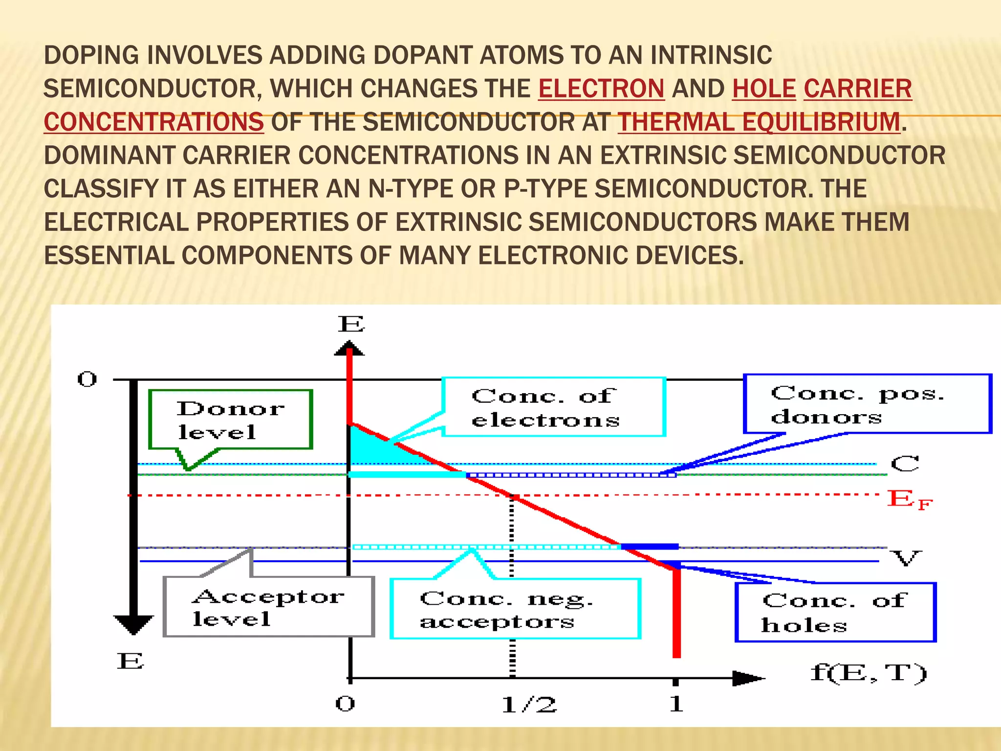
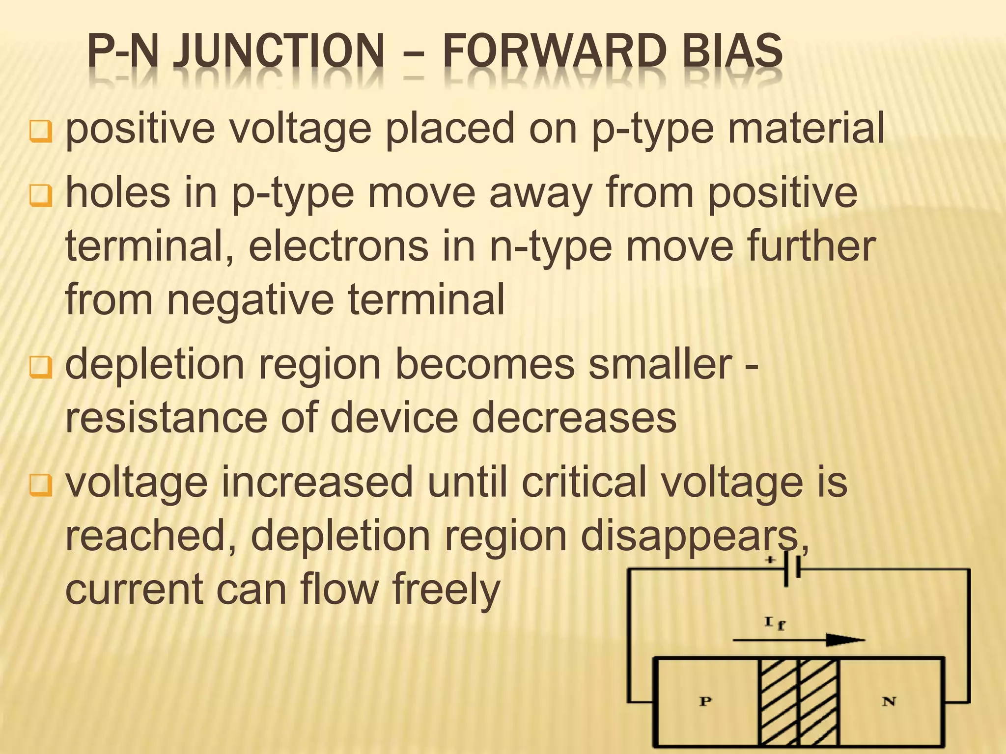
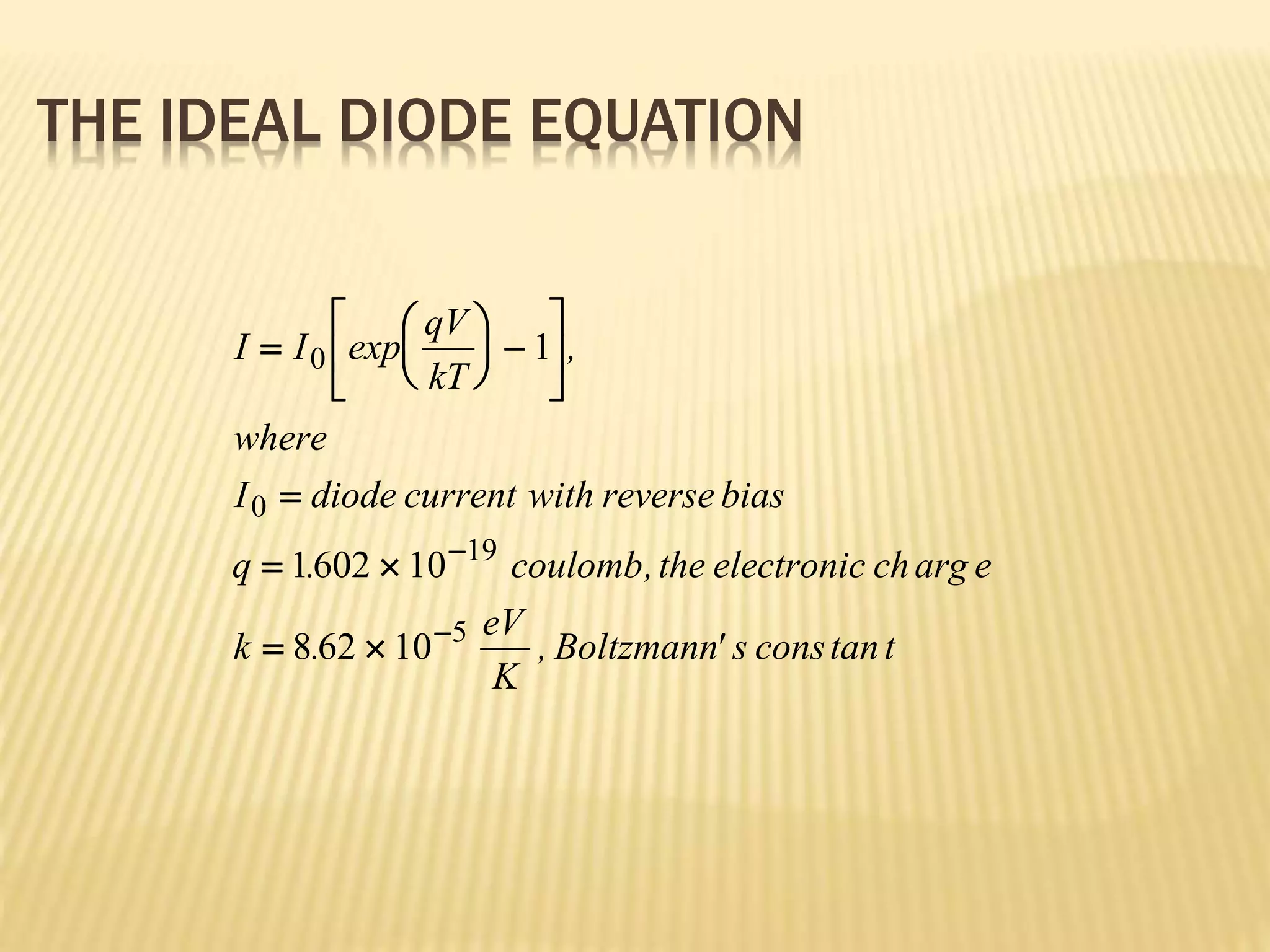
OBJECTIVE
 Energy band and energy band gap
 Classification of materials on the basis of
energy band gap
 What is Semiconductor
 Types of semiconductor
 Extrinsic semiconductor
 Semiconductor junction
 Semiconductor device (P-N DIODE)
 Applications of diode
DIFFERENCE BETWEEN
CONDUCTORS,INSULATORS,SEMICONDUCTORS
 Energy band & energy band gap:-
 Each isolated atom has a discrete
energy level. But in general isolated atoms are not exist .they
exist in the form of crystal. In that crystal there are nearby atoms
,which also have an energy level nearly equal to the previous
energy level.
so these “closely spaced energy levels form a band
of energy” called energy band.
 valance band is located blow the conduction band eperated from
it by a energy band gap.
• In conductors C.B. and V.B. are overlapped
• In insulators energy band gap is 6eV
• In semiconductors energy band gap is 1eV
CLASSIFICATION OF MATERIALS ON THE BASIS
OF ENERGY BAND GAP
 Coductors
 Insulators
 Semiconductors
SEMICONDUCTOR
 Semiconductor are those materials which
behaves like insulators at 0 degree Celsius
and like conductor at room temperature.
 They have properties between conductors
and insulators.
TYPES OF SEMICONDUCTOR
 Intrinsic semiconductors:-
Intrinsic semiconductors are
pure semiconductors, no impurities are added
in these conductors.
So the no. of free electrons and holes are
equal . Conductivity of these semiconductors is
low because of electrons are in perfect
covalent bonding.
 Extrinsic semiconductors
INTRINSIC (PURE) SILICON
At 0 Kelvin Silicon density is
5*10²³particles/cm³
Silicon has 4 valence electrons, it
covalently bonds with four adjacent
atoms in the crystal lattice
Higher temperatures create free
charge carriers.
A “hole” is created in the absence of
an electron.
At 23C there are 10¹º particles/cm³ of
free carriers
EXTRINSIC SEMICONDUCTORS
An extrinsic semiconductor is a semiconductor that
has been doped, that is, into which a doping agent has
been introduced, giving it different electrical properties
than theintrinsic (pure) semiconductor.
DOPING INVOLVES ADDING DOPANT ATOMS TO AN INTRINSIC
SEMICONDUCTOR, WHICH CHANGES THE ELECTRON AND HOLE CARRIER
CONCENTRATIONS OF THE SEMICONDUCTOR AT THERMAL EQUILIBRIUM.
DOMINANT CARRIER CONCENTRATIONS IN AN EXTRINSIC SEMICONDUCTOR
CLASSIFY IT AS EITHER AN N-TYPE OR P-TYPE SEMICONDUCTOR. THE
ELECTRICAL PROPERTIES OF EXTRINSIC SEMICONDUCTORS MAKE THEM
ESSENTIAL COMPONENTS OF MANY ELECTRONIC DEVICES.
TYPES OF EXTRINSIC SEMICONDUCTOR
 P type
 N type
P-TYPE N-TYPE
 When a doped
semiconductor
contains excess holes
it is called P-type
semiconductor.
 Doping is
trivalent,B,Ga,In,Al
 When a dped
semiconductor contains
excess electrons it is
called N-type
semiconductor.
 Doping is
pentavalent,As,Bi,Sb,P
DOPING
The N in N-type stands for negative.
A column V ion is inserted.
The extra valence electron is free to
move about the lattice
There are two types of doping
N-type and P-type.
The P in P-type stands for positive.
A column III ion is inserted.
Electrons from the surrounding
Silicon move to fill the “hole.”
CRYSTALLINE NATURE OF SILICON
 Silicon as utilized in integrated circuits is
crystalline in nature
 As with all crystalline material, silicon
consists of a repeating basic unit structure
called a unit cell
 For silicon, the unit cell consists of an atom
surrounded by four equidistant nearest
neighbors which lie at the corners of the
tetrahedron
P-N JUNCTION
 Also known as a diode
 One of the basics of semiconductor
technology -
 Created by placing n-type and p-type
material in close contact
 Diffusion - mobile charges (holes) in p-
type combine with mobile charges
(electrons) in n-type
P-N JUNCTION
 Region of charges left behind (dopants
fixed in crystal lattice)
 Group III in p-type (one less proton than Si-
negative charge)
 Group IV in n-type (one more proton than
Si - positive charge)
 Region is totally depleted of mobile
charges - “depletion region”
 Electric field forms due to fixed charges in
the depletion region
 Depletion region has high resistance due
to lack of mobile charges
THE P-N JUNCTION
THE JUNCTION

The “potential” or voltage across the silicon
changes in the depletion region and goes from
+ in the n region to – in the p region
BIASING THE P-N DIODE
Forward Bias
Applies - voltage
to the n region and
+ voltage to the p
region
CURRENT!
Reverse Bias
Applies + voltage
to n region and –
voltage to p region
NO CURRENT
THINK OF THE DIODE
AS A SWITCH
P-N JUNCTION – REVERSE BIAS
 positive voltage placed on n-type
material
 electrons in n-type move closer to
positive terminal, holes in p-type move
closer to negative terminal
 width of depletion region increases
 allowed current is essentially zero
(small “drift” current)
P-N JUNCTION – FORWARD BIAS
 positive voltage placed on p-type material
 holes in p-type move away from positive
terminal, electrons in n-type move further
from negative terminal
 depletion region becomes smaller -
resistance of device decreases
 voltage increased until critical voltage is
reached, depletion region disappears,
current can flow freely
P-N JUNCTION - V-I CHARACTERISTICS
Voltage-Current relationship for a p-n junction (diode)
CURRENT-VOLTAGE CHARACTERISTICS
THE IDEAL DIODE
Positive voltage yields finite
current
Negative voltage yields zero
current REAL DIODE
I I
qV
kT
where
I diode current with reverse bias
q coulomb the electronic ch e
k
eV
K
Boltzmann s cons t






 







 
 


0
0
19
5
1
1602 10
8 62 10
exp ,
. , arg
. , ' tan
THE IDEAL DIODE EQUATION
SEMICONDUCTOR DIODE - OPENED REGION
 The p-side is the cathode, the n-side is the anode
 The dropped voltage, VD is measured from the
cathode to the anode
 Opened: VD  VF:
VD = VF
ID = circuit limited, in our model the VD cannot exceed
VF
SEMICONDUCTOR DIODE - CUT-OFF REGION
 Cut-off: 0 < VD < VF:
ID  0 mA
SEMICONDUCTOR DIODE - CLOSED REGION
 Closed: VF < VD  0:
 VD is determined by the circuit, ID
= 0 mA
 Typical values of VF: 0.5 ¸ 0.7 V
ZENER EFFECT
 Zener break down: VD <= VZ:
VD = VZ, ID is determined by the circuit.
 In case of standard diode the typical values of the
break down voltage VZ of the Zener effect -20 ... -
100 V
 Zener diode
 Utilization of the Zener effect
 Typical break down values of VZ : -4.5 ... -15 V
LED
 Light emitting diode, made from GaAs
 VF=1.6 V
 IF >= 6 mA
Semiconductor diodes

Semiconductor diodes

  • 2.
    OBJECTIVE  Energy bandand energy band gap  Classification of materials on the basis of energy band gap  What is Semiconductor  Types of semiconductor  Extrinsic semiconductor  Semiconductor junction  Semiconductor device (P-N DIODE)  Applications of diode
  • 3.
    DIFFERENCE BETWEEN CONDUCTORS,INSULATORS,SEMICONDUCTORS  Energyband & energy band gap:-  Each isolated atom has a discrete energy level. But in general isolated atoms are not exist .they exist in the form of crystal. In that crystal there are nearby atoms ,which also have an energy level nearly equal to the previous energy level. so these “closely spaced energy levels form a band of energy” called energy band.  valance band is located blow the conduction band eperated from it by a energy band gap. • In conductors C.B. and V.B. are overlapped • In insulators energy band gap is 6eV • In semiconductors energy band gap is 1eV
  • 4.
    CLASSIFICATION OF MATERIALSON THE BASIS OF ENERGY BAND GAP  Coductors  Insulators  Semiconductors
  • 5.
    SEMICONDUCTOR  Semiconductor arethose materials which behaves like insulators at 0 degree Celsius and like conductor at room temperature.  They have properties between conductors and insulators.
  • 6.
    TYPES OF SEMICONDUCTOR Intrinsic semiconductors:- Intrinsic semiconductors are pure semiconductors, no impurities are added in these conductors. So the no. of free electrons and holes are equal . Conductivity of these semiconductors is low because of electrons are in perfect covalent bonding.  Extrinsic semiconductors
  • 7.
    INTRINSIC (PURE) SILICON At0 Kelvin Silicon density is 5*10²³particles/cm³ Silicon has 4 valence electrons, it covalently bonds with four adjacent atoms in the crystal lattice Higher temperatures create free charge carriers. A “hole” is created in the absence of an electron. At 23C there are 10¹º particles/cm³ of free carriers
  • 8.
    EXTRINSIC SEMICONDUCTORS An extrinsicsemiconductor is a semiconductor that has been doped, that is, into which a doping agent has been introduced, giving it different electrical properties than theintrinsic (pure) semiconductor.
  • 9.
    DOPING INVOLVES ADDINGDOPANT ATOMS TO AN INTRINSIC SEMICONDUCTOR, WHICH CHANGES THE ELECTRON AND HOLE CARRIER CONCENTRATIONS OF THE SEMICONDUCTOR AT THERMAL EQUILIBRIUM. DOMINANT CARRIER CONCENTRATIONS IN AN EXTRINSIC SEMICONDUCTOR CLASSIFY IT AS EITHER AN N-TYPE OR P-TYPE SEMICONDUCTOR. THE ELECTRICAL PROPERTIES OF EXTRINSIC SEMICONDUCTORS MAKE THEM ESSENTIAL COMPONENTS OF MANY ELECTRONIC DEVICES.
  • 10.
    TYPES OF EXTRINSICSEMICONDUCTOR  P type  N type
  • 11.
    P-TYPE N-TYPE  Whena doped semiconductor contains excess holes it is called P-type semiconductor.  Doping is trivalent,B,Ga,In,Al  When a dped semiconductor contains excess electrons it is called N-type semiconductor.  Doping is pentavalent,As,Bi,Sb,P
  • 12.
    DOPING The N inN-type stands for negative. A column V ion is inserted. The extra valence electron is free to move about the lattice There are two types of doping N-type and P-type. The P in P-type stands for positive. A column III ion is inserted. Electrons from the surrounding Silicon move to fill the “hole.”
  • 13.
    CRYSTALLINE NATURE OFSILICON  Silicon as utilized in integrated circuits is crystalline in nature  As with all crystalline material, silicon consists of a repeating basic unit structure called a unit cell  For silicon, the unit cell consists of an atom surrounded by four equidistant nearest neighbors which lie at the corners of the tetrahedron
  • 15.
    P-N JUNCTION  Alsoknown as a diode  One of the basics of semiconductor technology -  Created by placing n-type and p-type material in close contact  Diffusion - mobile charges (holes) in p- type combine with mobile charges (electrons) in n-type
  • 16.
    P-N JUNCTION  Regionof charges left behind (dopants fixed in crystal lattice)  Group III in p-type (one less proton than Si- negative charge)  Group IV in n-type (one more proton than Si - positive charge)  Region is totally depleted of mobile charges - “depletion region”  Electric field forms due to fixed charges in the depletion region  Depletion region has high resistance due to lack of mobile charges
  • 17.
  • 18.
    THE JUNCTION  The “potential”or voltage across the silicon changes in the depletion region and goes from + in the n region to – in the p region
  • 19.
    BIASING THE P-NDIODE Forward Bias Applies - voltage to the n region and + voltage to the p region CURRENT! Reverse Bias Applies + voltage to n region and – voltage to p region NO CURRENT THINK OF THE DIODE AS A SWITCH
  • 20.
    P-N JUNCTION –REVERSE BIAS  positive voltage placed on n-type material  electrons in n-type move closer to positive terminal, holes in p-type move closer to negative terminal  width of depletion region increases  allowed current is essentially zero (small “drift” current)
  • 21.
    P-N JUNCTION –FORWARD BIAS  positive voltage placed on p-type material  holes in p-type move away from positive terminal, electrons in n-type move further from negative terminal  depletion region becomes smaller - resistance of device decreases  voltage increased until critical voltage is reached, depletion region disappears, current can flow freely
  • 22.
    P-N JUNCTION -V-I CHARACTERISTICS Voltage-Current relationship for a p-n junction (diode)
  • 23.
    CURRENT-VOLTAGE CHARACTERISTICS THE IDEALDIODE Positive voltage yields finite current Negative voltage yields zero current REAL DIODE
  • 24.
    I I qV kT where I diodecurrent with reverse bias q coulomb the electronic ch e k eV K Boltzmann s cons t                      0 0 19 5 1 1602 10 8 62 10 exp , . , arg . , ' tan THE IDEAL DIODE EQUATION
  • 25.
    SEMICONDUCTOR DIODE -OPENED REGION  The p-side is the cathode, the n-side is the anode  The dropped voltage, VD is measured from the cathode to the anode  Opened: VD  VF: VD = VF ID = circuit limited, in our model the VD cannot exceed VF
  • 26.
    SEMICONDUCTOR DIODE -CUT-OFF REGION  Cut-off: 0 < VD < VF: ID  0 mA SEMICONDUCTOR DIODE - CLOSED REGION  Closed: VF < VD  0:  VD is determined by the circuit, ID = 0 mA  Typical values of VF: 0.5 ¸ 0.7 V
  • 27.
    ZENER EFFECT  Zenerbreak down: VD <= VZ: VD = VZ, ID is determined by the circuit.  In case of standard diode the typical values of the break down voltage VZ of the Zener effect -20 ... - 100 V  Zener diode  Utilization of the Zener effect  Typical break down values of VZ : -4.5 ... -15 V
  • 28.
    LED  Light emittingdiode, made from GaAs  VF=1.6 V  IF >= 6 mA