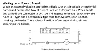
CBCS:E1-Unit-2PPT
Junction diode and its Applications
Pn-Junction diode: A semiconductor diode is a two terminal electronic
component with a PN junction. This is also called as a Rectifier.
The anode which is the positive terminal of a diode is represented
with A and the cathode, which is the negative terminal is represented
with K. To know the anode and cathode of a practical diode, a fine line
is drawn on the diode which means cathode, while the other end
represents anode.
As we had already discussed about the P-type and N-type
semiconductors, and the behavior of their carriers, let us now try to join
these materials together to see what happens.
Formation of a Diode:
If a P-type and an N-type material are brought close to each other, both
of them join to form a junction, as shown in the figure below.
A P-type material has holes as the majority carriers and an N-type
material has electrons as the majority carriers. As opposite charges
attract, few holes in P-type tend to go to n-side, whereas few
electrons in N-type tend to go to P-side.
As both of them travel towards the junction, holes and electrons recombine
with each other to neutralize and forms ions. Now, in this junction, there exists
a region where the positive and negative ions are formed, called as PN junction
or junction barrier as shown in the figure.
The formation of negative ions on P-side and positive ions on N-side results in
the formation of a narrow charged region on either side of the PN junction.
This region is now free from movable charge carriers. The ions present here
have been stationary and maintain a region of space between them without
any charge carriers.
As this region acts as a barrier between P and N type materials, this is also
called as Barrier junction. This has another name called as Depletion region
meaning it depletes both the regions. There occurs a potential difference VD
due to the formation of ions, across the junction called as Potential Barrier as
it prevents further movement of holes and electrons through the junction.
Biasing of a Diode :
When a diode or any two-terminal component is connected in a circuit, it has
two biased conditions with the given supply. They are Forward biased
condition and Reverse biased condition. Let us know them in detail.
Forward Biased Condition :
When a diode is connected in a circuit, with its anode to the positive terminal
and cathode to the negative terminal of the supply, then such a connection is
said to be forward biased condition. This kind of connection makes the circuit
more and more forward biased and helps in more conduction. A diode
conducts well in forward biased condition.
Reverse Biased Condition :
When a diode is connected in a circuit, with its anode to the negative terminal
and cathode to the positive terminal of the supply, then such a connection is
said to be Reverse biased condition. This kind of connection makes the circuit
more and more reverse biased and helps in minimizing and preventing the
conduction. A diode cannot conduct in reverse biased condition.
Let us now try to know what happens if a diode is connected in forward
biased and in reverse biased conditions.
Working under Forward Biased :
When an external voltage is applied to a diode such that it cancels the potential
barrier and permits the flow of current is called as forward bias. When anode
and cathode are connected to positive and negative terminals respectively, the
holes in P-type and electrons in N-type tend to move across the junction,
breaking the barrier. There exists a free flow of current with this, almost
eliminating the barrier.
With the repulsive force provided by positive terminal to holes and by negative
terminal to electrons, the recombination takes place in the junction. The supply
voltage should be such high that it forces the movement of electrons and holes
through the barrier and to cross it to provide forward current.
Forward Current is the current produced by the diode when operating in
forward biased condition and it is indicated by If.
Working under Reverse Biased :When an external voltage is applied to a diode
such that it increases the potential barrier and restricts the flow of current is
called as Reverse bias. When anode and cathode are connected to negative and
positive terminals respectively, the electrons are attracted towards the positive
terminal and holes are attracted towards the negative terminal. Hence both will
be away from the potential barrier increasing the junction resistance and
preventing any electron to cross the junction.The following figure explains this.
The graph of conduction when no field is applied and when some external field
is applied are also drawn.
With the increasing reverse bias, the junction has few minority carriers to cross
the junction. This current is normally negligible. This reverse current is almost
constant when the temperature is constant. But when this reverse voltage
increases further, then a point called reverse breakdown occurs, where an
avalanche of current flows through the junction. This high reverse current
damages the device.
Reverse current is the current produced by the diode when operating in
reverse biased condition and it is indicated by Ir. Hence a diode provides high
resistance path in reverse biased condition and doesn’t conduct, where it
provides a low resistance path in forward biased condition and conducts. Thus
we can conclude that a diode is a one-way device which conducts in forward
bias and acts as an insulator in reverse bias. This behavior makes it work as a
rectifier, which converts AC to DC.
Peak Inverse Voltage :
Peak Inverse Voltage is shortly called as PIV. It states the maximum voltage
applied in reverse bias. The Peak Inverse Voltage can be defined as “The
maximum reverse voltage that a diode can withstand without being
destroyed”. Hence, this voltage is considered during reverse biased condition. It
denotes how a diode can be safely operated in reverse bias.
Purpose of a Diode
A diode is used to block the electric current flow in one direction, i.e. in forward
direction and to block in reverse direction. This principle of diode makes it work
as a Rectifier.
For a circuit to allow the current flow in one direction but to stop in the other
direction, the rectifier diode is the best choice. Thus the output will be DC
removing the AC components. The circuits such as half wave and full wave
rectifiers are made using diodes, which can be studied in Electronic Circuits
tutorials.
A diode is also used as a Switch. It helps a faster ON and OFF for the output that
should occur in a quick rate.
V - I Characteristics of a Diode :
A Practical circuit arrangement for a PN junction diode is as shown in the
following figure. An ammeter is connected in series and voltmeter in parallel,
while the supply is controlled through a variable resistor.
During the operation, when the diode is in forward biased condition, at some
particular voltage, the potential barrier gets eliminated. Such a voltage is
called as Cut-off Voltage or Knee Voltage. If the forward voltage exceeds
beyond the limit, the forward current rises up exponentially and if this is done
further, the device is damaged due to overheating.
The following graph shows the state of diode conduction in forward and
reverse biased conditions.
During the reverse bias, current produced through minority carriers exist
known as “Reverse current”. As the reverse voltage increases, this reverse
current increases and it suddenly breaks down at a point, resulting in the
permanent destruction of the junction.
Types of Junction diodes :
The junction diodes are the normal PN junction diodes but differ in
construction. There are three types of junction diodes, as shown in the
following figure.
Rectifier Diode :
These diodes are the normal PN junction diodes, which allow current to flow
through them in only one direction and stop in the other direction. These
diodes are used in rectifier circuits to convert alternating current into direct
current.
In the above figure, we can see the same rectifier diodes with a metal
projection. This is added to the diode to minimize the heat distribution which
might affect the diode sometimes. Such a metal projection is called as Heat sink.
These help in the improvement of the diode performance and the diodes will be
able to withstand high powers, without getting affected.
There are circuits such as Half wave rectifier and Full wave rectifier circuits which
use these diodes. These circuits are discussed in ELECTRONIC CIRCUITS tutorial.
These rectifier circuits are used in Power supply sections of many circuits where
alternating input current has to be converted into direct current for that circuit
applications.
Zener Diode :
This is a special kind of diode which permits current flow not only in forward
direction, but also in reverse direction. A normal diode, when operated in
reverse bias, gets damaged if the reverse current above a certain value is
passed through it. This “certain value” is called as the Breakdown voltage.
The breakdown voltage of a Zener diode is very low. But this diode allows the
reverse current to pass through it, once this breakdown voltage is exceeded.
That breakdown voltage is called as Zener Voltage. Hence there is a controlled
breakdown which does not damage the diode when a reverse current above
the Zener voltage passes through a Zener diode.
A Zener diode in its reverse bias, exhibits a controlled breakdown voltage and it
allows the current flow to keep the value of voltage across that Zener diode
close to the Zener breakdown voltage value. This value of Zener breakdown
voltage makes any Zener diode to be chosen for certain applications.
Avalanche diode is another diode which has the similar characteristics of Zener
diode. The avalanche breakdown takes place across the entire PN junction,
when the voltage drop is constant and is independent of current. This avalanche
diode is used for photo detection.
V-I Characteristics of a Zener diode : The V-I Characteristics of a Zener diode
are common for any diode when operated in forward bias. But the reverse bias
operation of a Zener diode makes it very important to consider. Let us have a
look at the graph.
The point where the bent is shown in the reverse bias operation, is the Zener
breakdown voltage, after which the diode allows high reverse currents through
it.
This Zener voltage is indicated by VZ. This incredible quality of Zener diode
made it the most reliable one and have got many applications too.
Applications of Zener diode : This diode has many applications such as − It is
mostly used as a Voltage Regulator. Provides fixed reference voltage in transistor
biasing circuits. For peak clipping or limiting in wave shaping circuits. As a Surge
protector in many circuits. For meter protection against damage from accidental
applications.
Switching Diode :This is a normal single PN junction diode which is especially
designed for switching purposes. This diode can exhibit two states of high and
low resistance clearly which can be used alternatively.
The junction capacitance of this diode is made very low so as to minimize other
effects. The switching speed is made quite high. When the diode has high
resistance it works as an open switch and it acts as a closed switch during low
resistance. This transition occurs at a faster rate in switching diode, than in any
ordinary one.
Applications of switching diode : These have many applications such as −
Used in high-speed rectifying circuits , Used in ring modulators , Used in radio
frequency receivers , Used as reverse polarity protectors
Used for both General purpose and high speed switching applications
There are few diodes which are designed to serve some special purposes.
There are many of such kinds like Transient voltage suppression diodes, Gold
doped diodes, Super barrier diodes, Point contact diodes, Peltier diodes etc.
But other than these, there are few prominent diodes, which have got many
applications.
Rectifiers :
A simple PN junction diode acts as a rectifier. The forward biasing and reverse
biasing conditions of the diode makes the rectification.
Rectification :
An alternating current has the property to change its state continuously. This is
understood by observing the sine wave by which an alternating current is
indicated. It raises in its positive direction goes to a peak positive value, reduces
from there to normal and again goes to negative portion and reaches the
negative peak and again gets back to normal and goes on.
During its journey in the formation of wave, we can observe that the wave goes
in positive and negative directions. Actually it alters completely and hence the
name alternating current.
But during the process of rectification, this alternating current is changed into
direct current DC. The wave which flows in both positive and negative direction
till then, will get its direction restricted only to positive direction, when
converted to DC. Hence the current is allowed to flow only in positive direction
and resisted in negative direction, just as in the figure below.
The circuit which does rectification is called as a Rectifier circuit. A diode is
used as a rectifier, to construct a rectifier circuit.
Types of Rectifier circuits
There are two main types of rectifier circuits, depending upon their output.
They are : Half-wave Rectifier , Full-wave Rectifier
A Half-wave rectifier circuit rectifies only positive half cycles of the input
supply whereas a Full-wave rectifier circuit rectifies both positive and negative
half cycles of the input supply.
Half-Wave Rectifier :
The name half-wave rectifier itself states that the rectification is done only for
half of the cycle. The AC signal is given through an input transformer which
steps up or down according to the usage. Mostly a step down transformer is
used in rectifier circuits, so as to reduce the input voltage.
The input signal given to the transformer is passed through a PN junction
diode which acts as a rectifier.
This diode converts the AC voltage into pulsating dc for only the positive half
cycles of the input. A load resistor is connected at the end of the circuit. The
figure below shows the circuit of a half wave rectifier.
Working of a HWR :The input signal is given to the transformer which reduces
the voltage levels. The output from the transformer is given to the diode which
acts as a rectifier. This diode gets ON conducts for positive half cycles of input
signal. Hence a current flows in the circuit and there will be a voltage drop
across the load resistor. The diode gets OFF doesn′tconduct for negative half
cycles and hence the output for negative half cycles will be, iD=0 and Vo=0.
Hence the output is present for positive half cycles of the input voltage only
neglecting the reverse leakage current. This output will be pulsating which is
taken across the load resistor.
Waveforms of a HWR
The input and output waveforms are as shown in the following figure.
Hence the output of a half wave rectifier is a pulsating dc. Let us try to analyze
the above circuit by understanding few values which are obtained from the
output of half wave rectifier.
Analysis of Half-Wave Rectifier:
To analyze a half-wave rectifier circuit, let us consider the equation of input
voltage. vi=Vm sinωt
Vm is the maximum value of supply voltage.
Let us assume that the diode is ideal.
The resistance in the forward direction, i.e., in the ON state is Rf.
The resistance in the reverse direction, i.e., in the OFF state is Rr.
The current i in the diode or the load resistor RL is given by
i=Im sinωt for 0 ≤ ωt ≤ 2π
i=0forπ≤ωt≤2π
Where
Im=Vm/ (Rf+RL)
DC Output Current
The average current Idc is given by
Idc=1/2π∫2π0 I d(ωt)
=1/2π[∫π0 Im sinωt d(ωt)+∫2π0 0d(ωt)]
=1/2π[Im{−cosωt}π0]
=1/2π[Im{+1−(−1)}]=Im/π=0.318 Im
Substituting the value of Im, we get
Idc=Vm/π(Rf+RL)
If RL>>Rf, then
Idc=(Vm/π)RL=0.318(Vm/RL)
DC Output Voltage: The DC output voltage is given by
Vdc=Idc×RL=(Im/π)×RL
=(Vm×RL)/π(Rf+RL)=Vm/π{1+(Rf/RL)}
If RL>>Rf, then , Vdc=Vm/π=0.318Vm
RMS Current and Voltage
The value of RMS current is given by
Irms=[1/2π∫2π0(i)sq.d(ωt)]powerhalf.
Irms=[1/2π∫2π0(Im)sq.sin2ωtd(ωt)+1/2π∫2ππ0d(ωt)]12
=[I2m/2π∫π0(1−cos2ωt2)d(ωt)]12
=[I2m/4π{(ωt)−sin2ωt2}π0]12
=[I2m/4π{π−0−sin2π2+sin0}]12
=[I2m/4π]12=Im/2
=Vm/2(Rf+RL)
RMS voltage across the load is
Vrms=Irms×RL=Vm×RL/2(Rf+RL)
=Vm/2{1+(Rf/RL)}
If RL>>Rf, then
Vrms=Vm/2
Rectifier Efficiency:
Any circuit needs to be efficient in its working for a better output. To calculate
the efficiency of a half wave rectifier, the ratio of the output power to the input
power has to be considered.
The rectifier efficiency is defined as
η=d.c.powerdelivered to the load a.c.input power from transformer
secondary=Pac Pdc
Now Pdc=(Idc)2×RL=ImRL/π2
Further Pac=Pa+Pr
Where Pa=powerdissipatedatthejunctionofdiode
=I2rms×Rf=I2m/4×Rf And
Pr=powerdissipatedintheloadresistance
=I2rms×RL=I2m4×RL
Pac=I2m4×Rf+I2m4×RL=I2m4(Rf+RL)
From both the expressions of Pac and Pdc,
we can write
η=I2mRL/π2I2m(Rf+RL)/4=4π2RL(Rf+RL)
=4π21{1+(Rf/RL)}=0.406{1+(Rf/RL)}
Percentage rectifier efficiency
η=40.6{1+⟮Rf/RL⟯}
Theoretically, the maximum value of rectifier efficiency of a half wave rectifier
is 40.6% when Rf/RL=0
Further, the efficiency may be calculated in the following way
η=Pdc/Pac=(Idc)2RL/(Irms)2RL=(Vdc/RL)2RL/(Vrms/RL)2RL=(Vdc)2/(Vrms)2
=(Vm/π)2/(Vm/2)2=4π2=0.406
=40.6%
Ripple Factor:
The rectified output contains some amount of AC component present in it, in the
form of ripples. This is understood by observing the output waveform of the half
wave rectifier. To get a pure dc, we need to have an idea on this component.
The ripple factor gives the waviness of the rectified output. It is denoted by y. This
can be defined as the ratio of the effective value of ac component of voltage or
current to the direct value or average value.
γ=ripple voltage d.c voltage=rms value of a.c.component
d.c.valueofwave=(Vr)rmsvdc
Here,
(Vr)rms=V2rms−V2dc−−−−−−−−√
Therefore,
γ=V2rms−V2dc−−−−−−−−√Vdc=(VrmsVdc)2−1−−−−−−−−−−−√
Now, Vrms=[12π∫2π0V2msin2ωtd(ωt)]12
=Vm[14π∫π0(1−cos2ωt)d(ωt)]12=Vm2
Vdc=Vav=12π[∫π0Vmsinωtd(ωt)+∫2π00.d(ωt)]
=Vm2π[−cosωt]π0=Vmπ
γ=[{(Vm/2)(Vm/π)}2−1]−−−−−−−−−−−−−−− ⎷ ={(π2)2−1}−−−−−−−−−−−√=1.21
The ripple factor is also defined as
γ=(Ir)rms/Idc
As the value of ripple factor present in a half wave rectifier is 1.21, it means
that the amount of a.c. present in the output is 121% of the d.c. voltage
Regulation :
The current through the load may vary depending upon the load resistance. But
even at such condition, we expect our output voltage which is taken across that
load resistor, to be constant. So, our voltage needs to be regulated even under
different load conditions.
The variation of D.C. output voltage with change in D.C. load current is defined
as the Regulation. The percentage regulation is calculated as follows.
Percentageregulation=Vnoload−VfullloadVfullload×100%
The lower the percentage regulation, the better would be the power supply.
An ideal power supply will have a zero percentage regulation.
Transformer Utilization Factor:
The D.C. power to be delivered to the load, in a rectifier circuit decides the
rating of the transformer used in a circuit.
So, the transformer utilization factor is defined as
TUF=d.c.powertobedeliveredtotheloada.c.ratingofthetransformersecondary
=Pdc/Pac(rated)
According to the theory of transformer, the rated voltage of the secondary will
be Vm/√2
The actual R.M.S. voltage flowing through it will be Im/2
Therefore TUF=(Im/π)2×RL(Vm/√2)×(Im/2)
But Vm=Im(Rf+RL)
Therefore TUF=(Im/π)sq × RL/{Im(Rf+RL)/√2}×(Im/2)
=2√2/πsq×{RL/(Rf+RL)}
=2√2/πsq=0.287
Peak Inverse Voltage:
A diode when connected in reverse bias, should be operated under a controlled
level of voltage. If that safe voltage is exceeded, the diode gets damaged. Hence
it is very important to know about that maximum voltage.
The maximum inverse voltage that the diode can withstand without being
destroyed is called as Peak Inverse Voltage. In short, PIV.
Here the PIV is nothing but Vm
Form Factor:
This can be understood as the mathematical mean of absolute values of all
points on the waveform. The form factor is defined as the ratio of R.M.S. value to
the average value. It is denoted by F.
It is denoted by F.
F=rmsvalueaveragevalue=(Im/2)/(Im/π)=0.5Im/0.318Im=1.57
Peak Factor:
The value of peak in the ripple has to be considered to know how effective the
rectification is. The value of peak factor is also an important consideration. Peak
factor is defined as the ratio of peak value to the R.M.S. value.
Therefore
PeakFactor=Peakvalue/r.m.svalue=Vm/(Vm/2)=2
All these are the important parameters to be considered while studying about a
rectifier.
Full Wave Rectifiers:
A Rectifier circuit that rectifies both the positive and negative half cycles can be
termed as a full wave rectifier as it rectifies the complete cycle.
The construction of a full wave rectifier can be made in two types.
They are: Center-tapped Full wave rectifier and Bridge full wave rectifier
Both of them have their advantages and disadvantages. Let us now go through
both of their construction and working along with their waveforms to know
which one is better and why.
Center-tapped Full-Wave Rectifier: A rectifier circuit whose transformer
secondary is tapped to get the desired output voltage, using two diodes
alternatively, to rectify the complete cycle is called as a Center-tapped Full wave
rectifier circuit. The transformer is center tapped here unlike the other cases.
The features of a center-tapping transformer are −
The tapping is done by drawing a lead at the mid-point on the secondary
winding. This winding is split into two equal halves by doing so.
The voltage at the tapped mid-point is zero. This forms a neutral point.
The center tapping provides two separate output voltages which are equal in
magnitude but opposite in polarity to each other.
A number of tapings can be drawn out to obtain different levels of voltages.
The center-tapped transformer with two rectifier diodes is used in the
construction of a Center-tapped full wave rectifier. The circuit diagram of a
center tapped full wave rectifier is as shown below.
Working of a CT- FWR : The working of a center-tapped full wave rectifier can
be understood by the above figure. When the positive half cycle of the input
voltage is applied, the point M at the transformer secondary becomes positive
with respect to the point N. This makes the diode D1forward biased. Hence
current i1 flows through the load resistor from A to B. We now have the
positive half cycles in the output
When the negative half cycle of the input voltage is applied, the point M at the
transformer secondary becomes negative with respect to the point N. This
makes the diode D2 forward biased. Hence current i2 flows through the load
resistor from A to B. We now have the positive half cycles in the output, even
during the negative half cycles of the input.
Waveforms of CT FWR: The input and output waveforms of the center-tapped
full wave rectifier are as follows.
From the above figure it is evident that the output is obtained for both the
positive and negative half cycles. It is also observed that the output across the
load resistor is in the same direction for both the half cycles.
Peak Inverse Voltage:
As the maximum voltage across half secondary winding is Vm, the whole of
the secondary voltage appears across the non-conducting diode. Hence the
peak inverse voltage is twice the maximum voltage across the half-secondary
winding, i.e. PIV=2Vm
Disadvantages :
There are few disadvantages for a center-tapped full wave rectifier such as −
Location of center-tapping is difficult
The dc output voltage is small
PIV of the diodes should be high
The next kind of full wave rectifier circuit is the Bridge Full wave rectifier
circuit.
Bridge Full-Wave Rectifier: This is such a full wave rectifier circuit which utilizes
four diodes connected in bridge form so as not only to produce the output
during the full cycle of input, but also to eliminate the disadvantages of the
center-tapped full wave rectifier circuit. There is no need of any center-tapping
of the transformer in this circuit. Four diodes called D1, D2, D3 and D4 are used
in constructing a bridge type network so that two of the diodes conduct for one
half cycle and two conduct for the other half cycle of the input supply. The
circuit of a bridge full wave rectifier is as shown in the following figure.
Working of a Bridge Full-Wave Rectifier: The full wave rectifier with four diodes
connected in bridge circuit is employed to get a better full wave output
response. When the positive half cycle of the input supply is given, point P
becomes positive with respect to the point Q. This makes the diode D1 and D3
forward biased while D2 and D4 reverse biased. These two diodes will now be in
series with the load resistor. The following figure indicates this along with the
conventional current flow in the circuit.
Hence the diodes D1 and D3 conduct during the positive half cycle of the input
supply to produce the output along the load resistor. As two diodes work in
order to produce the output, the voltage will be twice the output voltage of the
center tapped full wave rectifier. When the negative half cycle of the input
supply is given, point P becomes negative with respect to the point Q. This
makes the diode D1 and D3 reverse biased while D2 and D4 forward biased.
These two diodes will now be in series with the load resistor. The following
figure indicates this along with the conventional current flow in the circuit.
Hence the diodes D2 and D4 conduct during the negative half cycle of the input
supply to produce the output along the load resistor. Here also two diodes work
to produce the output voltage. The current flows in the same direction as during
the positive half cycle of the input. Waveforms of Bridge FWR .The input and
output waveforms of the center-tapped full wave rectifier are as follows.
From the above figure, it is evident that the output is obtained for both the
positive and negative half cycles. It is also observed that the output across the
load resistor is in the same direction for both the half cycles.
Peak Inverse Voltage :
Whenever two of the diodes are being in parallel to the secondary of the
transformer, the maximum secondary voltage across the transformer appears
at the non-conducting diodes which makes the PIV of the rectifier circuit.
Hence the peak inverse voltage is the maximum voltage across the secondary
winding, i.e. PIV=Vm
Advantages :
There are many advantages for a bridge full wave rectifier, such as −
No need of center-tapping. The dc output voltage is twice that of the center-
tapper FWR.PIV of the diodes is of the half value that of the center-tapper
FWR.The design of the circuit is easier with better output.
Let us now analyze the characteristics of a full-wave rectifier.
Analysis of Full-Wave Rectifier:
In order to analyze a full wave rectifier circuit, let us assume the input voltage
Vi as, Vi=Vmsinωt
The current i1 through the load resistor RL is given by i1=Imsinωtfor0≤ωt≤π
i1=0forπ≤ωt≤2π Where Im=VmRf+RL , Rf being the diode resistance in ON
condition. Similarly, the current i2 flowing through diode D2 and load resistor
RL is given by, i2=0for0≤ωt≤π ie i2=Imsinωtforπ≤ωt≤2π
The total current flowing through RL is the sum of the two currents i1 and i2
i.e. i=i1+i2
D.C. or Average Current:
The average value of output current that a D.C. ammeter will indicate is given
by Idc=12π∫2π0i1d(ωt)+12π∫2π0i2d(ωt)=12π∫π0Imsinωtd(ωt)+0+0+
12π∫2π0Imsinωtd(ωt) = Imπ+Imπ=2Imπ=0.636Im
This is double the value of a half wave rectifier.
D.C. Output Voltage:The dc output voltage across load is given by
Vdc=Idc×RL=2ImRLπ=0.636ImRL
Thus the dc output voltage is twice that of a half wave rectifier.
RMS Current:
The RMS value of the current is given by
Irms=[1π∫π0t2d(ωt)]12
Since current is of the two same form in the two halves
=[I2mπ∫π0sin2ωtd(ωt)]12=Im2–√
Rectifier Efficiency:
The rectifier efficiency is defined as η=PdcPac
Now, Pdc=(Vdc)2/RL=(2Vm/π)2
And, Pac=(Vrms)2/RL=(Vm/2–√)2
Therefore, η=PdcPac=(2Vm/π)2(Vm/2–√)2=8π2
= 0.812=81.2%
The rectifier efficiency can be calculated as follows −
The dc output power, Pdc=I2dcRL=4I2mπ2×RL
The ac input power, Pac=I2rms(Rf+RL)=I2m2(Rf+RL)
Therefore, η=4I2mRL/π2I2m(Rf+RL)/2=8π2RL(Rf+RL)=0.812{1+(Rf/RL)}
Therefore, Percentage Efficiency is=0.8121+(Rf+RL)=81.2%ifRf=0
Thus, a full-wave rectifier has efficiency twice that of half wave rectifier.
Ripple Factor:
The form factor of rectified output voltage of a full wave rectifier is given by
F=IrmsIdc=Im/2–√2Im/π=1.11
The ripple factor γ is defined as using ac circuit theory
γ=[(IrmsIdc)−1]12=(F2−1)12=[(1.11)2−1]12=0.48
This is a great improvement over the half wave rectifier’s ripple factor which
was 1.21
Regulation: The dc output voltage is given by
Vdc=2ImRLπ=2VmRLπ(Rf+RL)=2Vmπ[1−RfRf+RL]=2Vmπ−IdcRf
Transformer Utilization Factor:The TUF of a half wave rectifier is 0.287
There are two secondary windings in a center-tapped rectifier and hence the
TUF of centertapped full wave rectifier is(TUF)avg=PdcV−Aratingofatransformer
=(TUF)p+(TUF)s+(TUF)s3=0.812+0.287+0.2873=0.693
Half-Wave vs. Full-Wave Rectifier: After having gone through all the values of
different parameters of the full wave rectifier, let us just try to compare and
contrast the features of half-wave and full-wave rectifiers.
Terms Half Wave Rectifier Center Tapped FWR Bridge FWR
Number of Diodes 1 2 4
Transformer tapping No Yes No
Peak Inverse Voltage Vm 2Vm Vm
Maximum Efficiency 40.6% 81.2% 81.2%
Average / dc current Im/π 2Im/π 2Im/π
DC voltage Vm/π 2Vm/π 2Vm/π
RMS current Im/2 Im/2–√ Im/2–√
Ripple Factor 1.21 0.48 0.48
Output frequency fin 2fin 2fin
Filter: A filter circuit is one which removes the ac component present in the
rectified output and allows the dc component to reach the load.
Figure shows a filter circuit.
A filter circuit is constructed using two components, inductor and capacitor.
Shunt Capacitor Filter: As a capacitor allows ac through it and blocks dc, a
filter called Shunt Capacitor Filter can be constructed using a capacitor,
connected in shunt, as shown in the following figure.
The rectified output when passed through this filter, the ac components
present in the signal are grounded through the capacitor which allows ac
components. The remaining dc components present in the signal are collected
at the output.
REGULATORS: A voltage regulator is such a device that maintains constant
output voltage, instead of any kind of fluctuations in the input voltage being
applied or any variations in current, drawn by the load.
Depending upon the type of regulation, the regulators are mainly divided into
two types namely, line and load regulators.
Line Regulator − The regulator which regulates the output voltage to be
constant, in spite of input line variations, it is called as Line regulator.
Load Regulator − The regulator which regulates the output voltage to be
constant, in spite of the variations in load at the output, it is called as Load
regulator.
Zener Voltage Regulator: A Zener voltage regulator is one which uses Zener
diode for regulating the output voltage.
When the Zener diode is operated in the breakdown or Zener region, the
voltage across it is substantially constant for a large change of current through
it. This characteristic makes Zener diode a good voltage regulator.
The following figure shows an image of a simple Zener regulator.
The applied input voltage Vi when increased beyond the Zener voltage Vz, then
the Zener diode operates in the breakdown region and maintains constant
voltage across the load. The series limiting resistor Rs limits the input current.
Working of Zener Voltage Regulator: The Zener diode maintains the voltage
across it constant in spite of load variations and input voltage fluctuations.
Hence we can consider 4 cases to understand the working of a Zener voltage
regulator.
Case 1 − If the load current IL increases, then the current through the Zener
diode IZ decreases in order to maintain the current through the series resistor
RS constant. The output voltage Vo depends upon the input voltage Vi and
voltage across the series resistor RS.This is can be written as Vo=Vin−IRs
Where I is constant. Therefore, Vo also remains constant.
Case 2 − If the load current IL decreases, then the current through the Zener
diode IZ increases, as the current IS through RS series resistor remains constant.
Though the current IZ through Zener diode increases it maintains a constant
output voltage VZ, which maintains the load voltage constant.
Case 3 − If the input voltage Vi increases, then the current IS through the series
resistor RS increases. This increases the voltage drop across the resistor, i.e. VS
increases. Though the current through Zener diode IZ increases with this, the
voltage across Zener diode VZ remains constant, keeping the output load
voltage constant.
Case 4 − If the input voltage decreases, the current through the series resistor
decreases which makes the current through Zener diode IZ decreases. But the
Zener diode maintains output voltage constant due to its property.
Limitations of Zener Voltage Regulator
There are a few limitations for a Zener voltage regulator. They are −
It is less efficient for heavy load currents.
The Zener impedance slightly affects the output voltage. Hence a Zener voltage
regulator is considered effective for low voltage applications.
IMPORTANT POINTS: 1. Ideal and Practical Diode
Ideal diodes Practical diodes
Ideal diodes act as perfect conductor and perfect
insulator.
Practical diodes cannot act as perfect conductor
and perfect insulator.
Ideal diode draws no current when reverse biased.
Practical diode draws very low current when
reverse biased.
Ideal diode offers infinite resistance when reverse
biased.
Practical diode offers very high resistance when
reverse biased.
It cannot be manufactured. It can be manufactured.
It has zero cut-in voltage. It has very low cut-in voltage.
Ideal diode has zero voltage drops across its
junction when forward biased.
It has very low voltage drop across it, when forward
biased.
Ideal diode acts as perfect conductor and perfect
insulator.
Practical diode act as perfect conductor and perfect
insulator.
2. Static and Dyanamic resistance of Diode: Static resistance is also defined as
the ratio of DC voltage applied across diode to the DC current or direct current
flowing through the diode. Rf.= Vdc/Idc Ohms.
Dynamic or Increamental resistance is the resistance offered by the Pn-Junction
for AC or Increamental DC. rf =dV/dI Ohms.
3.Load line and Q-point: The voltage in a nonlinear device like a diode .
The points where the characteristic curve and the load line intersect are the
possible operating point(s) (Q points) of the circuit; at these points the current
and voltage parameters of both parts of the circuit match.
4.Function of Shunt Capacitor In power supplies: capacitors are used to smooth
(filter) the pulsating DC output after rectification so that a nearly constant DC
voltage is supplied to the load. The pulsating output of the rectifiers has an
average DC value and an AC portion that is called ripple voltage.
5.Percentage of regulation: % of reg.= (V no load – V full load) x 100 / V full
load
THANK YOU

Bsc 1 cbcs e1 unit 2

  • 1.
  • 2.
    Pn-Junction diode: Asemiconductor diode is a two terminal electronic component with a PN junction. This is also called as a Rectifier. The anode which is the positive terminal of a diode is represented with A and the cathode, which is the negative terminal is represented with K. To know the anode and cathode of a practical diode, a fine line is drawn on the diode which means cathode, while the other end represents anode.
  • 3.
    As we hadalready discussed about the P-type and N-type semiconductors, and the behavior of their carriers, let us now try to join these materials together to see what happens. Formation of a Diode: If a P-type and an N-type material are brought close to each other, both of them join to form a junction, as shown in the figure below.
  • 4.
    A P-type materialhas holes as the majority carriers and an N-type material has electrons as the majority carriers. As opposite charges attract, few holes in P-type tend to go to n-side, whereas few electrons in N-type tend to go to P-side.
  • 5.
    As both ofthem travel towards the junction, holes and electrons recombine with each other to neutralize and forms ions. Now, in this junction, there exists a region where the positive and negative ions are formed, called as PN junction or junction barrier as shown in the figure. The formation of negative ions on P-side and positive ions on N-side results in the formation of a narrow charged region on either side of the PN junction. This region is now free from movable charge carriers. The ions present here have been stationary and maintain a region of space between them without any charge carriers.
  • 6.
    As this regionacts as a barrier between P and N type materials, this is also called as Barrier junction. This has another name called as Depletion region meaning it depletes both the regions. There occurs a potential difference VD due to the formation of ions, across the junction called as Potential Barrier as it prevents further movement of holes and electrons through the junction. Biasing of a Diode : When a diode or any two-terminal component is connected in a circuit, it has two biased conditions with the given supply. They are Forward biased condition and Reverse biased condition. Let us know them in detail. Forward Biased Condition : When a diode is connected in a circuit, with its anode to the positive terminal and cathode to the negative terminal of the supply, then such a connection is said to be forward biased condition. This kind of connection makes the circuit more and more forward biased and helps in more conduction. A diode conducts well in forward biased condition.
  • 7.
    Reverse Biased Condition: When a diode is connected in a circuit, with its anode to the negative terminal and cathode to the positive terminal of the supply, then such a connection is said to be Reverse biased condition. This kind of connection makes the circuit more and more reverse biased and helps in minimizing and preventing the conduction. A diode cannot conduct in reverse biased condition. Let us now try to know what happens if a diode is connected in forward biased and in reverse biased conditions.
  • 8.
    Working under ForwardBiased : When an external voltage is applied to a diode such that it cancels the potential barrier and permits the flow of current is called as forward bias. When anode and cathode are connected to positive and negative terminals respectively, the holes in P-type and electrons in N-type tend to move across the junction, breaking the barrier. There exists a free flow of current with this, almost eliminating the barrier.
  • 9.
    With the repulsiveforce provided by positive terminal to holes and by negative terminal to electrons, the recombination takes place in the junction. The supply voltage should be such high that it forces the movement of electrons and holes through the barrier and to cross it to provide forward current. Forward Current is the current produced by the diode when operating in forward biased condition and it is indicated by If. Working under Reverse Biased :When an external voltage is applied to a diode such that it increases the potential barrier and restricts the flow of current is called as Reverse bias. When anode and cathode are connected to negative and positive terminals respectively, the electrons are attracted towards the positive terminal and holes are attracted towards the negative terminal. Hence both will be away from the potential barrier increasing the junction resistance and preventing any electron to cross the junction.The following figure explains this. The graph of conduction when no field is applied and when some external field is applied are also drawn.
  • 10.
    With the increasingreverse bias, the junction has few minority carriers to cross the junction. This current is normally negligible. This reverse current is almost constant when the temperature is constant. But when this reverse voltage increases further, then a point called reverse breakdown occurs, where an avalanche of current flows through the junction. This high reverse current damages the device.
  • 11.
    Reverse current isthe current produced by the diode when operating in reverse biased condition and it is indicated by Ir. Hence a diode provides high resistance path in reverse biased condition and doesn’t conduct, where it provides a low resistance path in forward biased condition and conducts. Thus we can conclude that a diode is a one-way device which conducts in forward bias and acts as an insulator in reverse bias. This behavior makes it work as a rectifier, which converts AC to DC. Peak Inverse Voltage : Peak Inverse Voltage is shortly called as PIV. It states the maximum voltage applied in reverse bias. The Peak Inverse Voltage can be defined as “The maximum reverse voltage that a diode can withstand without being destroyed”. Hence, this voltage is considered during reverse biased condition. It denotes how a diode can be safely operated in reverse bias. Purpose of a Diode
  • 12.
    A diode isused to block the electric current flow in one direction, i.e. in forward direction and to block in reverse direction. This principle of diode makes it work as a Rectifier. For a circuit to allow the current flow in one direction but to stop in the other direction, the rectifier diode is the best choice. Thus the output will be DC removing the AC components. The circuits such as half wave and full wave rectifiers are made using diodes, which can be studied in Electronic Circuits tutorials. A diode is also used as a Switch. It helps a faster ON and OFF for the output that should occur in a quick rate. V - I Characteristics of a Diode : A Practical circuit arrangement for a PN junction diode is as shown in the following figure. An ammeter is connected in series and voltmeter in parallel, while the supply is controlled through a variable resistor.
  • 13.
    During the operation,when the diode is in forward biased condition, at some particular voltage, the potential barrier gets eliminated. Such a voltage is called as Cut-off Voltage or Knee Voltage. If the forward voltage exceeds beyond the limit, the forward current rises up exponentially and if this is done further, the device is damaged due to overheating. The following graph shows the state of diode conduction in forward and reverse biased conditions.
  • 14.
    During the reversebias, current produced through minority carriers exist known as “Reverse current”. As the reverse voltage increases, this reverse current increases and it suddenly breaks down at a point, resulting in the permanent destruction of the junction.
  • 15.
    Types of Junctiondiodes : The junction diodes are the normal PN junction diodes but differ in construction. There are three types of junction diodes, as shown in the following figure. Rectifier Diode : These diodes are the normal PN junction diodes, which allow current to flow through them in only one direction and stop in the other direction. These diodes are used in rectifier circuits to convert alternating current into direct current.
  • 16.
    In the abovefigure, we can see the same rectifier diodes with a metal projection. This is added to the diode to minimize the heat distribution which might affect the diode sometimes. Such a metal projection is called as Heat sink. These help in the improvement of the diode performance and the diodes will be able to withstand high powers, without getting affected. There are circuits such as Half wave rectifier and Full wave rectifier circuits which use these diodes. These circuits are discussed in ELECTRONIC CIRCUITS tutorial. These rectifier circuits are used in Power supply sections of many circuits where alternating input current has to be converted into direct current for that circuit applications.
  • 17.
    Zener Diode : Thisis a special kind of diode which permits current flow not only in forward direction, but also in reverse direction. A normal diode, when operated in reverse bias, gets damaged if the reverse current above a certain value is passed through it. This “certain value” is called as the Breakdown voltage. The breakdown voltage of a Zener diode is very low. But this diode allows the reverse current to pass through it, once this breakdown voltage is exceeded. That breakdown voltage is called as Zener Voltage. Hence there is a controlled breakdown which does not damage the diode when a reverse current above the Zener voltage passes through a Zener diode.
  • 18.
    A Zener diodein its reverse bias, exhibits a controlled breakdown voltage and it allows the current flow to keep the value of voltage across that Zener diode close to the Zener breakdown voltage value. This value of Zener breakdown voltage makes any Zener diode to be chosen for certain applications. Avalanche diode is another diode which has the similar characteristics of Zener diode. The avalanche breakdown takes place across the entire PN junction, when the voltage drop is constant and is independent of current. This avalanche diode is used for photo detection. V-I Characteristics of a Zener diode : The V-I Characteristics of a Zener diode are common for any diode when operated in forward bias. But the reverse bias operation of a Zener diode makes it very important to consider. Let us have a look at the graph. The point where the bent is shown in the reverse bias operation, is the Zener breakdown voltage, after which the diode allows high reverse currents through it.
  • 19.
    This Zener voltageis indicated by VZ. This incredible quality of Zener diode made it the most reliable one and have got many applications too.
  • 20.
    Applications of Zenerdiode : This diode has many applications such as − It is mostly used as a Voltage Regulator. Provides fixed reference voltage in transistor biasing circuits. For peak clipping or limiting in wave shaping circuits. As a Surge protector in many circuits. For meter protection against damage from accidental applications. Switching Diode :This is a normal single PN junction diode which is especially designed for switching purposes. This diode can exhibit two states of high and low resistance clearly which can be used alternatively.
  • 21.
    The junction capacitanceof this diode is made very low so as to minimize other effects. The switching speed is made quite high. When the diode has high resistance it works as an open switch and it acts as a closed switch during low resistance. This transition occurs at a faster rate in switching diode, than in any ordinary one. Applications of switching diode : These have many applications such as − Used in high-speed rectifying circuits , Used in ring modulators , Used in radio frequency receivers , Used as reverse polarity protectors Used for both General purpose and high speed switching applications There are few diodes which are designed to serve some special purposes. There are many of such kinds like Transient voltage suppression diodes, Gold doped diodes, Super barrier diodes, Point contact diodes, Peltier diodes etc. But other than these, there are few prominent diodes, which have got many applications.
  • 22.
    Rectifiers : A simplePN junction diode acts as a rectifier. The forward biasing and reverse biasing conditions of the diode makes the rectification. Rectification : An alternating current has the property to change its state continuously. This is understood by observing the sine wave by which an alternating current is indicated. It raises in its positive direction goes to a peak positive value, reduces from there to normal and again goes to negative portion and reaches the negative peak and again gets back to normal and goes on.
  • 23.
    During its journeyin the formation of wave, we can observe that the wave goes in positive and negative directions. Actually it alters completely and hence the name alternating current. But during the process of rectification, this alternating current is changed into direct current DC. The wave which flows in both positive and negative direction till then, will get its direction restricted only to positive direction, when converted to DC. Hence the current is allowed to flow only in positive direction and resisted in negative direction, just as in the figure below.
  • 24.
    The circuit whichdoes rectification is called as a Rectifier circuit. A diode is used as a rectifier, to construct a rectifier circuit. Types of Rectifier circuits There are two main types of rectifier circuits, depending upon their output. They are : Half-wave Rectifier , Full-wave Rectifier A Half-wave rectifier circuit rectifies only positive half cycles of the input supply whereas a Full-wave rectifier circuit rectifies both positive and negative half cycles of the input supply. Half-Wave Rectifier : The name half-wave rectifier itself states that the rectification is done only for half of the cycle. The AC signal is given through an input transformer which steps up or down according to the usage. Mostly a step down transformer is used in rectifier circuits, so as to reduce the input voltage. The input signal given to the transformer is passed through a PN junction diode which acts as a rectifier.
  • 25.
    This diode convertsthe AC voltage into pulsating dc for only the positive half cycles of the input. A load resistor is connected at the end of the circuit. The figure below shows the circuit of a half wave rectifier. Working of a HWR :The input signal is given to the transformer which reduces the voltage levels. The output from the transformer is given to the diode which acts as a rectifier. This diode gets ON conducts for positive half cycles of input signal. Hence a current flows in the circuit and there will be a voltage drop across the load resistor. The diode gets OFF doesn′tconduct for negative half cycles and hence the output for negative half cycles will be, iD=0 and Vo=0.
  • 26.
    Hence the outputis present for positive half cycles of the input voltage only neglecting the reverse leakage current. This output will be pulsating which is taken across the load resistor. Waveforms of a HWR The input and output waveforms are as shown in the following figure.
  • 27.
    Hence the outputof a half wave rectifier is a pulsating dc. Let us try to analyze the above circuit by understanding few values which are obtained from the output of half wave rectifier. Analysis of Half-Wave Rectifier: To analyze a half-wave rectifier circuit, let us consider the equation of input voltage. vi=Vm sinωt Vm is the maximum value of supply voltage. Let us assume that the diode is ideal. The resistance in the forward direction, i.e., in the ON state is Rf. The resistance in the reverse direction, i.e., in the OFF state is Rr. The current i in the diode or the load resistor RL is given by i=Im sinωt for 0 ≤ ωt ≤ 2π i=0forπ≤ωt≤2π Where Im=Vm/ (Rf+RL)
  • 28.
    DC Output Current Theaverage current Idc is given by Idc=1/2π∫2π0 I d(ωt) =1/2π[∫π0 Im sinωt d(ωt)+∫2π0 0d(ωt)] =1/2π[Im{−cosωt}π0] =1/2π[Im{+1−(−1)}]=Im/π=0.318 Im Substituting the value of Im, we get Idc=Vm/π(Rf+RL) If RL>>Rf, then Idc=(Vm/π)RL=0.318(Vm/RL) DC Output Voltage: The DC output voltage is given by Vdc=Idc×RL=(Im/π)×RL =(Vm×RL)/π(Rf+RL)=Vm/π{1+(Rf/RL)} If RL>>Rf, then , Vdc=Vm/π=0.318Vm
  • 29.
    RMS Current andVoltage The value of RMS current is given by Irms=[1/2π∫2π0(i)sq.d(ωt)]powerhalf. Irms=[1/2π∫2π0(Im)sq.sin2ωtd(ωt)+1/2π∫2ππ0d(ωt)]12 =[I2m/2π∫π0(1−cos2ωt2)d(ωt)]12 =[I2m/4π{(ωt)−sin2ωt2}π0]12 =[I2m/4π{π−0−sin2π2+sin0}]12 =[I2m/4π]12=Im/2 =Vm/2(Rf+RL) RMS voltage across the load is Vrms=Irms×RL=Vm×RL/2(Rf+RL) =Vm/2{1+(Rf/RL)} If RL>>Rf, then Vrms=Vm/2
  • 30.
    Rectifier Efficiency: Any circuitneeds to be efficient in its working for a better output. To calculate the efficiency of a half wave rectifier, the ratio of the output power to the input power has to be considered. The rectifier efficiency is defined as η=d.c.powerdelivered to the load a.c.input power from transformer secondary=Pac Pdc Now Pdc=(Idc)2×RL=ImRL/π2 Further Pac=Pa+Pr Where Pa=powerdissipatedatthejunctionofdiode =I2rms×Rf=I2m/4×Rf And Pr=powerdissipatedintheloadresistance =I2rms×RL=I2m4×RL Pac=I2m4×Rf+I2m4×RL=I2m4(Rf+RL) From both the expressions of Pac and Pdc,
  • 31.
    we can write η=I2mRL/π2I2m(Rf+RL)/4=4π2RL(Rf+RL) =4π21{1+(Rf/RL)}=0.406{1+(Rf/RL)} Percentagerectifier efficiency η=40.6{1+⟮Rf/RL⟯} Theoretically, the maximum value of rectifier efficiency of a half wave rectifier is 40.6% when Rf/RL=0 Further, the efficiency may be calculated in the following way η=Pdc/Pac=(Idc)2RL/(Irms)2RL=(Vdc/RL)2RL/(Vrms/RL)2RL=(Vdc)2/(Vrms)2 =(Vm/π)2/(Vm/2)2=4π2=0.406 =40.6%
  • 32.
    Ripple Factor: The rectifiedoutput contains some amount of AC component present in it, in the form of ripples. This is understood by observing the output waveform of the half wave rectifier. To get a pure dc, we need to have an idea on this component. The ripple factor gives the waviness of the rectified output. It is denoted by y. This can be defined as the ratio of the effective value of ac component of voltage or current to the direct value or average value. γ=ripple voltage d.c voltage=rms value of a.c.component d.c.valueofwave=(Vr)rmsvdc Here, (Vr)rms=V2rms−V2dc−−−−−−−−√ Therefore, γ=V2rms−V2dc−−−−−−−−√Vdc=(VrmsVdc)2−1−−−−−−−−−−−√
  • 33.
    Now, Vrms=[12π∫2π0V2msin2ωtd(ωt)]12 =Vm[14π∫π0(1−cos2ωt)d(ωt)]12=Vm2 Vdc=Vav=12π[∫π0Vmsinωtd(ωt)+∫2π00.d(ωt)] =Vm2π[−cosωt]π0=Vmπ γ=[{(Vm/2)(Vm/π)}2−1]−−−−−−−−−−−−−−− ⎷={(π2)2−1}−−−−−−−−−−−√=1.21 The ripple factor is also defined as γ=(Ir)rms/Idc As the value of ripple factor present in a half wave rectifier is 1.21, it means that the amount of a.c. present in the output is 121% of the d.c. voltage Regulation : The current through the load may vary depending upon the load resistance. But even at such condition, we expect our output voltage which is taken across that load resistor, to be constant. So, our voltage needs to be regulated even under different load conditions.
  • 34.
    The variation ofD.C. output voltage with change in D.C. load current is defined as the Regulation. The percentage regulation is calculated as follows. Percentageregulation=Vnoload−VfullloadVfullload×100% The lower the percentage regulation, the better would be the power supply. An ideal power supply will have a zero percentage regulation. Transformer Utilization Factor: The D.C. power to be delivered to the load, in a rectifier circuit decides the rating of the transformer used in a circuit. So, the transformer utilization factor is defined as TUF=d.c.powertobedeliveredtotheloada.c.ratingofthetransformersecondary =Pdc/Pac(rated) According to the theory of transformer, the rated voltage of the secondary will be Vm/√2 The actual R.M.S. voltage flowing through it will be Im/2 Therefore TUF=(Im/π)2×RL(Vm/√2)×(Im/2)
  • 35.
    But Vm=Im(Rf+RL) Therefore TUF=(Im/π)sq× RL/{Im(Rf+RL)/√2}×(Im/2) =2√2/πsq×{RL/(Rf+RL)} =2√2/πsq=0.287 Peak Inverse Voltage: A diode when connected in reverse bias, should be operated under a controlled level of voltage. If that safe voltage is exceeded, the diode gets damaged. Hence it is very important to know about that maximum voltage. The maximum inverse voltage that the diode can withstand without being destroyed is called as Peak Inverse Voltage. In short, PIV. Here the PIV is nothing but Vm Form Factor: This can be understood as the mathematical mean of absolute values of all points on the waveform. The form factor is defined as the ratio of R.M.S. value to the average value. It is denoted by F.
  • 36.
    It is denotedby F. F=rmsvalueaveragevalue=(Im/2)/(Im/π)=0.5Im/0.318Im=1.57 Peak Factor: The value of peak in the ripple has to be considered to know how effective the rectification is. The value of peak factor is also an important consideration. Peak factor is defined as the ratio of peak value to the R.M.S. value. Therefore PeakFactor=Peakvalue/r.m.svalue=Vm/(Vm/2)=2 All these are the important parameters to be considered while studying about a rectifier. Full Wave Rectifiers: A Rectifier circuit that rectifies both the positive and negative half cycles can be termed as a full wave rectifier as it rectifies the complete cycle. The construction of a full wave rectifier can be made in two types.
  • 37.
    They are: Center-tappedFull wave rectifier and Bridge full wave rectifier Both of them have their advantages and disadvantages. Let us now go through both of their construction and working along with their waveforms to know which one is better and why. Center-tapped Full-Wave Rectifier: A rectifier circuit whose transformer secondary is tapped to get the desired output voltage, using two diodes alternatively, to rectify the complete cycle is called as a Center-tapped Full wave rectifier circuit. The transformer is center tapped here unlike the other cases. The features of a center-tapping transformer are − The tapping is done by drawing a lead at the mid-point on the secondary winding. This winding is split into two equal halves by doing so. The voltage at the tapped mid-point is zero. This forms a neutral point. The center tapping provides two separate output voltages which are equal in magnitude but opposite in polarity to each other. A number of tapings can be drawn out to obtain different levels of voltages.
  • 38.
    The center-tapped transformerwith two rectifier diodes is used in the construction of a Center-tapped full wave rectifier. The circuit diagram of a center tapped full wave rectifier is as shown below.
  • 39.
    Working of aCT- FWR : The working of a center-tapped full wave rectifier can be understood by the above figure. When the positive half cycle of the input voltage is applied, the point M at the transformer secondary becomes positive with respect to the point N. This makes the diode D1forward biased. Hence current i1 flows through the load resistor from A to B. We now have the positive half cycles in the output
  • 40.
    When the negativehalf cycle of the input voltage is applied, the point M at the transformer secondary becomes negative with respect to the point N. This makes the diode D2 forward biased. Hence current i2 flows through the load resistor from A to B. We now have the positive half cycles in the output, even during the negative half cycles of the input.
  • 41.
    Waveforms of CTFWR: The input and output waveforms of the center-tapped full wave rectifier are as follows.
  • 42.
    From the abovefigure it is evident that the output is obtained for both the positive and negative half cycles. It is also observed that the output across the load resistor is in the same direction for both the half cycles. Peak Inverse Voltage: As the maximum voltage across half secondary winding is Vm, the whole of the secondary voltage appears across the non-conducting diode. Hence the peak inverse voltage is twice the maximum voltage across the half-secondary winding, i.e. PIV=2Vm Disadvantages : There are few disadvantages for a center-tapped full wave rectifier such as − Location of center-tapping is difficult The dc output voltage is small PIV of the diodes should be high The next kind of full wave rectifier circuit is the Bridge Full wave rectifier circuit.
  • 43.
    Bridge Full-Wave Rectifier:This is such a full wave rectifier circuit which utilizes four diodes connected in bridge form so as not only to produce the output during the full cycle of input, but also to eliminate the disadvantages of the center-tapped full wave rectifier circuit. There is no need of any center-tapping of the transformer in this circuit. Four diodes called D1, D2, D3 and D4 are used in constructing a bridge type network so that two of the diodes conduct for one half cycle and two conduct for the other half cycle of the input supply. The circuit of a bridge full wave rectifier is as shown in the following figure.
  • 44.
    Working of aBridge Full-Wave Rectifier: The full wave rectifier with four diodes connected in bridge circuit is employed to get a better full wave output response. When the positive half cycle of the input supply is given, point P becomes positive with respect to the point Q. This makes the diode D1 and D3 forward biased while D2 and D4 reverse biased. These two diodes will now be in series with the load resistor. The following figure indicates this along with the conventional current flow in the circuit.
  • 45.
    Hence the diodesD1 and D3 conduct during the positive half cycle of the input supply to produce the output along the load resistor. As two diodes work in order to produce the output, the voltage will be twice the output voltage of the center tapped full wave rectifier. When the negative half cycle of the input supply is given, point P becomes negative with respect to the point Q. This makes the diode D1 and D3 reverse biased while D2 and D4 forward biased. These two diodes will now be in series with the load resistor. The following figure indicates this along with the conventional current flow in the circuit.
  • 46.
    Hence the diodesD2 and D4 conduct during the negative half cycle of the input supply to produce the output along the load resistor. Here also two diodes work to produce the output voltage. The current flows in the same direction as during the positive half cycle of the input. Waveforms of Bridge FWR .The input and output waveforms of the center-tapped full wave rectifier are as follows.
  • 47.
    From the abovefigure, it is evident that the output is obtained for both the positive and negative half cycles. It is also observed that the output across the load resistor is in the same direction for both the half cycles. Peak Inverse Voltage : Whenever two of the diodes are being in parallel to the secondary of the transformer, the maximum secondary voltage across the transformer appears at the non-conducting diodes which makes the PIV of the rectifier circuit. Hence the peak inverse voltage is the maximum voltage across the secondary winding, i.e. PIV=Vm Advantages : There are many advantages for a bridge full wave rectifier, such as − No need of center-tapping. The dc output voltage is twice that of the center- tapper FWR.PIV of the diodes is of the half value that of the center-tapper FWR.The design of the circuit is easier with better output. Let us now analyze the characteristics of a full-wave rectifier.
  • 48.
    Analysis of Full-WaveRectifier: In order to analyze a full wave rectifier circuit, let us assume the input voltage Vi as, Vi=Vmsinωt The current i1 through the load resistor RL is given by i1=Imsinωtfor0≤ωt≤π i1=0forπ≤ωt≤2π Where Im=VmRf+RL , Rf being the diode resistance in ON condition. Similarly, the current i2 flowing through diode D2 and load resistor RL is given by, i2=0for0≤ωt≤π ie i2=Imsinωtforπ≤ωt≤2π The total current flowing through RL is the sum of the two currents i1 and i2 i.e. i=i1+i2 D.C. or Average Current: The average value of output current that a D.C. ammeter will indicate is given by Idc=12π∫2π0i1d(ωt)+12π∫2π0i2d(ωt)=12π∫π0Imsinωtd(ωt)+0+0+ 12π∫2π0Imsinωtd(ωt) = Imπ+Imπ=2Imπ=0.636Im This is double the value of a half wave rectifier.
  • 49.
    D.C. Output Voltage:Thedc output voltage across load is given by Vdc=Idc×RL=2ImRLπ=0.636ImRL Thus the dc output voltage is twice that of a half wave rectifier. RMS Current: The RMS value of the current is given by Irms=[1π∫π0t2d(ωt)]12 Since current is of the two same form in the two halves =[I2mπ∫π0sin2ωtd(ωt)]12=Im2–√ Rectifier Efficiency: The rectifier efficiency is defined as η=PdcPac Now, Pdc=(Vdc)2/RL=(2Vm/π)2 And, Pac=(Vrms)2/RL=(Vm/2–√)2 Therefore, η=PdcPac=(2Vm/π)2(Vm/2–√)2=8π2 = 0.812=81.2%
  • 50.
    The rectifier efficiencycan be calculated as follows − The dc output power, Pdc=I2dcRL=4I2mπ2×RL The ac input power, Pac=I2rms(Rf+RL)=I2m2(Rf+RL) Therefore, η=4I2mRL/π2I2m(Rf+RL)/2=8π2RL(Rf+RL)=0.812{1+(Rf/RL)} Therefore, Percentage Efficiency is=0.8121+(Rf+RL)=81.2%ifRf=0 Thus, a full-wave rectifier has efficiency twice that of half wave rectifier. Ripple Factor: The form factor of rectified output voltage of a full wave rectifier is given by F=IrmsIdc=Im/2–√2Im/π=1.11 The ripple factor γ is defined as using ac circuit theory γ=[(IrmsIdc)−1]12=(F2−1)12=[(1.11)2−1]12=0.48 This is a great improvement over the half wave rectifier’s ripple factor which was 1.21 Regulation: The dc output voltage is given by Vdc=2ImRLπ=2VmRLπ(Rf+RL)=2Vmπ[1−RfRf+RL]=2Vmπ−IdcRf
  • 51.
    Transformer Utilization Factor:TheTUF of a half wave rectifier is 0.287 There are two secondary windings in a center-tapped rectifier and hence the TUF of centertapped full wave rectifier is(TUF)avg=PdcV−Aratingofatransformer =(TUF)p+(TUF)s+(TUF)s3=0.812+0.287+0.2873=0.693 Half-Wave vs. Full-Wave Rectifier: After having gone through all the values of different parameters of the full wave rectifier, let us just try to compare and contrast the features of half-wave and full-wave rectifiers. Terms Half Wave Rectifier Center Tapped FWR Bridge FWR Number of Diodes 1 2 4 Transformer tapping No Yes No Peak Inverse Voltage Vm 2Vm Vm Maximum Efficiency 40.6% 81.2% 81.2% Average / dc current Im/π 2Im/π 2Im/π DC voltage Vm/π 2Vm/π 2Vm/π RMS current Im/2 Im/2–√ Im/2–√ Ripple Factor 1.21 0.48 0.48 Output frequency fin 2fin 2fin
  • 52.
    Filter: A filtercircuit is one which removes the ac component present in the rectified output and allows the dc component to reach the load. Figure shows a filter circuit. A filter circuit is constructed using two components, inductor and capacitor. Shunt Capacitor Filter: As a capacitor allows ac through it and blocks dc, a filter called Shunt Capacitor Filter can be constructed using a capacitor, connected in shunt, as shown in the following figure.
  • 53.
    The rectified outputwhen passed through this filter, the ac components present in the signal are grounded through the capacitor which allows ac components. The remaining dc components present in the signal are collected at the output. REGULATORS: A voltage regulator is such a device that maintains constant output voltage, instead of any kind of fluctuations in the input voltage being applied or any variations in current, drawn by the load. Depending upon the type of regulation, the regulators are mainly divided into two types namely, line and load regulators. Line Regulator − The regulator which regulates the output voltage to be constant, in spite of input line variations, it is called as Line regulator. Load Regulator − The regulator which regulates the output voltage to be constant, in spite of the variations in load at the output, it is called as Load regulator.
  • 54.
    Zener Voltage Regulator:A Zener voltage regulator is one which uses Zener diode for regulating the output voltage. When the Zener diode is operated in the breakdown or Zener region, the voltage across it is substantially constant for a large change of current through it. This characteristic makes Zener diode a good voltage regulator. The following figure shows an image of a simple Zener regulator.
  • 55.
    The applied inputvoltage Vi when increased beyond the Zener voltage Vz, then the Zener diode operates in the breakdown region and maintains constant voltage across the load. The series limiting resistor Rs limits the input current. Working of Zener Voltage Regulator: The Zener diode maintains the voltage across it constant in spite of load variations and input voltage fluctuations. Hence we can consider 4 cases to understand the working of a Zener voltage regulator. Case 1 − If the load current IL increases, then the current through the Zener diode IZ decreases in order to maintain the current through the series resistor RS constant. The output voltage Vo depends upon the input voltage Vi and voltage across the series resistor RS.This is can be written as Vo=Vin−IRs Where I is constant. Therefore, Vo also remains constant. Case 2 − If the load current IL decreases, then the current through the Zener diode IZ increases, as the current IS through RS series resistor remains constant.
  • 56.
    Though the currentIZ through Zener diode increases it maintains a constant output voltage VZ, which maintains the load voltage constant. Case 3 − If the input voltage Vi increases, then the current IS through the series resistor RS increases. This increases the voltage drop across the resistor, i.e. VS increases. Though the current through Zener diode IZ increases with this, the voltage across Zener diode VZ remains constant, keeping the output load voltage constant. Case 4 − If the input voltage decreases, the current through the series resistor decreases which makes the current through Zener diode IZ decreases. But the Zener diode maintains output voltage constant due to its property. Limitations of Zener Voltage Regulator There are a few limitations for a Zener voltage regulator. They are − It is less efficient for heavy load currents. The Zener impedance slightly affects the output voltage. Hence a Zener voltage regulator is considered effective for low voltage applications.
  • 57.
    IMPORTANT POINTS: 1.Ideal and Practical Diode Ideal diodes Practical diodes Ideal diodes act as perfect conductor and perfect insulator. Practical diodes cannot act as perfect conductor and perfect insulator. Ideal diode draws no current when reverse biased. Practical diode draws very low current when reverse biased. Ideal diode offers infinite resistance when reverse biased. Practical diode offers very high resistance when reverse biased. It cannot be manufactured. It can be manufactured. It has zero cut-in voltage. It has very low cut-in voltage. Ideal diode has zero voltage drops across its junction when forward biased. It has very low voltage drop across it, when forward biased. Ideal diode acts as perfect conductor and perfect insulator. Practical diode act as perfect conductor and perfect insulator.
  • 58.
    2. Static andDyanamic resistance of Diode: Static resistance is also defined as the ratio of DC voltage applied across diode to the DC current or direct current flowing through the diode. Rf.= Vdc/Idc Ohms. Dynamic or Increamental resistance is the resistance offered by the Pn-Junction for AC or Increamental DC. rf =dV/dI Ohms. 3.Load line and Q-point: The voltage in a nonlinear device like a diode . The points where the characteristic curve and the load line intersect are the possible operating point(s) (Q points) of the circuit; at these points the current and voltage parameters of both parts of the circuit match.
  • 59.
    4.Function of ShuntCapacitor In power supplies: capacitors are used to smooth (filter) the pulsating DC output after rectification so that a nearly constant DC voltage is supplied to the load. The pulsating output of the rectifiers has an average DC value and an AC portion that is called ripple voltage. 5.Percentage of regulation: % of reg.= (V no load – V full load) x 100 / V full load THANK YOU