Zener Diode
Dr. Ravi Shankar Mishra
Introduction
The zener diode is a silicon pn junction devices that differs from rectifier
diodes because it is designed for operation in the reverse-breakdown
region. The breakdown voltage of a zener diode is set by carefully
controlling the level during manufacture. The basic function of zener
diode is to maintain a specific voltage across it’s terminals within given
limits of line or load change. Typically it is used for providing a stable
reference voltage for use in power supplies and other equipment.
Construction of Zener
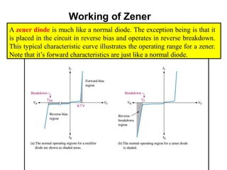
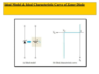
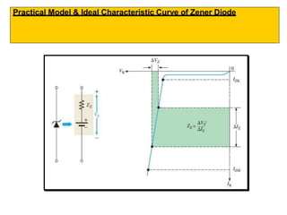
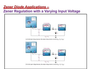
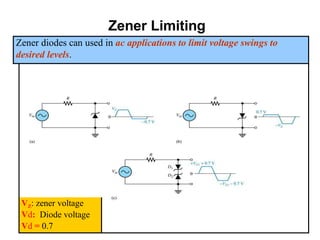
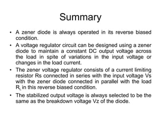
Zener diodes are designed to operate in reverse breakdown. Two types of reverse breakdown
in a zener diode are avalanche and zener. The avalanche break down occurs in both rectifier
and zener diodes at a sufficiently high reverse voltage. Zener breakdown occurs in a zener
diode at low reverse voltages.
A zener diode is heavily doped to reduced the breakdown voltage. This
causes a very thin depletion region.
The zener diodes breakdown characteristics are determined by the doping
process
Zeners are commercially available with voltage breakdowns of 1.8 V to 200
V.
Working of Zener
A zener diode is much like a normal diode. The exception being is that it
is placed in the circuit in reverse bias and operates in reverse breakdown.
This typical characteristic curve illustrates the operating range for a zener.
Note that it’s forward characteristics are just like a normal diode.
Breakdown Characteristics
Figure shows the reverse portion of a zener diode’s characteristic curve.
As the reverse voltage (VR) is increased, the reverse current (IR)
remains extremely small up to the “knee” of the curve. The reverse
current is also called the zener current, IZ. At this point, the breakdown
effect begins; the internal zener resistance, also called zener impedance
(ZZ), begins to decrease as reverse current increases rapidly.
ZENER BREAKDOWN
• Zener and avalanche effects are responsible
for such a dramatic increase in the value of
current at the breakdown voltage.
• If the impurity concentration is very high, then
the width of depletion region is very less.
Less width of depletion region will cause high
intensity of electric field to develop in the
depletion region at low voltages.
• Lets take an example to understand things
clearly.
• Let say the width of depletion region is
200 Å (very small). If a reverse bias
voltage of just 4 V is applied to the diode,
then the electric field intensity in the
depletion region will be
4 = 2 x 10⁸ V/m
200 x 10-10
.
• Avoltage of 4 V is responsible to generate an
electric field intensity of 2 x 10⁸ V/m (very high
intensity).
• This electric field is sufficient to rupture the bonds
and separate the valence electrons from their
respective nuclei.
Large number of electrons gets separated from
their atoms, resulting in sudden increase in the
value of reverse current.
This explanation was given by scientist C. E.
•
•
Zener. Such diodes are called Zener diodes.
• Zener effect predominates in diodes whose
breakdown voltage is below 6 V.
AVALANCHE BEAKDOWN
• Zener effect predominates on diodes whose
breakdown voltage is less. The breakdown
voltage can be obtained at a large value by reducing
the concentration of impurity atom.
• We know that very little amount of current flows in
the reverse biased diode. This current is due to the
flow of minority charge carriers i.e., electrons in the
p type semiconductor and holes in the n type
semiconductor.
The width of depletion
impurity concentration is le.
• region is large when the
ss.
• When a reverse bias voltage is applied across the
terminals of the diode, the electrons from the p type
material and holes from the n-type materials
accelerates through the depletion region.
• This results in collision of intrinsic particles
(electrons and holes) with the bound electrons in the
depletion region. With the increase in reverse bias
voltage the acceleration of electrons and holes also
increases.
Now the intrinsic particles collides with bound
electrons with enough energy to break its covalent
bond and create an electron-hole pair. This is shown
•
Avalanche Breakdown
Mechanism
.
• The collision of electrons with the atom creates an
electron-hole pair.
• This newly created electron also gets accelerated
due to electric field and breaks many more
covalent bond to further create more electron-hole
pair.
This process keeps on repeating and it is
called carrier multiplication.
The newly created electrons and holes contribute
to the rise in reverse current.
The process of carrier multiplication occurs very
quickly and in very large numbers that there is
•
•
•
apparently an avalanche of charge
called
carriers.
avalancheThus the breakdown is
breakdown.
DIFFERENCE BETWEEN ZENER
AND AVALANCHE BREAKDOWN
Zener Breakdown
1.This occurs at junctions which being
heavily doped have narrow depletion
layers
2. This breakdown voltage sets a
very strong electric field across
this narrow layer.
3.Here electric field is very strong
to rupture the covalent bonds
thereby generating electron-hole
pairs. So even a small increase in
reverse voltage is capable of producing
Large number of current carriers.
4.Zener diode exhibits negative temp:
coefficient. Ie. breakdown voltage
decreases as temperature increases.
Avalanche breakdown
1.This occurs at junctions which
being lightly doped have wide depletion layers.
2.Here electric field is not strong
enough to produce Zener breakdown.
3.Here minority carriers collide with semi
conductor atoms in the depletion region, which
breaks the covalent bonds and electron-hole
pairs are generated. Newly generated charge
carriers are accelerated by the electric field
which results in more collision and generates
avalanche of charge carriers. This results in
avalanche breakdown.
4.Avalanche diodes exhibits positive temp:
coefficient. i.e breakdown voltage increases
with increase in temperature.
Ideal Model & Ideal Characteristic Curve of Zener Diode
Practical Model & Ideal Characteristic Curve of Zener Diode
Zener Diode Applications –
Zener Regulation with a Varying Input Voltage
Zener Limiting
Zener diodes can used in ac applications to limit voltage swings to
desired levels.
VZ: zener voltage
Vd: Diode voltage
Vd = 0.7
A zener diode exhibits a certain change in Vz for a certain
change in lz on a portion of the linear characteristic curve
between IZK and IZM as illustrated in Figure.
impedance?
What is the zener
Example
• A 5.0V stabilised power supply is
required
a 12V DC
source.
to be produced
supply
from
inputpower
The maximum power rating Pz of
the zener diode is 2W.
Using the zener regulator circuit
calculate:
a) The maximum current flowing
through the
value
zener diode.
of the seriesb) The
resistor, Rs
c)The
resistor
across
d) The
load current IL if a load
of 1kΩ is connected
diode.
current Is
the
total
Zener
supply
(a)
(b)
(c)
(d)
Summary
• A zener diode is always operated in its reverse biased
condition.
A voltage regulator circuit can be designed using a zener
diode to maintain a constant DC output voltage across
the load in spite of variations in the input voltage or
changes in the load current.
The zener voltage regulator consists of a current limiting
resistor Rs connected in series with the input voltage Vs
with the zener diode connected in parallel with the load
RL in this reverse biased condition.
The stabilized output voltage is always selected to be the
same as the breakdown voltage Vz of the diode.
•
•
•

Zener Diodes

  • 1.
    Zener Diode Dr. RaviShankar Mishra
  • 2.
    Introduction The zener diodeis a silicon pn junction devices that differs from rectifier diodes because it is designed for operation in the reverse-breakdown region. The breakdown voltage of a zener diode is set by carefully controlling the level during manufacture. The basic function of zener diode is to maintain a specific voltage across it’s terminals within given limits of line or load change. Typically it is used for providing a stable reference voltage for use in power supplies and other equipment.
  • 3.
    Construction of Zener Zenerdiodes are designed to operate in reverse breakdown. Two types of reverse breakdown in a zener diode are avalanche and zener. The avalanche break down occurs in both rectifier and zener diodes at a sufficiently high reverse voltage. Zener breakdown occurs in a zener diode at low reverse voltages. A zener diode is heavily doped to reduced the breakdown voltage. This causes a very thin depletion region. The zener diodes breakdown characteristics are determined by the doping process Zeners are commercially available with voltage breakdowns of 1.8 V to 200 V.
  • 4.
    Working of Zener Azener diode is much like a normal diode. The exception being is that it is placed in the circuit in reverse bias and operates in reverse breakdown. This typical characteristic curve illustrates the operating range for a zener. Note that it’s forward characteristics are just like a normal diode.
  • 5.
    Breakdown Characteristics Figure showsthe reverse portion of a zener diode’s characteristic curve. As the reverse voltage (VR) is increased, the reverse current (IR) remains extremely small up to the “knee” of the curve. The reverse current is also called the zener current, IZ. At this point, the breakdown effect begins; the internal zener resistance, also called zener impedance (ZZ), begins to decrease as reverse current increases rapidly.
  • 6.
    ZENER BREAKDOWN • Zenerand avalanche effects are responsible for such a dramatic increase in the value of current at the breakdown voltage. • If the impurity concentration is very high, then the width of depletion region is very less. Less width of depletion region will cause high intensity of electric field to develop in the depletion region at low voltages.
  • 7.
    • Lets takean example to understand things clearly. • Let say the width of depletion region is 200 Å (very small). If a reverse bias voltage of just 4 V is applied to the diode, then the electric field intensity in the depletion region will be 4 = 2 x 10⁸ V/m 200 x 10-10
  • 8.
    . • Avoltage of4 V is responsible to generate an electric field intensity of 2 x 10⁸ V/m (very high intensity). • This electric field is sufficient to rupture the bonds and separate the valence electrons from their respective nuclei. Large number of electrons gets separated from their atoms, resulting in sudden increase in the value of reverse current. This explanation was given by scientist C. E. • • Zener. Such diodes are called Zener diodes. • Zener effect predominates in diodes whose breakdown voltage is below 6 V.
  • 9.
    AVALANCHE BEAKDOWN • Zenereffect predominates on diodes whose breakdown voltage is less. The breakdown voltage can be obtained at a large value by reducing the concentration of impurity atom. • We know that very little amount of current flows in the reverse biased diode. This current is due to the flow of minority charge carriers i.e., electrons in the p type semiconductor and holes in the n type semiconductor.
  • 10.
    The width ofdepletion impurity concentration is le. • region is large when the ss. • When a reverse bias voltage is applied across the terminals of the diode, the electrons from the p type material and holes from the n-type materials accelerates through the depletion region. • This results in collision of intrinsic particles (electrons and holes) with the bound electrons in the depletion region. With the increase in reverse bias voltage the acceleration of electrons and holes also increases. Now the intrinsic particles collides with bound electrons with enough energy to break its covalent bond and create an electron-hole pair. This is shown •
  • 11.
  • 12.
    . • The collisionof electrons with the atom creates an electron-hole pair. • This newly created electron also gets accelerated due to electric field and breaks many more covalent bond to further create more electron-hole pair. This process keeps on repeating and it is called carrier multiplication. The newly created electrons and holes contribute to the rise in reverse current. The process of carrier multiplication occurs very quickly and in very large numbers that there is • • • apparently an avalanche of charge called carriers. avalancheThus the breakdown is breakdown.
  • 13.
    DIFFERENCE BETWEEN ZENER ANDAVALANCHE BREAKDOWN Zener Breakdown 1.This occurs at junctions which being heavily doped have narrow depletion layers 2. This breakdown voltage sets a very strong electric field across this narrow layer. 3.Here electric field is very strong to rupture the covalent bonds thereby generating electron-hole pairs. So even a small increase in reverse voltage is capable of producing Large number of current carriers. 4.Zener diode exhibits negative temp: coefficient. Ie. breakdown voltage decreases as temperature increases. Avalanche breakdown 1.This occurs at junctions which being lightly doped have wide depletion layers. 2.Here electric field is not strong enough to produce Zener breakdown. 3.Here minority carriers collide with semi conductor atoms in the depletion region, which breaks the covalent bonds and electron-hole pairs are generated. Newly generated charge carriers are accelerated by the electric field which results in more collision and generates avalanche of charge carriers. This results in avalanche breakdown. 4.Avalanche diodes exhibits positive temp: coefficient. i.e breakdown voltage increases with increase in temperature.
  • 15.
    Ideal Model &Ideal Characteristic Curve of Zener Diode
  • 16.
    Practical Model &Ideal Characteristic Curve of Zener Diode
  • 17.
    Zener Diode Applications– Zener Regulation with a Varying Input Voltage
  • 18.
    Zener Limiting Zener diodescan used in ac applications to limit voltage swings to desired levels. VZ: zener voltage Vd: Diode voltage Vd = 0.7
  • 19.
    A zener diodeexhibits a certain change in Vz for a certain change in lz on a portion of the linear characteristic curve between IZK and IZM as illustrated in Figure. impedance? What is the zener
  • 20.
    Example • A 5.0Vstabilised power supply is required a 12V DC source. to be produced supply from inputpower The maximum power rating Pz of the zener diode is 2W. Using the zener regulator circuit calculate: a) The maximum current flowing through the value zener diode. of the seriesb) The resistor, Rs c)The resistor across d) The load current IL if a load of 1kΩ is connected diode. current Is the total Zener supply
  • 21.
  • 22.
    Summary • A zenerdiode is always operated in its reverse biased condition. A voltage regulator circuit can be designed using a zener diode to maintain a constant DC output voltage across the load in spite of variations in the input voltage or changes in the load current. The zener voltage regulator consists of a current limiting resistor Rs connected in series with the input voltage Vs with the zener diode connected in parallel with the load RL in this reverse biased condition. The stabilized output voltage is always selected to be the same as the breakdown voltage Vz of the diode. • • •