SlideShare a Scribd company logo
SUB : ELECTRONICS DEVICES & CIRCUITS (2131006) 
Topics : 
The Unbiased Diode, Forward Bias, Reverse Bias, Breakdown, Energy Levels, The energy 
Hill, The Barrier Potential and Temperature , Reverse-Biased Diode 
Created by: 
Meghwal Dinesh S. 130140111041 
Mistry Keyur R. 130140111043 
Nakrani Pratik R. 130140111046
The Unbiased Diode 
What is Diode :- A semiconductor device with two 
terminals, typically allowing the flow of 
current in one direction only. 
What is Unbiased Diode :- when we do not apply any 
source of energy or electricity than a 
diode is said to be unbiased diode.
The Unbiased Diode 
 FORMATION OF P-N JUNCTION 
p type 
semiconductor 
n type 
semiconductor 
Anode 
Cathode 
Junction 
P side is called as N type is called as 
Holes 
Electrones 
Majority 
Minority 
Minority 
Majority 
Diffusion is same
Forward bias 
 If p region is connected to the positive terminal of external dc source & n region is 
connected to negative terminal of dc source is said to be forward biasing. 
If If 
Forward biasing of a diode Symbolic Representation
Operation of a Forward biased Diode 
 
- 
- 
- 
- 
- 
+ 
+ 
+ 
+ 
+ 
+ 
+ 
- 
- 
The holes Converting into 
the negative ions into 
neutral atomes 
p n 
R 
Current 
limiting 
resister 
V 
Due to negative terminal of external 
souce connected to n-region so 
electrons are pushed towards p-side 
Due to Positive terminal of external souce 
connected to p-region so holes are 
pushed towards n-side 
The Electrones Converting 
into the Positive ions into 
neutral atomes Due to this The 
width of deplation 
region will reduce 
Due to reduction in 
the depletion region 
width the barrier also 
reduced. 
Hence a large number 
of electrons & holes can 
cross the junction under 
the influence of 
externally connected 
DC voltage 
As we can say that the flow of electrons is current so that the current produce 
in this position said to be forward Current
Reverse bias 
 If p region is connected to the negative terminal of external dc source & n region is 
connected to Positive terminal of dc source is said to be reverse biasing. 
Ir Ir 
Reverse biasing of a diode Symbolic Representation
Operation of a Reverse biased Diode 
 
- 
- 
- 
- 
- 
+ 
+ 
+ 
+ 
+ 
The process of widening is not take place at longer time due to 
there is no steady flow of current from n-side to p-side 
+ 
+ 
- 
- 
p n 
R Current 
limiting 
resister 
Holes in P region are attracted V 
towards negative terminal of 
supply 
Electrones in n region are 
attracted towards positive 
terminal of supply. 
Due to this The width 
of deplation region will 
incresases 
Due to increases 
in the depletion region 
width the barrier also 
increases. 
Minority carrier in p-region 
attracted 
towards positive of 
supply. 
- 
- 
- 
- 
- 
+ 
+ 
+ 
+ 
+ 
So that few electrons are flow so the current is also tiny that current states at this position 
said to be reverse saturation current due to minority carrier
Breakdown 
The reverse saturation current flowing in reverse biased diode is 
dependent only on temperature & 
independent on reverse applied voltage externally. 
The breakdown in reverse biased diode can take place due to following effects. 
Avalache 
effect 
Zener 
effect 
B 
R 
E 
A 
K 
D 
O 
W 
N
Breakdown due to Avalache effect 
Due to large voltage 
velocity of minority 
carriers will increase 
to great exent 
Therefore Kinetic 
energy also increses 
While traveling 
minority carriers will 
collide with stable 
atomes & import 
some of kinetic 
energy To the 
valance electrons 
present in co-valent 
band 
Due to this 
additional energy 
these electones will 
break the covalent 
bonds &jump into 
the conduction 
band to free for 
conduction. 
Now this free 
electones will be 
accelerated &they 
knockout some 
more valance 
electrons by means 
collisions. 
THIS “CHAIN 
REACTION” IS 
CALLED as 
“AVALANCHE 
EFFECT”
Break down due to Zener effect 
Due to heavy doping of 
p & n side of the diode 
the deplation region is 
narrow in reverse biased 
condition. 
Therefore electrical field 
which is the voltage per 
unit distance is very 
intense across the 
deplation region 
This intense electric field 
can pull some of 
valence electrons by 
breaking the covalent 
bonds these electrons 
than become free 
electrons. 
The large number of 
such electrons can 
constitute through 
diode this is called as 
the breakdown due to 
zener effect
Energy Levals 
 Each electrons orbit has an energy leval associated with it. The electrons in the inner orbits are 
more closely bound to the nucleus to the nucleus and posses less energy. 
 As we move towards the valance shell, the bliding force between nucleus & electrons reduces 
and the electrons reduces & elctrones posses higher energy. 
Shell 1 
Lowest energy 
Energy leval increses as we move 
away from the nucleus 
Valance orbit has 
highest energy leval
Energy Bands 
First band 
Formed by cluster 
of energy leval in 
first shell 
Valence 
band 
Corresponds to 
valance electrons 
present in different 
atomes of 
materials 
Enrgy associated is 
second highest. 
Conduction 
band 
The electrons in 
conduction band 
are the free 
electrons. 
Enrgy associated is 
highest. 
Concept of forbidden gap: 
• Forbidden gap is energy gap that separates the conduction band & Valence bands. 
• For any material the forbidden gap may be large, small , or even nonexistent. The materials 
are classified as conductor , insulator, semiconductors based on relative widths of forbidden 
gap.
 
Energy Hill 
Energy 
Conduction band 
Valence band 
The Valence & 
Conduction bands 
are slightly lower 
energy levals 
This is Due to difference 
in the atomic 
characteristics of the 
pentavalent(n-type) & 
Trivalent(p-tpye) impurity 
atomes 
Minority 
carriers(electrons) 
Majority 
carriers(Holes) 
Majority 
carriers(electrons) 
Minority 
carriers(Holes) 
A p-region n-region K
Barrier Potential & Temperature 
 Inernal temperature of p-n junction is known as the junction temperature 
 Whereas the air surrounding the device is called as ambient temprerature 
For conducting 
Diode 
Junction Temp. > Ambient Temp. 
Barrier Potential 1 
junction temperature 
So that Due to Incresed Temp. barrier potential decreases more electrons & hole 
pair produced . These will diffuse into deplation region to narrow it down. 
The barrier potential of a silicon diode decreases at 2 mV per degree Celsius rise in 
junction temperature. 
-2mV/◦ 퐶 = 
Δ퐕 
Δ퐓
Circuit Courtesy : Circuit Maker 
Platformed by :- Microsoft office 2013

More Related Content

What's hot

Band theory
Band theoryBand theory
Band theory
RAHEELA Khan
 
waveguides-ppt
waveguides-pptwaveguides-ppt
waveguides-ppt
ATTO RATHORE
 
Semiconductor diode
Semiconductor diodeSemiconductor diode
Semiconductor diode
RAMPRAKASHT1
 
Pn junction diode
Pn junction diodePn junction diode
Pn junction diode
Poojith Chowdhary
 
Transistor biasing
Transistor biasing Transistor biasing
Transistor biasing
Anisur Rahman
 
Diode ,its types & its Application
Diode ,its types & its ApplicationDiode ,its types & its Application
Diode ,its types & its Application
SUFYAN SATTAR
 
Schottky diode working and applications
Schottky diode working and applicationsSchottky diode working and applications
Schottky diode working and applications
elprocus
 
Pashen's law
Pashen's lawPashen's law
Pashen's law
mohannad hameed
 
Ferroelectric and piezoelectric materials
Ferroelectric and piezoelectric materialsFerroelectric and piezoelectric materials
Ferroelectric and piezoelectric materials
Zaahir Salam
 
Magnetic materials
Magnetic materialsMagnetic materials
Magnetic materials
Nilay Patel
 
Band theory of solid
Band theory of solidBand theory of solid
Band theory of solid
Keyur Patel
 
PN JUNCTION
PN JUNCTION PN JUNCTION
PN JUNCTION
Mehedi Hasan
 
Metal Semi-Conductor Junctions
Metal Semi-Conductor JunctionsMetal Semi-Conductor Junctions
Metal Semi-Conductor Junctions
Agha Muqaddas Ali Khan
 
Chapter5 carrier transport phenomena
Chapter5 carrier transport phenomenaChapter5 carrier transport phenomena
Chapter5 carrier transport phenomena
K. M.
 
MOSFETs
MOSFETsMOSFETs
MOSFETs
A B Shinde
 
P n junction characteristics
P n junction characteristicsP n junction characteristics
P n junction characteristics
Ashvani Shukla
 
Filter circuits slide_share
Filter circuits slide_shareFilter circuits slide_share
Filter circuits slide_share
SMITHAS35
 
Basic of semiconductors and optical properties
Basic of semiconductors and optical propertiesBasic of semiconductors and optical properties
Basic of semiconductors and optical properties
Kamran Ansari
 

What's hot (20)

Band theory
Band theoryBand theory
Band theory
 
waveguides-ppt
waveguides-pptwaveguides-ppt
waveguides-ppt
 
Semiconductor diode
Semiconductor diodeSemiconductor diode
Semiconductor diode
 
domain theroy
domain theroydomain theroy
domain theroy
 
Pn junction diode
Pn junction diodePn junction diode
Pn junction diode
 
Semiconductor diode
Semiconductor diodeSemiconductor diode
Semiconductor diode
 
Transistor biasing
Transistor biasing Transistor biasing
Transistor biasing
 
Diode ,its types & its Application
Diode ,its types & its ApplicationDiode ,its types & its Application
Diode ,its types & its Application
 
Schottky diode working and applications
Schottky diode working and applicationsSchottky diode working and applications
Schottky diode working and applications
 
Pashen's law
Pashen's lawPashen's law
Pashen's law
 
Ferroelectric and piezoelectric materials
Ferroelectric and piezoelectric materialsFerroelectric and piezoelectric materials
Ferroelectric and piezoelectric materials
 
Magnetic materials
Magnetic materialsMagnetic materials
Magnetic materials
 
Band theory of solid
Band theory of solidBand theory of solid
Band theory of solid
 
PN JUNCTION
PN JUNCTION PN JUNCTION
PN JUNCTION
 
Metal Semi-Conductor Junctions
Metal Semi-Conductor JunctionsMetal Semi-Conductor Junctions
Metal Semi-Conductor Junctions
 
Chapter5 carrier transport phenomena
Chapter5 carrier transport phenomenaChapter5 carrier transport phenomena
Chapter5 carrier transport phenomena
 
MOSFETs
MOSFETsMOSFETs
MOSFETs
 
P n junction characteristics
P n junction characteristicsP n junction characteristics
P n junction characteristics
 
Filter circuits slide_share
Filter circuits slide_shareFilter circuits slide_share
Filter circuits slide_share
 
Basic of semiconductors and optical properties
Basic of semiconductors and optical propertiesBasic of semiconductors and optical properties
Basic of semiconductors and optical properties
 

Viewers also liked

Pn junction diodes (presentation)
Pn junction diodes (presentation)Pn junction diodes (presentation)
Pn junction diodes (presentation)
Alan Bullard
 
Forward and reverse genetics
Forward and reverse geneticsForward and reverse genetics
Forward and reverse genetics
Sachin Ekatpure
 
Diode
DiodeDiode
Diode
musaed119
 
Diodes
DiodesDiodes
Diodes
callr
 
Topic 3 pn_junction_and_diode
Topic 3 pn_junction_and_diodeTopic 3 pn_junction_and_diode
Topic 3 pn_junction_and_diode
Gabriel O'Brien
 
Diodes
DiodesDiodes
Diodes
Soujanya Roy
 
Pn junction diode characteristics Lab expriment
Pn junction diode characteristics Lab exprimentPn junction diode characteristics Lab expriment
Pn junction diode characteristics Lab expriment
dhanajeyan dhanaj
 
Rectifier
RectifierRectifier
Rectifier
zakidaud
 
Presentation on half and full wave ractifier.ppt
Presentation on half and full wave ractifier.pptPresentation on half and full wave ractifier.ppt
Presentation on half and full wave ractifier.ppt
Kawsar Ahmed
 
Basic electronics and electrical first year engineering
Basic electronics and electrical first year engineeringBasic electronics and electrical first year engineering
Basic electronics and electrical first year engineeringron181295
 
statistical error, enquiry, census vs. sample
statistical error, enquiry, census vs. samplestatistical error, enquiry, census vs. sample
statistical error, enquiry, census vs. sampleHina Varshney
 
P-N junction
P-N junction P-N junction
P-N junction
Ashvani Shukla
 
Basic electronics Darya
Basic electronics  DaryaBasic electronics  Darya
Basic electronics Darya
Darya khan
 
FURTHER RESULTS ON THE DIRAC DELTA APPROXIMATION AND THE MOMENT GENERATING FU...
FURTHER RESULTS ON THE DIRAC DELTA APPROXIMATION AND THE MOMENT GENERATING FU...FURTHER RESULTS ON THE DIRAC DELTA APPROXIMATION AND THE MOMENT GENERATING FU...
FURTHER RESULTS ON THE DIRAC DELTA APPROXIMATION AND THE MOMENT GENERATING FU...
IJCNC
 
1.1.3 forward bias and reverse bias
1.1.3 forward bias and reverse bias1.1.3 forward bias and reverse bias
1.1.3 forward bias and reverse bias
Learn By Watch
 
signal and system Dirac delta functions (1)
signal and system Dirac delta functions (1)signal and system Dirac delta functions (1)
signal and system Dirac delta functions (1)
iqbal ahmad
 
1.1. El Diodo Ideal
1.1. El Diodo Ideal1.1. El Diodo Ideal
1.1. El Diodo Ideal
Othoniel Hernandez Ovando
 

Viewers also liked (20)

Pn junction diodes (presentation)
Pn junction diodes (presentation)Pn junction diodes (presentation)
Pn junction diodes (presentation)
 
Semi conductor diode
Semi conductor diodeSemi conductor diode
Semi conductor diode
 
Forward and reverse genetics
Forward and reverse geneticsForward and reverse genetics
Forward and reverse genetics
 
Diode
DiodeDiode
Diode
 
Diodes
DiodesDiodes
Diodes
 
Topic 3 pn_junction_and_diode
Topic 3 pn_junction_and_diodeTopic 3 pn_junction_and_diode
Topic 3 pn_junction_and_diode
 
Diodes
DiodesDiodes
Diodes
 
Pn junction
Pn junctionPn junction
Pn junction
 
Pn junction diode characteristics Lab expriment
Pn junction diode characteristics Lab exprimentPn junction diode characteristics Lab expriment
Pn junction diode characteristics Lab expriment
 
Rectifier
RectifierRectifier
Rectifier
 
Presentation on half and full wave ractifier.ppt
Presentation on half and full wave ractifier.pptPresentation on half and full wave ractifier.ppt
Presentation on half and full wave ractifier.ppt
 
Basic electronics and electrical first year engineering
Basic electronics and electrical first year engineeringBasic electronics and electrical first year engineering
Basic electronics and electrical first year engineering
 
Semiconductor physics
Semiconductor physicsSemiconductor physics
Semiconductor physics
 
statistical error, enquiry, census vs. sample
statistical error, enquiry, census vs. samplestatistical error, enquiry, census vs. sample
statistical error, enquiry, census vs. sample
 
P-N junction
P-N junction P-N junction
P-N junction
 
Basic electronics Darya
Basic electronics  DaryaBasic electronics  Darya
Basic electronics Darya
 
FURTHER RESULTS ON THE DIRAC DELTA APPROXIMATION AND THE MOMENT GENERATING FU...
FURTHER RESULTS ON THE DIRAC DELTA APPROXIMATION AND THE MOMENT GENERATING FU...FURTHER RESULTS ON THE DIRAC DELTA APPROXIMATION AND THE MOMENT GENERATING FU...
FURTHER RESULTS ON THE DIRAC DELTA APPROXIMATION AND THE MOMENT GENERATING FU...
 
1.1.3 forward bias and reverse bias
1.1.3 forward bias and reverse bias1.1.3 forward bias and reverse bias
1.1.3 forward bias and reverse bias
 
signal and system Dirac delta functions (1)
signal and system Dirac delta functions (1)signal and system Dirac delta functions (1)
signal and system Dirac delta functions (1)
 
1.1. El Diodo Ideal
1.1. El Diodo Ideal1.1. El Diodo Ideal
1.1. El Diodo Ideal
 

Similar to [FULL ANIMATED(Download to view)] Unbiased diode, Forward biased , reverse biased diode,breakdown,energy hills

Semiconductor diodes1
Semiconductor diodes1Semiconductor diodes1
Semiconductor diodes1
Sirat Mahmood
 
B.Tech sem I Engineering Physics U-II Chapter 1-Band theory of solid
B.Tech sem I Engineering Physics U-II Chapter 1-Band theory of solidB.Tech sem I Engineering Physics U-II Chapter 1-Band theory of solid
B.Tech sem I Engineering Physics U-II Chapter 1-Band theory of solid
Abhi Hirpara
 
Semiconductor fundamentals.pptx
Semiconductor fundamentals.pptxSemiconductor fundamentals.pptx
Semiconductor fundamentals.pptx
ssuser593a2d
 
BEEME UNIT IV.ppt
BEEME UNIT IV.pptBEEME UNIT IV.ppt
BEEME UNIT IV.ppt
Karthik Kathan
 
SEMICONDUCTOR (project)
SEMICONDUCTOR (project)SEMICONDUCTOR (project)
SEMICONDUCTOR (project)
SUDHA BHUJEL
 
Class 12 th semiconductor part 3
Class 12 th semiconductor part 3Class 12 th semiconductor part 3
Class 12 th semiconductor part 3
Priyanka Jakhar
 
Electronics Engineering Diode , Transistor ,BJT
Electronics Engineering Diode , Transistor ,BJTElectronics Engineering Diode , Transistor ,BJT
Electronics Engineering Diode , Transistor ,BJT
yadavsuyash008
 
BEEIE UNIT IV PPT.ppt
BEEIE UNIT IV PPT.pptBEEIE UNIT IV PPT.ppt
BEEIE UNIT IV PPT.ppt
DEEBIKAR2
 
Analog circuits-lab-possible-viva-questions
Analog circuits-lab-possible-viva-questionsAnalog circuits-lab-possible-viva-questions
Analog circuits-lab-possible-viva-questions
padmajasiva
 
BEEE.pptx
BEEE.pptxBEEE.pptx
BEEE.pptx
AayushBhure
 
Electronic Devices and Circuits by Dr. R.Prakash Rao
Electronic Devices and Circuits by Dr. R.Prakash RaoElectronic Devices and Circuits by Dr. R.Prakash Rao
Electronic Devices and Circuits by Dr. R.Prakash Rao
rachurivlsi
 
Semiconductors
SemiconductorsSemiconductors
Semiconductors
HarshitParkar6677
 
EC 8353 EDC
EC 8353 EDCEC 8353 EDC
EC 8353 EDC
rmkceteee
 
B.tech sem i engineering physics u ii chapter 1-band theory of solid
B.tech sem i engineering physics u ii chapter 1-band theory of solidB.tech sem i engineering physics u ii chapter 1-band theory of solid
B.tech sem i engineering physics u ii chapter 1-band theory of solid
Rai University
 
New.pdf
New.pdfNew.pdf
UNIT 3 Analog Electronics.pptx
UNIT 3 Analog Electronics.pptxUNIT 3 Analog Electronics.pptx
UNIT 3 Analog Electronics.pptx
DHARUNESHBOOPATHY
 
Diode
DiodeDiode
Semiconductors N. m.Aher
Semiconductors N. m.AherSemiconductors N. m.Aher
Semiconductors N. m.Aher
NandalalAher1
 
UNIT 1- Semiconductor diodes (3).pptx
UNIT 1- Semiconductor diodes (3).pptxUNIT 1- Semiconductor diodes (3).pptx
UNIT 1- Semiconductor diodes (3).pptx
nakkabava24
 

Similar to [FULL ANIMATED(Download to view)] Unbiased diode, Forward biased , reverse biased diode,breakdown,energy hills (20)

Theory of solids
Theory of solidsTheory of solids
Theory of solids
 
Semiconductor diodes1
Semiconductor diodes1Semiconductor diodes1
Semiconductor diodes1
 
B.Tech sem I Engineering Physics U-II Chapter 1-Band theory of solid
B.Tech sem I Engineering Physics U-II Chapter 1-Band theory of solidB.Tech sem I Engineering Physics U-II Chapter 1-Band theory of solid
B.Tech sem I Engineering Physics U-II Chapter 1-Band theory of solid
 
Semiconductor fundamentals.pptx
Semiconductor fundamentals.pptxSemiconductor fundamentals.pptx
Semiconductor fundamentals.pptx
 
BEEME UNIT IV.ppt
BEEME UNIT IV.pptBEEME UNIT IV.ppt
BEEME UNIT IV.ppt
 
SEMICONDUCTOR (project)
SEMICONDUCTOR (project)SEMICONDUCTOR (project)
SEMICONDUCTOR (project)
 
Class 12 th semiconductor part 3
Class 12 th semiconductor part 3Class 12 th semiconductor part 3
Class 12 th semiconductor part 3
 
Electronics Engineering Diode , Transistor ,BJT
Electronics Engineering Diode , Transistor ,BJTElectronics Engineering Diode , Transistor ,BJT
Electronics Engineering Diode , Transistor ,BJT
 
BEEIE UNIT IV PPT.ppt
BEEIE UNIT IV PPT.pptBEEIE UNIT IV PPT.ppt
BEEIE UNIT IV PPT.ppt
 
Analog circuits-lab-possible-viva-questions
Analog circuits-lab-possible-viva-questionsAnalog circuits-lab-possible-viva-questions
Analog circuits-lab-possible-viva-questions
 
BEEE.pptx
BEEE.pptxBEEE.pptx
BEEE.pptx
 
Electronic Devices and Circuits by Dr. R.Prakash Rao
Electronic Devices and Circuits by Dr. R.Prakash RaoElectronic Devices and Circuits by Dr. R.Prakash Rao
Electronic Devices and Circuits by Dr. R.Prakash Rao
 
Semiconductors
SemiconductorsSemiconductors
Semiconductors
 
EC 8353 EDC
EC 8353 EDCEC 8353 EDC
EC 8353 EDC
 
B.tech sem i engineering physics u ii chapter 1-band theory of solid
B.tech sem i engineering physics u ii chapter 1-band theory of solidB.tech sem i engineering physics u ii chapter 1-band theory of solid
B.tech sem i engineering physics u ii chapter 1-band theory of solid
 
New.pdf
New.pdfNew.pdf
New.pdf
 
UNIT 3 Analog Electronics.pptx
UNIT 3 Analog Electronics.pptxUNIT 3 Analog Electronics.pptx
UNIT 3 Analog Electronics.pptx
 
Diode
DiodeDiode
Diode
 
Semiconductors N. m.Aher
Semiconductors N. m.AherSemiconductors N. m.Aher
Semiconductors N. m.Aher
 
UNIT 1- Semiconductor diodes (3).pptx
UNIT 1- Semiconductor diodes (3).pptxUNIT 1- Semiconductor diodes (3).pptx
UNIT 1- Semiconductor diodes (3).pptx
 

Recently uploaded

Building Electrical System Design & Installation
Building Electrical System Design & InstallationBuilding Electrical System Design & Installation
Building Electrical System Design & Installation
symbo111
 
Governing Equations for Fundamental Aerodynamics_Anderson2010.pdf
Governing Equations for Fundamental Aerodynamics_Anderson2010.pdfGoverning Equations for Fundamental Aerodynamics_Anderson2010.pdf
Governing Equations for Fundamental Aerodynamics_Anderson2010.pdf
WENKENLI1
 
Gen AI Study Jams _ For the GDSC Leads in India.pdf
Gen AI Study Jams _ For the GDSC Leads in India.pdfGen AI Study Jams _ For the GDSC Leads in India.pdf
Gen AI Study Jams _ For the GDSC Leads in India.pdf
gdsczhcet
 
CME397 Surface Engineering- Professional Elective
CME397 Surface Engineering- Professional ElectiveCME397 Surface Engineering- Professional Elective
CME397 Surface Engineering- Professional Elective
karthi keyan
 
Planning Of Procurement o different goods and services
Planning Of Procurement o different goods and servicesPlanning Of Procurement o different goods and services
Planning Of Procurement o different goods and services
JoytuBarua2
 
Final project report on grocery store management system..pdf
Final project report on grocery store management system..pdfFinal project report on grocery store management system..pdf
Final project report on grocery store management system..pdf
Kamal Acharya
 
Hybrid optimization of pumped hydro system and solar- Engr. Abdul-Azeez.pdf
Hybrid optimization of pumped hydro system and solar- Engr. Abdul-Azeez.pdfHybrid optimization of pumped hydro system and solar- Engr. Abdul-Azeez.pdf
Hybrid optimization of pumped hydro system and solar- Engr. Abdul-Azeez.pdf
fxintegritypublishin
 
Water Industry Process Automation and Control Monthly - May 2024.pdf
Water Industry Process Automation and Control Monthly - May 2024.pdfWater Industry Process Automation and Control Monthly - May 2024.pdf
Water Industry Process Automation and Control Monthly - May 2024.pdf
Water Industry Process Automation & Control
 
Basic Industrial Engineering terms for apparel
Basic Industrial Engineering terms for apparelBasic Industrial Engineering terms for apparel
Basic Industrial Engineering terms for apparel
top1002
 
Heap Sort (SS).ppt FOR ENGINEERING GRADUATES, BCA, MCA, MTECH, BSC STUDENTS
Heap Sort (SS).ppt FOR ENGINEERING GRADUATES, BCA, MCA, MTECH, BSC STUDENTSHeap Sort (SS).ppt FOR ENGINEERING GRADUATES, BCA, MCA, MTECH, BSC STUDENTS
Heap Sort (SS).ppt FOR ENGINEERING GRADUATES, BCA, MCA, MTECH, BSC STUDENTS
Soumen Santra
 
Student information management system project report ii.pdf
Student information management system project report ii.pdfStudent information management system project report ii.pdf
Student information management system project report ii.pdf
Kamal Acharya
 
Immunizing Image Classifiers Against Localized Adversary Attacks
Immunizing Image Classifiers Against Localized Adversary AttacksImmunizing Image Classifiers Against Localized Adversary Attacks
Immunizing Image Classifiers Against Localized Adversary Attacks
gerogepatton
 
Hierarchical Digital Twin of a Naval Power System
Hierarchical Digital Twin of a Naval Power SystemHierarchical Digital Twin of a Naval Power System
Hierarchical Digital Twin of a Naval Power System
Kerry Sado
 
一比一原版(IIT毕业证)伊利诺伊理工大学毕业证成绩单专业办理
一比一原版(IIT毕业证)伊利诺伊理工大学毕业证成绩单专业办理一比一原版(IIT毕业证)伊利诺伊理工大学毕业证成绩单专业办理
一比一原版(IIT毕业证)伊利诺伊理工大学毕业证成绩单专业办理
zwunae
 
Cosmetic shop management system project report.pdf
Cosmetic shop management system project report.pdfCosmetic shop management system project report.pdf
Cosmetic shop management system project report.pdf
Kamal Acharya
 
space technology lecture notes on satellite
space technology lecture notes on satellitespace technology lecture notes on satellite
space technology lecture notes on satellite
ongomchris
 
Fundamentals of Electric Drives and its applications.pptx
Fundamentals of Electric Drives and its applications.pptxFundamentals of Electric Drives and its applications.pptx
Fundamentals of Electric Drives and its applications.pptx
manasideore6
 
在线办理(ANU毕业证书)澳洲国立大学毕业证录取通知书一模一样
在线办理(ANU毕业证书)澳洲国立大学毕业证录取通知书一模一样在线办理(ANU毕业证书)澳洲国立大学毕业证录取通知书一模一样
在线办理(ANU毕业证书)澳洲国立大学毕业证录取通知书一模一样
obonagu
 
weather web application report.pdf
weather web application report.pdfweather web application report.pdf
weather web application report.pdf
Pratik Pawar
 
Tutorial for 16S rRNA Gene Analysis with QIIME2.pdf
Tutorial for 16S rRNA Gene Analysis with QIIME2.pdfTutorial for 16S rRNA Gene Analysis with QIIME2.pdf
Tutorial for 16S rRNA Gene Analysis with QIIME2.pdf
aqil azizi
 

Recently uploaded (20)

Building Electrical System Design & Installation
Building Electrical System Design & InstallationBuilding Electrical System Design & Installation
Building Electrical System Design & Installation
 
Governing Equations for Fundamental Aerodynamics_Anderson2010.pdf
Governing Equations for Fundamental Aerodynamics_Anderson2010.pdfGoverning Equations for Fundamental Aerodynamics_Anderson2010.pdf
Governing Equations for Fundamental Aerodynamics_Anderson2010.pdf
 
Gen AI Study Jams _ For the GDSC Leads in India.pdf
Gen AI Study Jams _ For the GDSC Leads in India.pdfGen AI Study Jams _ For the GDSC Leads in India.pdf
Gen AI Study Jams _ For the GDSC Leads in India.pdf
 
CME397 Surface Engineering- Professional Elective
CME397 Surface Engineering- Professional ElectiveCME397 Surface Engineering- Professional Elective
CME397 Surface Engineering- Professional Elective
 
Planning Of Procurement o different goods and services
Planning Of Procurement o different goods and servicesPlanning Of Procurement o different goods and services
Planning Of Procurement o different goods and services
 
Final project report on grocery store management system..pdf
Final project report on grocery store management system..pdfFinal project report on grocery store management system..pdf
Final project report on grocery store management system..pdf
 
Hybrid optimization of pumped hydro system and solar- Engr. Abdul-Azeez.pdf
Hybrid optimization of pumped hydro system and solar- Engr. Abdul-Azeez.pdfHybrid optimization of pumped hydro system and solar- Engr. Abdul-Azeez.pdf
Hybrid optimization of pumped hydro system and solar- Engr. Abdul-Azeez.pdf
 
Water Industry Process Automation and Control Monthly - May 2024.pdf
Water Industry Process Automation and Control Monthly - May 2024.pdfWater Industry Process Automation and Control Monthly - May 2024.pdf
Water Industry Process Automation and Control Monthly - May 2024.pdf
 
Basic Industrial Engineering terms for apparel
Basic Industrial Engineering terms for apparelBasic Industrial Engineering terms for apparel
Basic Industrial Engineering terms for apparel
 
Heap Sort (SS).ppt FOR ENGINEERING GRADUATES, BCA, MCA, MTECH, BSC STUDENTS
Heap Sort (SS).ppt FOR ENGINEERING GRADUATES, BCA, MCA, MTECH, BSC STUDENTSHeap Sort (SS).ppt FOR ENGINEERING GRADUATES, BCA, MCA, MTECH, BSC STUDENTS
Heap Sort (SS).ppt FOR ENGINEERING GRADUATES, BCA, MCA, MTECH, BSC STUDENTS
 
Student information management system project report ii.pdf
Student information management system project report ii.pdfStudent information management system project report ii.pdf
Student information management system project report ii.pdf
 
Immunizing Image Classifiers Against Localized Adversary Attacks
Immunizing Image Classifiers Against Localized Adversary AttacksImmunizing Image Classifiers Against Localized Adversary Attacks
Immunizing Image Classifiers Against Localized Adversary Attacks
 
Hierarchical Digital Twin of a Naval Power System
Hierarchical Digital Twin of a Naval Power SystemHierarchical Digital Twin of a Naval Power System
Hierarchical Digital Twin of a Naval Power System
 
一比一原版(IIT毕业证)伊利诺伊理工大学毕业证成绩单专业办理
一比一原版(IIT毕业证)伊利诺伊理工大学毕业证成绩单专业办理一比一原版(IIT毕业证)伊利诺伊理工大学毕业证成绩单专业办理
一比一原版(IIT毕业证)伊利诺伊理工大学毕业证成绩单专业办理
 
Cosmetic shop management system project report.pdf
Cosmetic shop management system project report.pdfCosmetic shop management system project report.pdf
Cosmetic shop management system project report.pdf
 
space technology lecture notes on satellite
space technology lecture notes on satellitespace technology lecture notes on satellite
space technology lecture notes on satellite
 
Fundamentals of Electric Drives and its applications.pptx
Fundamentals of Electric Drives and its applications.pptxFundamentals of Electric Drives and its applications.pptx
Fundamentals of Electric Drives and its applications.pptx
 
在线办理(ANU毕业证书)澳洲国立大学毕业证录取通知书一模一样
在线办理(ANU毕业证书)澳洲国立大学毕业证录取通知书一模一样在线办理(ANU毕业证书)澳洲国立大学毕业证录取通知书一模一样
在线办理(ANU毕业证书)澳洲国立大学毕业证录取通知书一模一样
 
weather web application report.pdf
weather web application report.pdfweather web application report.pdf
weather web application report.pdf
 
Tutorial for 16S rRNA Gene Analysis with QIIME2.pdf
Tutorial for 16S rRNA Gene Analysis with QIIME2.pdfTutorial for 16S rRNA Gene Analysis with QIIME2.pdf
Tutorial for 16S rRNA Gene Analysis with QIIME2.pdf
 

[FULL ANIMATED(Download to view)] Unbiased diode, Forward biased , reverse biased diode,breakdown,energy hills

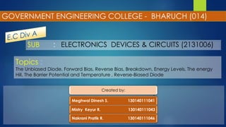
  • 1. SUB : ELECTRONICS DEVICES & CIRCUITS (2131006) Topics : The Unbiased Diode, Forward Bias, Reverse Bias, Breakdown, Energy Levels, The energy Hill, The Barrier Potential and Temperature , Reverse-Biased Diode Created by: Meghwal Dinesh S. 130140111041 Mistry Keyur R. 130140111043 Nakrani Pratik R. 130140111046
  • 2. The Unbiased Diode What is Diode :- A semiconductor device with two terminals, typically allowing the flow of current in one direction only. What is Unbiased Diode :- when we do not apply any source of energy or electricity than a diode is said to be unbiased diode.
  • 3. The Unbiased Diode  FORMATION OF P-N JUNCTION p type semiconductor n type semiconductor Anode Cathode Junction P side is called as N type is called as Holes Electrones Majority Minority Minority Majority Diffusion is same
  • 4. Forward bias  If p region is connected to the positive terminal of external dc source & n region is connected to negative terminal of dc source is said to be forward biasing. If If Forward biasing of a diode Symbolic Representation
  • 5. Operation of a Forward biased Diode  - - - - - + + + + + + + - - The holes Converting into the negative ions into neutral atomes p n R Current limiting resister V Due to negative terminal of external souce connected to n-region so electrons are pushed towards p-side Due to Positive terminal of external souce connected to p-region so holes are pushed towards n-side The Electrones Converting into the Positive ions into neutral atomes Due to this The width of deplation region will reduce Due to reduction in the depletion region width the barrier also reduced. Hence a large number of electrons & holes can cross the junction under the influence of externally connected DC voltage As we can say that the flow of electrons is current so that the current produce in this position said to be forward Current
  • 6. Reverse bias  If p region is connected to the negative terminal of external dc source & n region is connected to Positive terminal of dc source is said to be reverse biasing. Ir Ir Reverse biasing of a diode Symbolic Representation
  • 7. Operation of a Reverse biased Diode  - - - - - + + + + + The process of widening is not take place at longer time due to there is no steady flow of current from n-side to p-side + + - - p n R Current limiting resister Holes in P region are attracted V towards negative terminal of supply Electrones in n region are attracted towards positive terminal of supply. Due to this The width of deplation region will incresases Due to increases in the depletion region width the barrier also increases. Minority carrier in p-region attracted towards positive of supply. - - - - - + + + + + So that few electrons are flow so the current is also tiny that current states at this position said to be reverse saturation current due to minority carrier
  • 8. Breakdown The reverse saturation current flowing in reverse biased diode is dependent only on temperature & independent on reverse applied voltage externally. The breakdown in reverse biased diode can take place due to following effects. Avalache effect Zener effect B R E A K D O W N
  • 9. Breakdown due to Avalache effect Due to large voltage velocity of minority carriers will increase to great exent Therefore Kinetic energy also increses While traveling minority carriers will collide with stable atomes & import some of kinetic energy To the valance electrons present in co-valent band Due to this additional energy these electones will break the covalent bonds &jump into the conduction band to free for conduction. Now this free electones will be accelerated &they knockout some more valance electrons by means collisions. THIS “CHAIN REACTION” IS CALLED as “AVALANCHE EFFECT”
  • 10. Break down due to Zener effect Due to heavy doping of p & n side of the diode the deplation region is narrow in reverse biased condition. Therefore electrical field which is the voltage per unit distance is very intense across the deplation region This intense electric field can pull some of valence electrons by breaking the covalent bonds these electrons than become free electrons. The large number of such electrons can constitute through diode this is called as the breakdown due to zener effect
  • 11. Energy Levals  Each electrons orbit has an energy leval associated with it. The electrons in the inner orbits are more closely bound to the nucleus to the nucleus and posses less energy.  As we move towards the valance shell, the bliding force between nucleus & electrons reduces and the electrons reduces & elctrones posses higher energy. Shell 1 Lowest energy Energy leval increses as we move away from the nucleus Valance orbit has highest energy leval
  • 12. Energy Bands First band Formed by cluster of energy leval in first shell Valence band Corresponds to valance electrons present in different atomes of materials Enrgy associated is second highest. Conduction band The electrons in conduction band are the free electrons. Enrgy associated is highest. Concept of forbidden gap: • Forbidden gap is energy gap that separates the conduction band & Valence bands. • For any material the forbidden gap may be large, small , or even nonexistent. The materials are classified as conductor , insulator, semiconductors based on relative widths of forbidden gap.
  • 13.  Energy Hill Energy Conduction band Valence band The Valence & Conduction bands are slightly lower energy levals This is Due to difference in the atomic characteristics of the pentavalent(n-type) & Trivalent(p-tpye) impurity atomes Minority carriers(electrons) Majority carriers(Holes) Majority carriers(electrons) Minority carriers(Holes) A p-region n-region K
  • 14. Barrier Potential & Temperature  Inernal temperature of p-n junction is known as the junction temperature  Whereas the air surrounding the device is called as ambient temprerature For conducting Diode Junction Temp. > Ambient Temp. Barrier Potential 1 junction temperature So that Due to Incresed Temp. barrier potential decreases more electrons & hole pair produced . These will diffuse into deplation region to narrow it down. The barrier potential of a silicon diode decreases at 2 mV per degree Celsius rise in junction temperature. -2mV/◦ 퐶 = Δ퐕 Δ퐓
  • 15. Circuit Courtesy : Circuit Maker Platformed by :- Microsoft office 2013