Downloaded 347 times


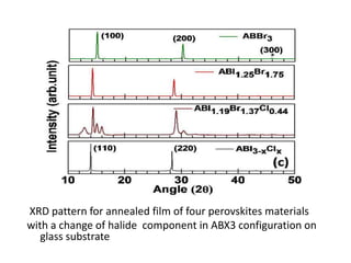


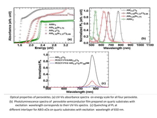


The document explores organometallic halide perovskites used in electroluminescent diodes, discussing their structural and optical properties, and production techniques. It highlights their advantages such as tunable bandgap, high optical absorption, and application in photovoltaics, while cautioning about stability and toxicity issues. Key characterization methods like X-ray diffraction and electronic spectroscopy are presented to analyze material properties and behaviors.


![Presentation1 (1). [163].pptx amit.pptx](https://cdn.slidesharecdn.com/ss_thumbnails/presentation11163-240711044754-e7fd0870-thumbnail.jpg?width=640&height=640&fit=bounds)


