Pentacene-Based Organic Field-Effect Transistors: Analytical Model and Simula...IDES Editor
Organic Field-Effect Transistors, OFETs, attract
much interest recently and their proficiency and hence
applications are being enhanced increasingly. However, only
analytical model of old field-effect transistors, developed for
silicon-based transistors, and their relevant numerical
analyses have been used for such devices, so far. Increasing
precision of such models and numerical methods are essential
now in order to modify OFETs and propose more effective
models and methods. This study pegs at comparing current
analytical model, simulation methods and experiment data
and their fitness with each other. Certainly, four aspects of
results of three abovementioned approaches were examined
comparatively: sub-threshold slope, on-state drain current,
threshold voltage and carrier mobility. We embark to analyze
related experiment data of OFETs made by pentacene, as the
organic material, along with various organic gate insulators
including CyEP, PVP, PMMA, Parylene-C and Polyimide and
then to offer their results, comparatively.
Vapor growth of binary and ternary phosphorusbased semiconductors into TiO2 n...Pawan Kumar
We report successful synthesis of low band gap inorganic polyphosphide and TiO2 heterostructures with
the aid of short-way transport reactions. Binary and ternary polyphosphides (NaP7, SnIP, and (CuI)3P12)
were successfully reacted and deposited into electrochemically fabricated TiO2 nanotubes. Employing
vapor phase reaction deposition, the cavities of 100 mm long TiO2 nanotubes were infiltrated;
approximately 50% of the nanotube arrays were estimated to be infiltrated in the case of NaP7. Intensive
characterization of the hybrid materials with techniques including SEM, FIB, HR-TEM, Raman
spectroscopy, XRD, and XPS proved the successful vapor phase deposition and synthesis of the
substances on and inside the nanotubes. The polyphosphide@TiO2 hybrids exhibited superior water
splitting performance compared to pristine materials and were found to be more active at higher
wavelengths. SnIP@TiO2 emerged to be the most active among the polyphosphide@TiO2 materials. The
improved photocatalytic performance might be due to Fermi level re-alignment and a lower charge
transfer resistance which facilitated better charge separation from inorganic phosphides to TiO2.
Exploiting the potential of 2-((5-(4-(diphenylamino)- phenyl)thiophen-2-yl)me...Akinola Oyedele
A comprehensive experimental study is reported on the optical and electrical characteristics of 2-((5-(4-
(diphenylamino)phenyl)thiophen-2-yl)methylene)malononitrile (DPTMM) when used as molecular donor
in an organic solar cell (OSC) device structure.
Quantum dots for optoelectronic devices - phdassistancePhD Assistance
Nanometre-scale semiconductor chips have been imagined as next-generation technology with high functionality and convergence. Quantum dots, also known as artificial atoms, have special properties owing to their quantum confinement in all three dimensions. Quantum dots have a lot of interest in optoelectronic systems because of their special properties.
For decades, self-assembled nanostructures have been a topic of considerable concern and significance.
Learn More:https://bit.ly/3xJJAiZ
Contact Us:
Website: https://www.phdassistance.com/
UK: +44 7537144372
India No:+91-9176966446
Email: info@phdassistance.com
Recent progress in non platinum counter electrode materials for dye sensitize...Science Padayatchi
Dye-sensitized solar cells (DSSCs) have gained increasing attention
with regard to photovoltaic devices, because of their low
cost and simple fabrication methods; they are mostly investigated
in indoor light-harvesting and portable applications. The
focus has been on three main parameters of photovoltaic devices,
that is, lifetime, and cost effectiveness. A DSSC consists of
four prominent components including a photoanode, a photosensitizer,
a redox electrolyte, and a counter electrode. The
counter electrode is a crucial component, in which triiodide is
reduced to iodide by electrons flowing through the external
circuit. An effective approach to improve the performance of
a counter electrode is to enhance the power conversion efficiency
and to reduce the cost of the device. Platinum-coated
conducting glass electrodes give the best performance, but
their high cost and the scarcity of platinum restricts large-scale
application in DSSCs. This has prompted researchers to develop
low-costing platinum-free electrodes for DSSCs. In this
review, we focus mainly on counter electrode materials for the
electrocatalytic redox reaction for the I¢/I¢
3 electrolyte, and
apart from this, other counter electrode materials for iodinefree
redox electrolytes are discussed. Different counter electrode
materials are highlighted in different categories such as
carbon materials, conducting polymers, oxide and sulfide materials,
transition-metal nitrides and carbides, and composite
materials. The stability of counter electrodes in DSSCs is also
presented.
This document describes research on using p-type transparent conducting oxides (p-TCOs) as protection layers for n-type semiconductor photoanodes used in solar water splitting devices. Specifically, it investigates using nickel cobaltite (NiCo2O4) as the p-TCO layer deposited on n-type silicon (n-Si) and indium phosphide (n-InP) photoanodes. Key findings include:
1) NiCo2O4 functions as both a selective hole contact and corrosion protection layer, allowing for stable water oxidation.
2) A 40nm NiCo2O4 layer provides acceptable corrosion protection and optical transparency for the photoanodes.
3)
Probing electrical energy storage chemistry and physics over broad time and ...Andrew Gelston
This document discusses emerging techniques for characterizing electrical energy storage devices with high spatial and temporal resolution. It describes how neutron scattering, X-ray scattering, electron microscopy, nuclear magnetic resonance, and nonlinear laser techniques can provide insights into chemical and physical phenomena over broad time and length scales. Developing combinations of in situ techniques with both high spatial resolution (down to the atomic scale) and high temporal resolution (down to the femtosecond range) could lead to improvements in battery and capacitor performance and a better understanding of failure mechanisms.
Charge Transport in organic semiconductorsTauqueer Khan
This document summarizes research on synthesizing cadmium telluride (CdTe) nanocrystals directly within a poly(3-hexylthiophene) (P3HT) matrix for use in photovoltaic devices. The in situ growth improves the polymer-nanoparticle interface facilitating efficient charge transfer. Spectral results suggest CdTe forms a charge transfer complex with P3HT via dipole-dipole interaction. Structural studies show CdTe facilitates charge transport pathways between polymer chains. Photovoltaic devices using P3HT-CdTe nanocomposites demonstrated enhanced current density and open circuit voltage compared to P3HT:PCBM devices due to increased energy level offset between donor and
Polymeric carbon nitride-based photocatalysts for photoreforming of biomass d...Pawan Kumar
Photoreforming of biomass to value-added chemicals and fuels is a chemical approach to extract photosynthetically-trapped energy in complex biomolecules which otherwise disintegrate naturally in the environment. Designing precise photocatalytic materials that can selectively break the sturdy, nature-designed biomass with multiplex chemical composition/bonding and inaccessible sites is central to deploying this technology. Polymeric carbon nitride (CN) comprised of a 2D network of condensed heptazine/triazine (C6N7/C3N3) core has shown great promise for photoreforming of biomass derivatives due to intriguing physicochemical and optical properties. This review comprehensively summarizes the state-of-the-art applications of CN-based photocatalysts for the conversion of lignocellulosic biomass derivatives. Various chemical and structural modifications in CN structure such as doping, surface functionalization, hybridization entailing to higher selectivity and conversion have been discussed aiming at providing valuable guidance for future CN-based materials design.
This document discusses X-ray diffraction (XRD) spectroscopy and provides examples of applying XRD principles to characterize different materials. It describes the basic principles of how XRD works using Bragg's law and Miller indices to identify crystal planes. Examples are given for characterizing silver nanoparticles, graphite, graphene oxide, and zinc oxide nanoparticles using XRD, including estimating particle sizes from XRD peak widths and identifying functional groups from infrared spectroscopy. References are also provided for further reading.
Organic field-effect transistors (OFETs) use organic semiconductors like pentacene that can be deposited through low-cost solution processing. OFETs have the potential for applications requiring flexibility and large-area coverage. Pentacene has shown high carrier mobility, with mobilities on par with amorphous silicon in the best OFETs. While progress has been made, understanding charge transport and developing n-type and ambipolar materials remains an area of ongoing research to further improve organic electronics.
This document discusses testing the chemical resistance of PEDOT (poly(3,4-ethylenedioxythiophene)) coated on textile substrates via vapor phase polymerization. Samples were submerged in various organic and inorganic solvents for up to 72 hours. 10% sodium hydroxide most significantly increased electrical resistance over time, removing the PEDOT layer. Tetrahydrofuran removed the PEDOT layer within 24 hours. Weight loss correlated with decreasing conductivity. Scanning electron microscopy images showed PEDOT removal from sodium hydroxide and THF treated samples.
1D Nanomaterials: Design, Synthesis, and Applications in Sodium–Ion BatteriesBilal Qadir
This document reviews 1D nanomaterials and their applications in sodium-ion batteries (SIBs). 1D nanomaterials such as nanofibers, nanotubes, nanorods, and nanowires are promising electrode materials for SIBs due to their uniform structure, oriented ion and electron transport, and ability to tolerate stress changes. The document discusses various synthetic methods for producing 1D nanomaterials, including electrospinning, gas-phase routes, solution-phase routes, and template-assisted methods. It also examines how different morphologies and structural features of 1D nanomaterials can affect electrochemical properties in SIBs. Finally, the document outlines challenges in fabricating 1D nanomaterials and prospects for their future use in
Recent progress in non platinum counter electrode materials for dye sensitize...Science Padayatchi
This document discusses recent progress in developing non-platinum counter electrode materials for dye-sensitized solar cells (DSSCs). It reviews various platinum-free materials that have been studied as alternatives to the traditionally used platinum counter electrodes in DSSCs. These include carbon-based materials like graphene and carbon nanotubes, conducting polymers, metal oxides and sulfides, transition metal nitrides and carbides, and composite materials. The document analyzes the advantages of these materials and their potential to lower the cost of DSSCs while maintaining good performance compared to expensive platinum electrodes.
Vapor Deposition of Semiconducting Phosphorus Allotropes into TiO2 Nanotube A...Pawan Kumar
Recent evidence of exponential environmental degradation will demand a drastic shift in research and development toward exploiting alternative energy resources such as solar energy. Here, we report the successful low-cost and easily accessible synthesis of hybrid semiconductor@TiO2 nanotube photocatalysts. In order to realize its maximum potential in harvesting photons in the visible-light range, TiO2 nanotubes have been loaded with earth-abundant, low-band-gap fibrous red and black phosphorus (P). Scanning electron microscopy– and scanning transmission electron microscopy–energy-dispersive X-ray spectroscopy, X-ray diffraction, Raman spectroscopy, X-ray photoelectron microscopy, and UV–vis measurements have been performed, substantiating the deposition of fibrous red and black P on top and inside the cavities of 100-μm-long electrochemically fabricated nanotubes. The nanotubular …
This document discusses Molybdenum disulfide (MoS2) as a new material for biosensors. MoS2 is a 2D semiconductor with tunable band structure and high carrier mobility. It can be synthesized through mechanical exfoliation, solution methods, and chemical vapor deposition. MoS2 has applications in sensors, memory, photovoltaics due to its direct bandgap and flexibility. Functionalized MoS2 can be used to develop electrode-based and optical biosensors to detect molecules like glucose and dopamine. While MoS2 shows promise for flexible electronics and biosensing, further studies are needed to optimize device performance and compatibility with plastic substrates.
Analysis of Conducting Polymer:Polypyrrole::Part 2Debajyoti Biswas
1. Polypyrrole films doped with different ions exhibit varying levels of crystallinity, thermal stability, and electrical conductivity based on the dopant used. Films doped with camphor sulfonic acid and polyphosphate ions show higher crystallinity levels and better thermal stability compared to films doped with hydrochloric acid or perchlorate ions.
2. The conductivity of polypyrrole increases with decreasing diameter of polypyrrole tubules. Raman spectroscopy indicates that ordering of polymer chains improves at smaller tubule diameters, leading to higher conductivity.
3. Thermogravimetric analysis shows polypyrrole undergoes weight loss in three distinct stages involving loss of dopant and degradation of the
About general characteristics and brief overview about conducting polymers and insights into the various applications of conducting polymers and also general overview about doping and conductivity characteristics
This document describes the fabrication and testing of a high-performance tandem organic solar cell with novel active layers. It utilizes a record-efficiency polymer, PBTI3T, in combination with other polymers like PTB7 and PSBTBT-Si to further enhance efficiency. Absorption spectra of the polymers show offset peaks that minimize spectral overlap when combined in a tandem device. Tandem devices were fabricated with PBTI3T and either PTB7 or PSBTBT-Si as the active layers. Results showed one of the highest open-circuit voltages reported and an overall power conversion efficiency above 6%, demonstrating the potential of tandem organic photovoltaics using high-efficiency polymers.
Analysis of Conducting Polymer:Polypyrrole::Part 1Debajyoti Biswas
Polypyrrole is a conducting polymer that can be synthesized through oxidation of its monomer, pyrrole. When oxidized, polypyrrole becomes conductive and has applications in electronic devices and chemical sensors. It has potential uses for radar absorbing materials and as a vehicle for drug delivery. Polypyrrole's conductivity ranges from 2-100 S/cm and depends on the reagents and conditions used during oxidation. It is being investigated for applications such as artificial muscles due to its ability to swell and accommodate ions through doping.
It's about Conducting Polymers their history and the latest discovery in the field with their application. And the future scope of the conducting Polymer. Here you will find all in one place.
This document discusses photocatalysis using semiconductors like TiO2. It describes the discovery of photocatalytic water splitting on a TiO2 electrode under UV light in 1972. The steps in photocatalysis are outlined as light absorption, generation of electron-hole pairs, migration/recombination of pairs, adsorption/desorption of reactants/products, and redox reactions. TiO2 is discussed as a common photocatalyst due to its stability, low cost, and oxidizing power. Different types of heterojunction photocatalysts - including Type I, II, III and p-n heterojunctions - are described in terms of their band structure and ability to separate electron-hole pairs. Surface
Mohamed Hasanin Farg prepared a research paper on Blue Light Emitting Diodes for his Premaster degree at Mansoura University Faculty of Science Physics Department. The paper discusses the history and development of blue LEDs, including the breakthroughs of Isamu Akasaki in growing gallium nitride crystals and doping techniques that allowed for high-quality blue LEDs. It covers key topics like the difference between intrinsic and extrinsic semiconductors, n-type and p-type doping, and growth methods like molecular beam epitaxy and hydride vapor phase epitaxy that were crucial to producing efficient blue LEDs. The main applications of blue LEDs are noted to be traffic signals, automotive
The document summarizes research on photoferroic materials for solar cell applications. It discusses computational studies of the electronic and optical properties of three candidate photoferroic minerals: enargite, stephanite, and bournonite. The studies show they have suitable bandgaps and absorption properties. Rashba splitting was also found in bournonite. The document then discusses how defects could be tolerated in these materials through shallow defect levels related to their electronic structure. Finally, methods for further computational investigation of defects and spontaneous polarization are presented.
Himmetoglu presents research on modeling polarons and their effects in complex oxide materials like YTiO3 using first-principles calculations. Small polarons form when holes become self-trapped due to strong electron-phonon coupling, leading to localized distortions around the hole. Calculations find two stable configurations for a single hole - a small polaron state and a delocalized hole state. The transition between these states is attributed to the 0.6eV onset seen in optical absorption measurements, rather than representing the fundamental band gap. Accounting for small polaron formation reconciles theoretical predictions of band gaps around 2eV with experimental observations.
This course provides an in-depth understanding of three-dimensional macromolecular structure and the relationship between the conformation of proteins and nucleic acids and their biological functions. Students will learn to visualize and analyze macromolecular structures using molecular graphics software and assess the structural basis of biological activity. The course covers topics related to multi-molecular assemblies, catalytic machines, and membrane proteins. Students will be assessed through a final exam and computer graphics exercises completed in a lab notebook.
Semiconductors have properties between conductors and insulators that make them useful for various applications. Their conductivity can be modified through doping with impurities. Thermistors use semiconductors whose resistivity varies with temperature, allowing them to act as thermometers. Hall probes measure magnetic fields by detecting the Hall voltage induced in a semiconductor. Semiconductors are the foundation of modern electronics due to their ability to amplify or switch electrical signals through doping or interaction with electric fields or light.
11.electronic properties of nanostructured quantum dotsAlexander Decker
This document analyzes the electronic properties of quantum dots through simulation. It discusses how quantum dots confine the movement of electrons in three dimensions, giving them discrete energy levels similar to atoms. The size and shape of quantum dots can be engineered to control their optical and electronic properties. Simulation results showed that quantum dot characteristics were equivalent for different nanostructures under the same boundary conditions. In conclusion, the document examines how quantum dots can be used in applications like lasers, sensors, and quantum computing.
Electronic properties of nanostructured quantum dotsAlexander Decker
1. The document discusses electronic properties of nanostructured quantum dots, specifically analyzing their properties through simulation results.
2. Quantum dots confine the motion of electrons in all three dimensions, giving them discrete energy levels similar to atoms. Their small size means quantum effects are prominent.
3. The simulations show that the optical and electronic characteristics of different quantum dot nanostructures are similar for a given boundary condition.
This document summarizes the current state of semiconductor qubits for quantum applications. It discusses different types of semiconductor qubits including charge qubits in gate-controlled quantum dots, spin qubits in quantum dots, dopants, and color centers. For each type of qubit, it evaluates their potential for applications in quantum sensing, simulation, computation, and communication. Overall, the review finds that semiconductor qubits show promise for diverse applications depending on their specific material properties and degrees of freedom, such as charge, spin, or photon interfaces.
This document discusses transparent electronics and various technologies related to it. It describes how transparent electronics uses wide band-gap semiconductors to create invisible circuits. It also discusses the challenges of creating materials that are both electrically conductive and optically transparent, as well as various technologies like transparent thin-film transistors, resistors, capacitors and inductors that are components of transparent electronics.
Final-Investigation into interlayer interactions in MoSe2André Mengel
1) The document describes an investigation of interlayer interactions in MoSe2-WSe2 heterostructures fabricated on different substrates. 2) Heterostructures were fabricated using mechanical exfoliation and stacking of monolayers, and were characterized using photoluminescence spectroscopy and atomic force microscopy. 3) Preliminary results showed strong photoluminescence from the WSe2 monolayer in all structures, but the charge transfer exciton peak was not observed, requiring further investigation.
This document provides a thesis abstract that summarizes a PhD thesis on light-triggered molecular electronics in the 100 nm size range. The abstract outlines three key sections of the thesis. The first section presents the methodology for creating electrodes, interconnects, and measurement environments, using light as a trigger for electrical measurements. The second section acts as a proof-of-concept, showing electrical transport can be observed through photochromic molecules trapped between electrodes. The third section investigates new molecular materials, including spin crossover nanoparticles and a self-assembling molecular system that unexpectedly forms highly conductive molecular wires between electrodes under light stimulation. The abstract emphasizes the importance of studying molecular electronics at an intermediate size scale of 10-100 nm.
This document discusses interface engineering strategies for high-performance organic field-effect transistors (OFETs). It highlights the importance of optimizing the interfaces between different functional components in OFETs, such as the dielectric/semiconductor interface and source/drain electrode/semiconductor interface, in order to improve device performance. The document outlines some key requirements for the different components, including having large grain sizes and few grain boundaries in the organic semiconductor layer, controlling molecular ordering and orientation, using gate dielectrics with high capacitance and low charge traps, and optimizing the electrode/semiconductor interface to facilitate efficient charge injection. Interface engineering approaches that meet these requirements are necessary to fabricate high-performance OFETs.
Hot hole transfer from Ag nanoparticles to multiferroic YMn2O5 nanowires enab...Pawan Kumar
Plasmonic hot carriers with a nonthermal distribution of kinetic energies have opened up new avenues in photovoltaics, photodetection and photocatalysis. While several articles have reported ultrafast hot electron injection from coinage metals into n-type semiconductors across Schottky barriers and efficient subsequent utilization of injected hot electrons, reports of hot hole harvesting are comparatively rare due to the difficulty in forming Schottky junctions between p-type semiconductors and high work function metals. In this communication, we report the fabrication, characterization and theoretical calculations of a novel integrated multiferroic-plasmonic system comprising YMn2O5 nanowires decorated on their surface with Ag nanoparticles (NPs). A Schottky barrier for holes exists at the YMn2O5-Ag hetero-interface and hot holes were injected from Ag across this barrier. The synthesized hybrid along with bare Ag NPs were tested for Raman surface photocatalytic reduction of 4-NBT (4-nitrobenzenethiol) to DMAB (p, p′-dimercaptoazobenzene) where the composite demonstrated superior activity compared to the bare metal. Ultraviolet photoelectron spectroscopy (UPS) revealed a significantly reduced work function of the composite compared to the pristine Ag, indicative of more energetic hot electrons on the surface of the composite required for efficient photoreduction. Density functional theory (DFT)-based calculations revealed localization of molecular orbitals supportive of a possible hole transfer from YMn2O5 to Ag and a reorganization of electronic states beneficial for plasmon-induced charge carrier enhancement. DFT results also indicated a purely electronic contribution to the ferroelectric polarization of YMn2O5 over and above the ionic contribution, which originated from the magnetic polarization of O 2p states.
Solar cells sensitized with molecular dipole-modified quantum dots v. done--H...Chi-Han (Helen) Huang
This document discusses quantum dot sensitized solar cells (QDSSCs). It begins with an introduction to solar cells in general, explaining how they work by converting light energy to electricity. Quantum dots (QDs) are then introduced as a potential sensitizer material that could make solar cells cheaper than traditional dye-sensitized solar cells. The document outlines the advantages of using QDs, such as their tunable bandgaps and potential for multiple exciton generation. Finally, it describes recent work modifying the energy levels of CdS QDs used to sensitize TiO2 through the addition of molecular dipoles, demonstrating how this can increase electron injection and incident photon to current efficiency in QDSSCs.
- The document discusses an undergraduate investigation using point contact spectroscopy (PCS) to study quantum criticality in materials. PCS has traditionally been used to determine scattering information in metals and energy gaps in superconductors. A recent theory suggests PCS may also detect non-Fermi liquid behavior associated with quantum criticality.
- The investigation began by using PCS to study the superconductor FeTe0.55Se0.45 to establish ballistic contacts. It then aimed to use PCS to search for signatures of quantum fluctuations in the quantum critical material YFe2Al10 above the superconductor's critical temperature. This may provide evidence for detecting quantum critical behavior through PCS.
This document summarizes molecular dynamics simulations of radiation damage in zirconia (ZrO2) at energies ranging from 0.1-0.5 MeV. The simulations find that while zirconia is highly resistant to amorphization, there is still a large number of point defects and small defect clusters created by the radiation. However, these defects are isolated from each other, resulting in dilute damage that does not disrupt the long-range crystalline structure. The simulations quantify the number of displacements and defects over time and find that electronic energy losses play an important role in the damage evolution. The findings have implications for using zirconia in nuclear waste storage by suggesting radiation can create many point defects even while
Similar to ICTMC-21: Key Structural and Chemical Features of Defect-Tolerant Semiconductors (20)
When I was asked to give a companion lecture in support of ‘The Philosophy of Science’ (https://shorturl.at/4pUXz) I decided not to walk through the detail of the many methodologies in order of use. Instead, I chose to employ a long standing, and ongoing, scientific development as an exemplar. And so, I chose the ever evolving story of Thermodynamics as a scientific investigation at its best.
Conducted over a period of >200 years, Thermodynamics R&D, and application, benefitted from the highest levels of professionalism, collaboration, and technical thoroughness. New layers of application, methodology, and practice were made possible by the progressive advance of technology. In turn, this has seen measurement and modelling accuracy continually improved at a micro and macro level.
Perhaps most importantly, Thermodynamics rapidly became a primary tool in the advance of applied science/engineering/technology, spanning micro-tech, to aerospace and cosmology. I can think of no better a story to illustrate the breadth of scientific methodologies and applications at their best.
The use of Nauplii and metanauplii artemia in aquaculture (brine shrimp).pptxMAGOTI ERNEST
Although Artemia has been known to man for centuries, its use as a food for the culture of larval organisms apparently began only in the 1930s, when several investigators found that it made an excellent food for newly hatched fish larvae (Litvinenko et al., 2023). As aquaculture developed in the 1960s and ‘70s, the use of Artemia also became more widespread, due both to its convenience and to its nutritional value for larval organisms (Arenas-Pardo et al., 2024). The fact that Artemia dormant cysts can be stored for long periods in cans, and then used as an off-the-shelf food requiring only 24 h of incubation makes them the most convenient, least labor-intensive, live food available for aquaculture (Sorgeloos & Roubach, 2021). The nutritional value of Artemia, especially for marine organisms, is not constant, but varies both geographically and temporally. During the last decade, however, both the causes of Artemia nutritional variability and methods to improve poorquality Artemia have been identified (Loufi et al., 2024).
Brine shrimp (Artemia spp.) are used in marine aquaculture worldwide. Annually, more than 2,000 metric tons of dry cysts are used for cultivation of fish, crustacean, and shellfish larva. Brine shrimp are important to aquaculture because newly hatched brine shrimp nauplii (larvae) provide a food source for many fish fry (Mozanzadeh et al., 2021). Culture and harvesting of brine shrimp eggs represents another aspect of the aquaculture industry. Nauplii and metanauplii of Artemia, commonly known as brine shrimp, play a crucial role in aquaculture due to their nutritional value and suitability as live feed for many aquatic species, particularly in larval stages (Sorgeloos & Roubach, 2021).
Remote Sensing and Computational, Evolutionary, Supercomputing, and Intellige...University of Maribor
Slides from talk:
Aleš Zamuda: Remote Sensing and Computational, Evolutionary, Supercomputing, and Intelligent Systems.
11th International Conference on Electrical, Electronics and Computer Engineering (IcETRAN), Niš, 3-6 June 2024
Inter-Society Networking Panel GRSS/MTT-S/CIS Panel Session: Promoting Connection and Cooperation
https://www.etran.rs/2024/en/home-english/
The ability to recreate computational results with minimal effort and actionable metrics provides a solid foundation for scientific research and software development. When people can replicate an analysis at the touch of a button using open-source software, open data, and methods to assess and compare proposals, it significantly eases verification of results, engagement with a diverse range of contributors, and progress. However, we have yet to fully achieve this; there are still many sociotechnical frictions.
Inspired by David Donoho's vision, this talk aims to revisit the three crucial pillars of frictionless reproducibility (data sharing, code sharing, and competitive challenges) with the perspective of deep software variability.
Our observation is that multiple layers — hardware, operating systems, third-party libraries, software versions, input data, compile-time options, and parameters — are subject to variability that exacerbates frictions but is also essential for achieving robust, generalizable results and fostering innovation. I will first review the literature, providing evidence of how the complex variability interactions across these layers affect qualitative and quantitative software properties, thereby complicating the reproduction and replication of scientific studies in various fields.
I will then present some software engineering and AI techniques that can support the strategic exploration of variability spaces. These include the use of abstractions and models (e.g., feature models), sampling strategies (e.g., uniform, random), cost-effective measurements (e.g., incremental build of software configurations), and dimensionality reduction methods (e.g., transfer learning, feature selection, software debloating).
I will finally argue that deep variability is both the problem and solution of frictionless reproducibility, calling the software science community to develop new methods and tools to manage variability and foster reproducibility in software systems.
Exposé invité Journées Nationales du GDR GPL 2024
The debris of the ‘last major merger’ is dynamically youngSérgio Sacani
The Milky Way’s (MW) inner stellar halo contains an [Fe/H]-rich component with highly eccentric orbits, often referred to as the
‘last major merger.’ Hypotheses for the origin of this component include Gaia-Sausage/Enceladus (GSE), where the progenitor
collided with the MW proto-disc 8–11 Gyr ago, and the Virgo Radial Merger (VRM), where the progenitor collided with the
MW disc within the last 3 Gyr. These two scenarios make different predictions about observable structure in local phase space,
because the morphology of debris depends on how long it has had to phase mix. The recently identified phase-space folds in Gaia
DR3 have positive caustic velocities, making them fundamentally different than the phase-mixed chevrons found in simulations
at late times. Roughly 20 per cent of the stars in the prograde local stellar halo are associated with the observed caustics. Based
on a simple phase-mixing model, the observed number of caustics are consistent with a merger that occurred 1–2 Gyr ago.
We also compare the observed phase-space distribution to FIRE-2 Latte simulations of GSE-like mergers, using a quantitative
measurement of phase mixing (2D causticality). The observed local phase-space distribution best matches the simulated data
1–2 Gyr after collision, and certainly not later than 3 Gyr. This is further evidence that the progenitor of the ‘last major merger’
did not collide with the MW proto-disc at early times, as is thought for the GSE, but instead collided with the MW disc within
the last few Gyr, consistent with the body of work surrounding the VRM.
Or: Beyond linear.
Abstract: Equivariant neural networks are neural networks that incorporate symmetries. The nonlinear activation functions in these networks result in interesting nonlinear equivariant maps between simple representations, and motivate the key player of this talk: piecewise linear representation theory.
Disclaimer: No one is perfect, so please mind that there might be mistakes and typos.
dtubbenhauer@gmail.com
Corrected slides: dtubbenhauer.com/talks.html
The binding of cosmological structures by massless topological defectsSérgio Sacani
Assuming spherical symmetry and weak field, it is shown that if one solves the Poisson equation or the Einstein field
equations sourced by a topological defect, i.e. a singularity of a very specific form, the result is a localized gravitational
field capable of driving flat rotation (i.e. Keplerian circular orbits at a constant speed for all radii) of test masses on a thin
spherical shell without any underlying mass. Moreover, a large-scale structure which exploits this solution by assembling
concentrically a number of such topological defects can establish a flat stellar or galactic rotation curve, and can also deflect
light in the same manner as an equipotential (isothermal) sphere. Thus, the need for dark matter or modified gravity theory is
mitigated, at least in part.
EWOCS-I: The catalog of X-ray sources in Westerlund 1 from the Extended Weste...Sérgio Sacani
Context. With a mass exceeding several 104 M⊙ and a rich and dense population of massive stars, supermassive young star clusters
represent the most massive star-forming environment that is dominated by the feedback from massive stars and gravitational interactions
among stars.
Aims. In this paper we present the Extended Westerlund 1 and 2 Open Clusters Survey (EWOCS) project, which aims to investigate
the influence of the starburst environment on the formation of stars and planets, and on the evolution of both low and high mass stars.
The primary targets of this project are Westerlund 1 and 2, the closest supermassive star clusters to the Sun.
Methods. The project is based primarily on recent observations conducted with the Chandra and JWST observatories. Specifically,
the Chandra survey of Westerlund 1 consists of 36 new ACIS-I observations, nearly co-pointed, for a total exposure time of 1 Msec.
Additionally, we included 8 archival Chandra/ACIS-S observations. This paper presents the resulting catalog of X-ray sources within
and around Westerlund 1. Sources were detected by combining various existing methods, and photon extraction and source validation
were carried out using the ACIS-Extract software.
Results. The EWOCS X-ray catalog comprises 5963 validated sources out of the 9420 initially provided to ACIS-Extract, reaching a
photon flux threshold of approximately 2 × 10⁻⁸ photons cm−2
s
−1
. The X-ray sources exhibit a highly concentrated spatial distribution,
with 1075 sources located within the central 1 arcmin. We have successfully detected X-ray emissions from 126 out of the 166 known
massive stars of the cluster, and we have collected over 71 000 photons from the magnetar CXO J164710.20-455217.
ESPP presentation to EU Waste Water Network, 4th June 2024 “EU policies driving nutrient removal and recycling
and the revised UWWTD (Urban Waste Water Treatment Directive)”
Phenomics assisted breeding in crop improvementIshaGoswami9
As the population is increasing and will reach about 9 billion upto 2050. Also due to climate change, it is difficult to meet the food requirement of such a large population. Facing the challenges presented by resource shortages, climate
change, and increasing global population, crop yield and quality need to be improved in a sustainable way over the coming decades. Genetic improvement by breeding is the best way to increase crop productivity. With the rapid progression of functional
genomics, an increasing number of crop genomes have been sequenced and dozens of genes influencing key agronomic traits have been identified. However, current genome sequence information has not been adequately exploited for understanding
the complex characteristics of multiple gene, owing to a lack of crop phenotypic data. Efficient, automatic, and accurate technologies and platforms that can capture phenotypic data that can
be linked to genomics information for crop improvement at all growth stages have become as important as genotyping. Thus,
high-throughput phenotyping has become the major bottleneck restricting crop breeding. Plant phenomics has been defined as the high-throughput, accurate acquisition and analysis of multi-dimensional phenotypes
during crop growing stages at the organism level, including the cell, tissue, organ, individual plant, plot, and field levels. With the rapid development of novel sensors, imaging technology,
and analysis methods, numerous infrastructure platforms have been developed for phenotyping.
ESR spectroscopy in liquid food and beverages.pptxPRIYANKA PATEL
With increasing population, people need to rely on packaged food stuffs. Packaging of food materials requires the preservation of food. There are various methods for the treatment of food to preserve them and irradiation treatment of food is one of them. It is the most common and the most harmless method for the food preservation as it does not alter the necessary micronutrients of food materials. Although irradiated food doesn’t cause any harm to the human health but still the quality assessment of food is required to provide consumers with necessary information about the food. ESR spectroscopy is the most sophisticated way to investigate the quality of the food and the free radicals induced during the processing of the food. ESR spin trapping technique is useful for the detection of highly unstable radicals in the food. The antioxidant capability of liquid food and beverages in mainly performed by spin trapping technique.
ESR spectroscopy in liquid food and beverages.pptx
ICTMC-21: Key Structural and Chemical Features of Defect-Tolerant Semiconductors
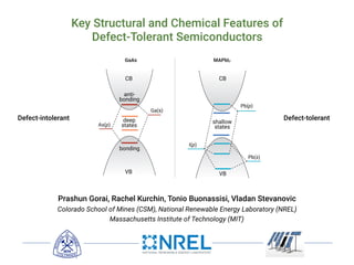
1. Prashun Gorai, Rachel Kurchin, Tonio Buonassisi, Vladan Stevanovic
Colorado School of Mines (CSM), National Renewable Energy Laboratory (NREL)
Massachusetts Institute of Technology (MIT)
Key Structural and Chemical Features of
Defect-Tolerant Semiconductors
GaAs
deep
states
VB
bonding
anti-
bonding
VB
CBCB
MAPbI3
shallow
states
I(p)
As(p)
Pb(p)
Ga(s)
Pb(s)
Defect-intolerant Defect-tolerant
2. Shallow Defect States Reduce Trap-Assisted Recombination
VB
ET
Ei
trap
CB
e-
h+
• Shockley-Read-Hall trap-assisted recombination rate1,2:
shallow traps are desirable for defect tolerance
• Recombination rate increases as ET - Ei decreases
• Other factors: capture cross-section, carrier mobility, trap
density
n, p = electron, hole concentrations, ni = intrinsic concentration
NT = trap density, vth = thermal velocity, 𝜎 = capture cross-section
USRH =
pn n2
i
p + n + 2nicosh Ei ET
kT
NTvth
<latexit sha1_base64="R6DCV0DMPEJolrgMQ+JuKT5LMVI=">AAACznicbVHbattAEF2rtzS9xEkf+7LUFBySGMkU2pdAaBuSh1Lcxk4MliPW65G1eLUSuyMTs4i+9sP6E/2FvrYf0JXtQux0YOFw5szMzplRLoVB3/9Z8+7df/Dw0dbj7SdPnz3fqe/uXZqs0Bx6PJOZ7o+YASkU9FCghH6ugaUjCVej6YcqfzUDbUSmujjPYZiyiRKx4AwdFdWve1GYMkx0ai++npf0mIaxZtzm6khF4rpd2vxAHbQd5plJQgkxNpeK00jQI3oadUs77ZahFpME98vPUXcWWUzK0IhJyqJ6w2/5i6B3QbACDbKKTrRb64fjjBcpKOSSGTMI/ByHlmkUXEK5HRYGcsanbAIDBxVLwQztwoiSvnbMmMaZdk8hXbC3KyxLjZmnI6esljabuYr8X25QYPxuaIXKCwTFl4PiQlLMaOUqHQsNHOXcAca1cH+lPGHOJnTer01Z9M6Br21ibwrlDB7DBivxBjVzpAFMmVDVVvZMSEkvmDL/eNewSjQ/iolAc/jJnVYdnmmA6f4tMXW3CDadvwsu263AbwVf3jRO3q+uskVeklekSQLylpyQc9IhPcLJD/KL/CZ/vI4380rv21Lq1VY1L8haeN//As0A5L0=</latexit><latexit sha1_base64="R6DCV0DMPEJolrgMQ+JuKT5LMVI=">AAACznicbVHbattAEF2rtzS9xEkf+7LUFBySGMkU2pdAaBuSh1Lcxk4MliPW65G1eLUSuyMTs4i+9sP6E/2FvrYf0JXtQux0YOFw5szMzplRLoVB3/9Z8+7df/Dw0dbj7SdPnz3fqe/uXZqs0Bx6PJOZ7o+YASkU9FCghH6ugaUjCVej6YcqfzUDbUSmujjPYZiyiRKx4AwdFdWve1GYMkx0ai++npf0mIaxZtzm6khF4rpd2vxAHbQd5plJQgkxNpeK00jQI3oadUs77ZahFpME98vPUXcWWUzK0IhJyqJ6w2/5i6B3QbACDbKKTrRb64fjjBcpKOSSGTMI/ByHlmkUXEK5HRYGcsanbAIDBxVLwQztwoiSvnbMmMaZdk8hXbC3KyxLjZmnI6esljabuYr8X25QYPxuaIXKCwTFl4PiQlLMaOUqHQsNHOXcAca1cH+lPGHOJnTer01Z9M6Br21ibwrlDB7DBivxBjVzpAFMmVDVVvZMSEkvmDL/eNewSjQ/iolAc/jJnVYdnmmA6f4tMXW3CDadvwsu263AbwVf3jRO3q+uskVeklekSQLylpyQc9IhPcLJD/KL/CZ/vI4380rv21Lq1VY1L8haeN//As0A5L0=</latexit><latexit sha1_base64="R6DCV0DMPEJolrgMQ+JuKT5LMVI=">AAACznicbVHbattAEF2rtzS9xEkf+7LUFBySGMkU2pdAaBuSh1Lcxk4MliPW65G1eLUSuyMTs4i+9sP6E/2FvrYf0JXtQux0YOFw5szMzplRLoVB3/9Z8+7df/Dw0dbj7SdPnz3fqe/uXZqs0Bx6PJOZ7o+YASkU9FCghH6ugaUjCVej6YcqfzUDbUSmujjPYZiyiRKx4AwdFdWve1GYMkx0ai++npf0mIaxZtzm6khF4rpd2vxAHbQd5plJQgkxNpeK00jQI3oadUs77ZahFpME98vPUXcWWUzK0IhJyqJ6w2/5i6B3QbACDbKKTrRb64fjjBcpKOSSGTMI/ByHlmkUXEK5HRYGcsanbAIDBxVLwQztwoiSvnbMmMaZdk8hXbC3KyxLjZmnI6esljabuYr8X25QYPxuaIXKCwTFl4PiQlLMaOUqHQsNHOXcAca1cH+lPGHOJnTer01Z9M6Br21ibwrlDB7DBivxBjVzpAFMmVDVVvZMSEkvmDL/eNewSjQ/iolAc/jJnVYdnmmA6f4tMXW3CDadvwsu263AbwVf3jRO3q+uskVeklekSQLylpyQc9IhPcLJD/KL/CZ/vI4380rv21Lq1VY1L8haeN//As0A5L0=</latexit><latexit sha1_base64="R6DCV0DMPEJolrgMQ+JuKT5LMVI=">AAACznicbVHbattAEF2rtzS9xEkf+7LUFBySGMkU2pdAaBuSh1Lcxk4MliPW65G1eLUSuyMTs4i+9sP6E/2FvrYf0JXtQux0YOFw5szMzplRLoVB3/9Z8+7df/Dw0dbj7SdPnz3fqe/uXZqs0Bx6PJOZ7o+YASkU9FCghH6ugaUjCVej6YcqfzUDbUSmujjPYZiyiRKx4AwdFdWve1GYMkx0ai++npf0mIaxZtzm6khF4rpd2vxAHbQd5plJQgkxNpeK00jQI3oadUs77ZahFpME98vPUXcWWUzK0IhJyqJ6w2/5i6B3QbACDbKKTrRb64fjjBcpKOSSGTMI/ByHlmkUXEK5HRYGcsanbAIDBxVLwQztwoiSvnbMmMaZdk8hXbC3KyxLjZmnI6esljabuYr8X25QYPxuaIXKCwTFl4PiQlLMaOUqHQsNHOXcAca1cH+lPGHOJnTer01Z9M6Br21ibwrlDB7DBivxBjVzpAFMmVDVVvZMSEkvmDL/eNewSjQ/iolAc/jJnVYdnmmA6f4tMXW3CDadvwsu263AbwVf3jRO3q+uskVeklekSQLylpyQc9IhPcLJD/KL/CZ/vI4380rv21Lq1VY1L8haeN//As0A5L0=</latexit>
1Shockley and Read, Phys. Rev. 87 (1952), 2Hall, Phys. Rev. 87 (1952)
/152
3. Heuristic Guidelines for Defect Tolerance
1Walsh and Zunger, Nat. Mater. 16 (2017); 2Zhang et al., Phys. Rev. B 57 (1998); 3Zakutayev et al., JPC Lett. 5 (2014)
/153
commentary
Instilling defect tolerance in
new compounds
Aron Walshand Alex Zunger
The properties of semiconducting solids are determined by the imperfections they contain. Established
physical phenomena can be converted into practical design principles for optimizing defects and doping
in a broad range of technology-enabling materials.
I
mpurities and defects in solids dictate their
physical properties. Such imperfections
come in a few fundamental flavours:
doping (conductivity-promoting) defects and
impurities can create free carriers that enable
electronics; ‘killer defects’ (deep, charged
recombination centres), on the other hand,
quench transport; and charge scattering
defects reduce mobility. Materials that cannot
be doped (most wide-gap insulators) or that
have vanishing free carrier mobility at room
temperature (many Mott insulators) are not
useful for many electronic and optoelectronic
technologies. Owing to the strong historical
interaction between the theory of defects
and doping of semiconductor-based
technologies — be they microelectronics,
photovoltaics, transparent conductors, light-
emitting diodes (LEDs), or, more recently,
spintronics — a lot has been understood
about the physics and properties of defects in
inorganic semiconductors.
New technologies are focusing attention
on less explored classes of compounds —
such as halide perovskites, metal–organic
frameworks, two-dimensional materials, and
topological insulators — where defects feature
in a leading role. For example, topological
insulators such as Bi2S3 are hardly insulators
because intrinsic defects render them n-type
in the bulk, placing the Fermi level inside the
bulk conduction band. Also, halide perovskite
solar cells have not been effectively doped and
the modern theory of defects in crystalline
solids, based on first-principles electronic
structure techniques, exposes phenomena
that can be converted into practical
approaches for optimizing a broad range of
technology-enabling materials. Calculation
of defect levels based on Greens functions3–5
progressed to supercell treatments including
a complete description of local structure
optimization, chemical potentials and
charge states6,7
. There are many routes
available to instilling defect tolerance in
new compounds, and the specific approach
can be adapted to the target material and
device. For applications that are limited by
electrical conductivity and mobility, including
transparent conductors and thermoelectric
devices, an optimal material would combine
high carrier concentrations with weak carrier
scattering. For light conversion in solar cells
and LEDs, non-radiative recombination
channels must be removed at all costs. In the
new generation of ‘quantum materials’ (such
as topological conductors, Weyl conductors
and high-TC superconductors), control of the
carrier concentrations is key, as the position
of the Fermi level determines whether specific
band structure features are accessible.
Realities of point defect behaviour
All solids in equilibrium contain intrinsic
defects. A compound may also contain
unintentional chemical impurities and
of point defects and their formation energy,
which depends on the parametric Fermi level
(EF) and the external conditions that control
the chemical potentials (μ) of the reactants6–9
.
The formation energies ΔHD,q(μ,EF) of defect
type D (for example, vacancy or interstitial) in
charge state q (donors when q > 0; acceptors
when q < 0) are not material constants but
depend on the growth environment.
Electron-producing donor defects such as
anion vacancies are difficult (easy) to form in
a semiconductor that is already electron-rich
(electron-poor) — that is, n-type (p-type).
In contrast, hole-producing acceptor defects
such as cation vacancies are difficult (easy)
to form in a semiconductor that is already
electron-poor (electron-rich). Likewise,
anion vacancies are difficult (easy) to form
under growth conditions that are anion-rich
(anion-poor), and the opposite holds for
cation vacancies.
These relationships decide if an impurity
contemplated by a researcher will either
successfully substitute a host atom or be
rejected. They determine which of the
possible host crystal sites will be substituted;
whether the impurity will be ionized and
contribute free carriers; if the generated
electrons or holes will be eliminated by
structural rearrangements; and, if charge
carriers survive such compensation, whether
they will be localized or delocalized. Such
physical processes were initially ignored
antimony
Sb3+
tin
Sn2+
indium
In1+
thallium
Tl1+
lead
Pb2+
bismuth
Bi3+
• Presence of partially-oxidized cations - anti-bonding top of valence band1,2,3
• Large dielectric constants - effective screening of charged defects
• Low carrier effective masses - high mobility, small polar formation avoided
heuristic guidelines are qualitative, role of crystal structure is not clear
4. Broad Search Based on Heuristic Guidelines
• Preliminary search based on heuristic guidelines
identified several candidates1:
• Binary halides: InI, TlI, PbI2, SnI2, SbI3, BiI3
• Chalcohalides: BiOI, BiSI, BiSeI, SbSI, SbSeI, …
Prospective Article
Identifying defect-tolerant semiconductors with high minority-carrier
lifetimes: beyond hybrid lead halide perovskites
Riley E. Brandt, Massachusetts Institute of Technology, 77 Massachusetts Avenue, Cambridge, Massachusetts 02139, USA
Vladan Stevanović, National Renewable Energy Laboratory, 15013 Denver West Parkway, Golden, Colorado 80401; Colorado School of Mines,
1500 Illinois Street, Golden, Colorado 80401, USA
David S. Ginley, National Renewable Energy Laboratory, 15013 Denver West Parkway, Golden, Colorado 80401, USA
Tonio Buonassisi, Massachusetts Institute of Technology, 77 Massachusetts Avenue, Cambridge, Massachusetts 02139, USA
Address all correspondence to Riley E. Brandt, Tonio Buonassisi at rbrandt@alum.mit.edu; buonassisi@mit.edu
(Received 27 March 2015; accepted 23 April 2015)
Abstract
The emergence of methyl-ammonium lead halide (MAPbX3) perovskites motivates the identification of unique properties giving rise to excep-
tional bulk transport properties, and identifying future materials with similar properties. Here, we propose that this “defect tolerance” emerges
from fundamental electronic-structure properties, including the orbital character of the conduction and valence band extrema, the charge-
carrier effective masses, and the static dielectric constant. We use MaterialsProject.org searches and detailed electronic-structure calculations
to demonstrate these properties in other materials than MAPbX3. This framework of materials discovery may be applied more broadly, to
accelerate discovery of new semiconductors based on emerging understanding of recent successes.
Introduction
Many semiconductors have been studied over the last century for
their possible use in photovoltaics (PVs), light-emitting diodes
(LEDs), computing devices, sensors, and detectors. Of these,
only a select few have achieved sufficient optoelectronic perfor-
mance to transition into industrial manufacturing, and their iden-
tification and development have been slow and mostly empirical.
Recently, high-throughput computation and a deeper under-
standing of the physics-based requirements for high performance
have created the potential for an accelerated identification of
functional materials with manufacturing potential. For example,
materials screening criteria have been proposed to better focus
the search for novel candidate PV materials; they include the op-
tical band-gap energy[1,2]
and abruptness of absorption onset,[3,4]
in addition to boundary conditions of elemental abundance,[5]
and manufacturing cost.[6,7]
However, many materials have
met these criteria and yet have not achieved industrially relevant
conversion efficiencies (in excess of 10–15%) due to low
minority-carrier lifetimes or diffusion lengths, e.g., in the case
of Cu2ZnSn(S,Se)4,[8]
SnS,[9]
and others.[10]
Meanwhile, PV de-
vices have emerged based on methyl-ammonium lead iodide
(MAPbI3) and closely related halides (herein referred to as
MAPbX3). MAPbI3 is a semiconductor, which has demonstrated
exceptional minority-carrier lifetimes of 280 ns (in the mixed
iodide–chloride composition)[11]
and diffusion lengths up to
175 μm,[12]
comparable with the best single-crystal semiconduc-
tors. This, in addition to meeting the criteria above, has resulted
in a dramatic realization of PV conversion efficiencies up to
20.1%[13,14]
in 2015, from <4% in 2009.[15]
This paper examines whether the dramatic success of
MAPbX3 in PVs can be used as a basis to expand design criteria
to identify new potential high-performance optoelectronic ma-
terials. One of the most compelling questions engendered by
MAPbX3 as an optoelectronic material is the degree to which
it is unique, and whether its success can lead to the identifica-
tion of materials with improved stability and lower toxicity, yet
similar high performance. Clearly, as in previous design criteria
the high optical absorption coefficient is important, but also es-
sential are the long carrier diffusion lengths observed in
MAPbX3, enabled by high minority-carrier lifetime (τ) and mo-
bility (μ).[11,16,17]
The importance of τ and μ for device perfor-
mance has been established[18]
for the most highly performing
PV materials, including silicon,[19]
cadmium telluride,[20,21]
copper indium gallium diselenide,[22]
and gallium arsenide.[23]
Oddly, these more direct transport parameters, τ and μ, are
not traditionally considered essential screening criteria for
novel candidate PV materials. This may be partially a conse-
quence of the difficulty in measuring and/or calculating these
parameters. The direct measurement of minority carrier τ and
μ requires ultrafast electronic or optical sensors to capture tran-
sients,[24–27]
or strong steady-state signals,[28,29]
and must be
performed with PV-device-relevant illumination conditions,
electrical fields, and transport directions. Calculating τ and μ
from first-principles is even more challenging, given the lack
of well-established and high-throughput methods to directly
calculate electron–phonon interactions and/or trap capture
cross-sections. Although it is possible to obtain some informa-
tion about carrier mobility from effective masses, and
MRS Communications (2015), 5, 265–275
doi:10.1557/mrc.2015.26
MRS COMMUNICATIONS • VOLUME 5 • ISSUE 2 • www.mrs.org/mrc ▪265
1Brandt et al., MRS Comm. 5 (2015); 2Brandt et al., Chem. Mater. 29 (2017)
Searching for “Defect-Tolerant” Photovoltaic Materials: Combined
Theoretical and Experimental Screening
Riley E. Brandt,*,†
Jeremy R. Poindexter,†
Prashun Gorai,‡,§
Rachel C. Kurchin,†
Robert L. Z. Hoye,†,@
Lea Nienhaus,†
Mark W. B. Wilson,†,#
J. Alexander Polizzotti,†
Raimundas Sereika,∥
Raimundas Žaltauskas,∥
Lana C. Lee,⊥
Judith L. MacManus-Driscoll,⊥
Moungi Bawendi,†
Vladan Stevanović,‡,§
and Tonio Buonassisi†
†
Massachusetts Institute of Technology, Cambridge, Massachusetts 02139, United States
‡
Colorado School of Mines, Golden, Colorado 80401, United States
§
National Renewable Energy Laboratory, Golden, Colorado 80401, United States
∥
Faculty of Science and Technology, Lithuanian University of Educational Sciences, Vilnius 08106, Lithuania
⊥
Department of Materials Science and Metallurgy, University of Cambridge, Cambridge CB3 0FE, United Kingdom
*S Supporting Information
ABSTRACT: Recently, we and others have proposed screening criteria for
“defect-tolerant” photovoltaic (PV) absorbers, identifying several classes of
semiconducting compounds with electronic structures similar to those of
hybrid lead−halide perovskites. In this work, we reflect on the accuracy and
prospects of these new design criteria through a combined experimental and
theoretical approach. We construct a model to extract photoluminescence
lifetimes of six of these candidate PV absorbers, including four (InI, SbSI,
SbSeI, and BiOI) for which time-resolved photoluminescence has not been
previously reported. The lifetimes of all six candidate materials exceed 1 ns, a
threshold for promising early stage PV device performance. However, there
are variations between these materials, and none achieve lifetimes as high as
those of the hybrid lead−halide perovskites, suggesting that the heuristics for
defect-tolerant semiconductors are incomplete. We explore this through first-
principles point defect calculations and Shockley−Read−Hall recombination
models to describe the variation between the measured materials. In light of these insights, we discuss the evolution of screening
criteria for defect tolerance and high-performance PV materials.
■ INTRODUCTION
Thin-film polycrystalline photovoltaic (PV) materials offer the
potential for lower-capital intensity manufacturing relative to
crystalline silicon PV, but only if they can achieve high PV
conversion efficiencies in excess of 20%.1,2
Long minority-
carrier lifetimes are necessary to achieve high efficiency, yet to
date, there have been only a few classes of polycrystalline
semiconductors that have demonstrated minority-carrier life-
times in excess of 1 ns.3
Three classes of thin-film PV absorbers
have achieved bulk lifetimes in excess of 100 ns, and they
materials: it allows power conversion efficiencies on the order
of 10% in materials with strong optical absorption and suggests
the potential for further improvements.3
Including InP and
other III−V materials, as well as the Cu2ZnSn(S,Se)4 family of
materials14
in addition to CIGS, CdTe, and LHPs, there are
several additional classes of thin-film inorganic (or hybrid
organic−inorganic) polycrystalline semiconductors that are
known to exceed this 1 ns threshold.
In prior work, we hypothesized that a promising path to
achieving these long lifetimes is through defect-tolerant
Article
pubs.acs.org/cm
• Candidates exhibit lifetimes >1 nanosecond2
but not comparable to MAPbI3:
■ RESULTS
Photoluminescence Lifetime. TRPL data for all six
materials are plotted in Figure 1. There is a clear variation in
the TRPL behavior across the materials tested, with
(CH NH ) Bi I and InI demonstrating the slowest decay,
however, all effective lifetimes as well as “slow” expo
time constants exceed 1 ns.
Defect Calculations. Figure 2 shows calculated
formation enthalpies as a function of Fermi level for I
Figure 1. TRPL decay curves of all six materials measured. Dashed gray lines represent biexponential fits to the data, while solid black lines
using a numerical model incorporating both Shockley−Read−Hall and radiative recombination (see the Supporting Information for det
estimated parameters). The fluence used was 20 nJ/cm2
for all traces except for those of (CH3NH3)3Bi2I9 (approximately 1 nJ/cm2
) and S
nJ/cm2
). Data for (CH3NH3)3Bi2I9 were reproduced with permission from ref 33.
Chemistry of Materials A
defect calculations can reveal the nature of defects
/154
5. First-principles Calculation of Defect Levels
∆HD,q
Fermi energy (EF
)
VBM
CBM
0 Eg
q=0
-2
shallow
+1
acceptor
donor
deep acceptor
donor
• Supercell approach with finite size corrections and GW-corrected band edges1
HD,q = ED,q Ehost +
X
i
niµi + qEF + Ecorr
1Lany and Zunger, Phys. Rev. B 78 (2008)
/155
6. Breakdown of the Heuristic Description in Binary Halides
Kurchin, Gorai, Buonassisi, Stevanovic, Chem. Mater. 30 (2018)
VI
VIn
InI
IIn
InI
-1
+1
-1
+2
-3
-2
0
1
2
3
0 1.0 2.0
VI
VTl
TlI
ITl
TlI
-1
+1
+1
-1
-2
-1
0
1
2
3
4
0 1.0 2.0
VI
VSn
ISn
SnI
-2
+1
-3
-2
-3
+3
-1
0
1
2
3
4
0 1.0 2.0
VI
VPb
PbI
IPb
-2
+1
+3
-3
-1
0
1
2
3
4
5
0 1.0 2.0
VI
VBi
BiI
IBi
-3+1
-1
+1
+3
-1
0
1
2
3
4
0 1.0 2.0
SnI2
PbI2
BiI3
EF
(eV) EF
(eV) EF
(eV)
∆HD,q
(eV)∆HD,q
(eV)
VI
VSb
+1
-3
ISb
SbI
-1
+1
-1
0
1
2
3
4
5
0 0.5 1.0 1.5 2.0
SbI3
deep defects are present in all the candidate materials
/156
7. Refined Understanding
/157
• Existing guidelines are based on chemistry - does not account for interactions of dangling bonds or
structural relaxation upon defect formation
prior understanding refined understanding
cation vacancy
A(p) A(p)-nn
VC states
deep
C(p)
C(s)
A(s)
A(p)
band gap
C(p)
C(s)
A(s)
VC states
shallow
orbital chemistry and structure likely play a role in defect tolerance
Kurchin, Gorai, Buonassisi, Stevanovic, Chem. Mater. 30 (2018)
8. Role of Orbital Alignment
/158
A(p)
C(p)
C(s)
A(p)-nnresonant
VC states
A(p) A(p)-nn
VC states
deep
C(p)
C(s)
A(s) A(s)
bad alignment better alignment
• Good energy alignment of anion (p) and cation (s) will push valence band maxima to higher energies
• Better alignment in InI, TlI: cation vacancies are shallow
partially oxidized cation + good energy alignment = shallow cation vacancies
Kurchin, Gorai, Buonassisi, Stevanovic, Chem. Mater. 30 (2018)
9. Role of Crystal Structure: Symmetry
/159
1Shi and Du, Phys. Rev. B 90 (2014); 2Kurchin, Gorai, Buonassisi, Stevanovic, Chem. Mater. 30 (2018)
• Crystal site symmetry can promote shallow anion vacancies e.g. CsCl structure type1,2
TlBr: conduction band edge
Tl
Br
• Anion vacancy is deep in rocksalt TlBr1 but shallow in CsCl structure
VBr
VTl
TlBr
BrTl
-1
+1
+2-2
HD,q(eV)
0
1
2
3
4
EF (eV)
0 1.0 2.0 3.0
TlBr (CsCl structure): I-rich
TlBr (CsCl structure)
10. Role of Crystal Structure: Symmetry
/1510
1Shi and Du, Phys. Rev. B 90 (2014); 2Kurchin, Gorai, Buonassisi, Stevanovic, Chem. Mater. 30 (2018)
suitable crystal site symmetry promotes shallow anion vacancies
• Crystal site symmetry can promote shallow anion vacancies e.g. CsCl structure type1,2
• Anion vacancy is deep in orthorhombic InI but shallow in CsCl structure
InI (hypo-CsCl structure)
VI
VIn
InI
IIn
-1
+1
+2
-2
ΔHD,q(eV)
−1
0
1
2
3
4
EF (eV)
0 0.5 1.0 1.5
VIVIn
InIIIn
-1
+1
-1
ΔHD,q(eV)
−1
0
1
2
3
4
EF (eV)
0 0.5 1.0 1.5 2.0
InI (orthorhombic)
11. Role of Crystal Structure: Coordination
/1511
• Low anion coordination + large cations promote shallow anion vacancies by creating spatial separation
• Hypothetical PbI2 in a Cu2O structure (2-fold coordinated I) has shallow iodine vacancies
HD,q(eV)
0
1
2
3
4
VI
VPb
IPb
-2
+1
-3
EF (eV)
0 0.5 1.0 1.5
PbI2 (hypo-Cu2O structure) conduction band edge
I
Pb
low anion coordination promotes shallow anion vacancies
Kurchin, Gorai, Buonassisi, Stevanovic, Chem. Mater. 30 (2018)
VI
VPb
PbI
IPb
-2
+1
+3
-3
-1
ΔHD,q(eV)
0
1
2
3
4
EF (eV)
0 0.5 1.0 1.5 2.0
PbI2 (native structure)
12. Tradeoffs and Other Features
/1512
• Chemical and structural features appear to operate
independently
• InI, TlI: ns2 cation, bad structure - shallow cation but deep
anion vacancies
• WO3: ns2 cation absent, good structure - deep cation
vacancies but shallow anion vacancies
VO
WO
OW
VW
WO3: O-rich
+2
-2
-3
-6
-1
-3
W
O
ΔHD,q(eV)
0
2
4
6
8
EF (eV)
0 0.5 1.0 1.5 2.0
Kurchin, Gorai, Buonassisi, Stevanovic, Chem. Mater. 30 (2018)
TlBr (225)
TlBr (221)
TlI (63)
TlI (221)
InI (63)
InI (221)
intolerant
tolerant
E-Evacuum(eV)
−8
−6
−4
−2
0
• Absolute band edge positions: CB edge lower in
defect-tolerant structures with shallow anion
vacancies
13. Defect-Tolerance in Ternary Semiconductors: MAPbI3
/1513
• Pseudo-binary: No MA contribution to band edges
1Miyata et al., Nature Physics 11 (2015)
• Heuristic guidelines:
Partially-oxidized cation: Pb2+
Large dielectric constants: MA dipole contributes
Low effective masses1: ~0.1 me
• Refined guidelines:
Orbital alignment sub-optimal: Pb(6s) and I(5p) but ..
Desirable structure: low anion coordination
Does MAPbI3 fair well within these refined guidelines?
VB
CB
MAPbI3
I(5p)
Pb(6p)
Eg
Pb(6s)
ternary and multinary semiconductors offer more tunability to satisfy these criteria
14. Extending the Refined Guidelines to Ternary Semiconductors
/1514
refined guidelines need to be further refined!
PbTlI3
Pb
Tl
I
• Preliminary search based on presence of ns2 cation and low anion coordination
VI
VTl
PbTlI3: I-rich
VPb
ΔHD,q(eV)
−1
0
1
2
3
EF (eV)
0 1 2
• PbTlI3: anion is 3-fold coordinated
• Iodine vacancies: states ~200 meV from band edges but low concentrations
• Conduction band: not just p states of ns2 cation - also I(p) states
15. Outlook
Funding and Computational Resources
National Science Foundation - SusChem
DOE Energy Frontier Research Center CNGMD
NREL High Performance Computing (HPC)
• A refined understanding of the chemical and structural features for defect tolerance
• Shallow cation vacancies: partially-oxidized cation + good energy alignment
• Shallow anion vacancies: suitable crystal site symmetry or low anion coordination
• Additional factors for defect tolerance to interstitials
• Extension of guidelines to ternary chemistries needs careful consideration