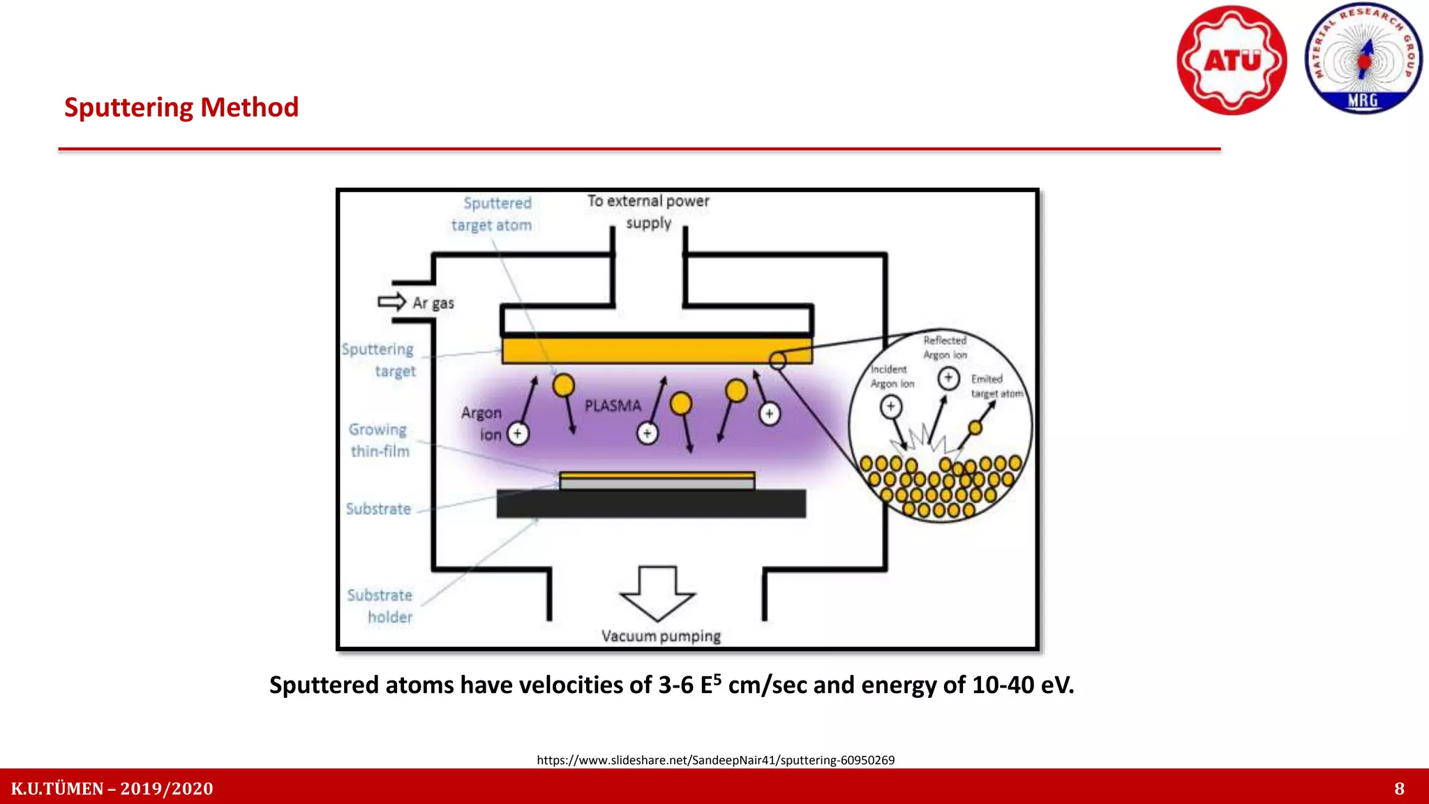
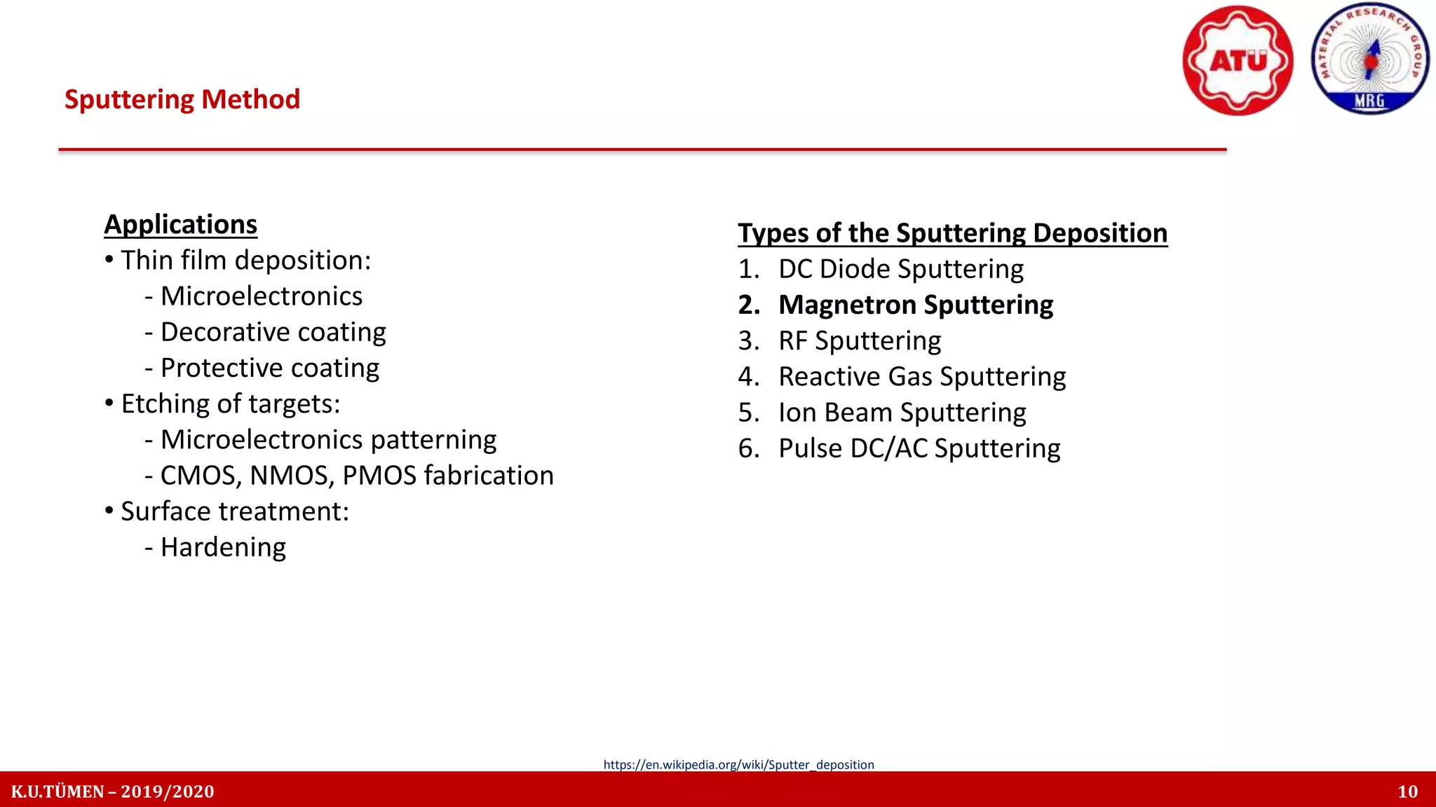
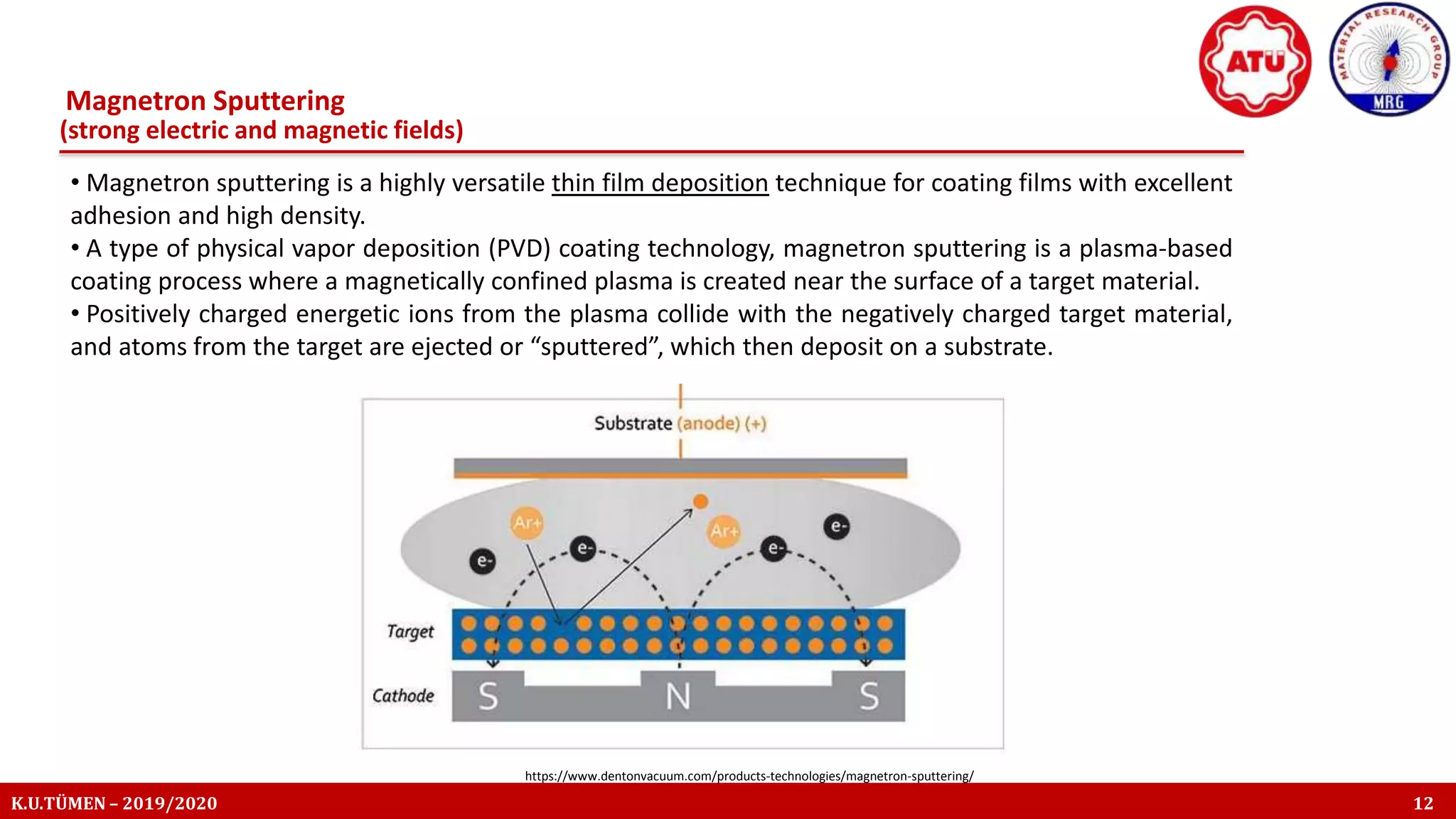
Kutluhan Utku TÜMEN
2019 / 2020
MAGNETRON SPUTTERING
- Thin Film
- Synthesis of Thin Films
- Plasma
- Physical Vapor Deposition
- Sputtering Method
- Magnetron Sputtering
Content
K.U.TÜMEN – 2019/2020 1
Thin Film
K.U.TÜMEN – 2019/2020 2
• A thin film is a layer of material ranging from fractions of a nanometer (monolayer) to several micrometers in
thickness.
•The act of applying a thin film to a surface is thin-film deposition – any technique for depositing a thin film of material
onto a substrate.
•It is useful in the manufacture of optics, electronics (layers of insulators, semiconductors, and conductors form
integrated circuits), packaging (i.e., aluminium-coated PET film).
https://en.wikipedia.org/wiki/Thin_film / https://www.avantes.com/solutions/thin-film 7 https://www.susumu.co.jp/germany/tech/know_how_02.php
Synthesis of Thin Films
K.U.TÜMEN – 2019/2020 3
https://www.researchgate.net/figure/Classification-of-thin-film-deposition-methods_fig3_320849346
Plasma
K.U.TÜMEN – 2019/2020 4
• States of Matter
- Solid
- Liquid
- Gas
- Plasma
https://www.nasa.gov/mission_pages/themis/auroras/sun_earth_connect.html
Physical Vapor Deposition
K.U.TÜMEN – 2019/2020 5
https://en.wikipedia.org/wiki/Physical_vapor_deposition
• Deposition of a material in the vapor phase onto a solid in a vacuum.
• The coating method involves purely physical processes such as high-
temperature vacuum evaporation with subsequent condensation, or plasma.
• Evaporated atoms travel through the evacuated space between the source
and the sample and stick to the sample.
• Usually no chemical reactions take place.
• Carried out in a vacuum atmosphere.
• Used for thin and uniform coating or films.
Sputtering Method
K.U.TÜMEN – 2019/2020 6
• Sputter deposition is a physical vapor deposition (PVD) method of thin film deposition by sputtering.
This involves ejecting material from a "target" that is a source onto a "substrate" such as a silicon wafer.
• First discovered in 1852, and developed as a thin film deposition technique by Langmuir in 1920.
• Metallic films: Al-alloys, Ti, Tantalum, Nickel, Cobalt, Gold, etc.
https://www.sciencedirect.com/topics/chemical-engineering/reactive-sputtering
• Requirements: Vacuum, Inert gas, Power supply, Sputtering gas
Sputtering Method
K.U.TÜMEN – 2019/2020 7
• Ionize an Ar; or ionize an impurity atom, for example O, to generate O- (for Ar, always positive ion Ar+ )
• Ions are generated and directed at a target.
• The ions sputter targets atoms.
• The ejected atoms are transported to the substrate.
• Atoms condense and form a thin film.
https://www.slideshare.net/HotLookingCoolGuy/sputtering-process
Sputtering Method
K.U.TÜMEN – 2019/2020 8
https://www.slideshare.net/SandeepNair41/sputtering-60950269
Sputtered atoms have velocities of 3-6 E5 cm/sec and energy of 10-40 eV.
Sputtering Yield
K.U.TÜMEN – 2019/2020 9
https://www.slideshare.net/SandeepNair41/sputtering-60950269
Mass & Size of Atoms
Molecule size – need to be about the same
size as the sputtered material
Energy of the Bombarding Ions
Ion energy Vs. sputter yield:
Direction
In oblique angle (45º-90º) there is
higher probability for sputtering, which
occur closer to the surface.
K.U.TÜMEN – 2019/2020 10
https://en.wikipedia.org/wiki/Sputter_deposition
Sputtering Method
Applications
• Thin film deposition:
- Microelectronics
- Decorative coating
- Protective coating
• Etching of targets:
- Microelectronics patterning
- CMOS, NMOS, PMOS fabrication
• Surface treatment:
- Hardening
Types of the Sputtering Deposition
1. DC Diode Sputtering
2. Magnetron Sputtering
3. RF Sputtering
4. Reactive Gas Sputtering
5. Ion Beam Sputtering
6. Pulse DC/AC Sputtering
K.U.TÜMEN – 2019/2020 11
https://www.physlab.org/wp-content/uploads/2016/04/Murtaza_presentaion.pdf
Magnetron Sputtering
• Here magnets are used to increase the percentage of electrons that take part in ionization events,
increase probability of electrons striking Ar, increase electron path length, so the ionization efficiency is
increased significantly.
• Another reasons to use magnets:
– Lower voltage needed to strike plasma.
– Controls uniformity.
– Reduce wafer heating from electron bombardment.
– Increased deposition rate
– Good control over reactive sputtering
Magnetron Sputtering
K.U.TÜMEN – 2019/2020 12
https://www.dentonvacuum.com/products-technologies/magnetron-sputtering/
• Magnetron sputtering is a highly versatile thin film deposition technique for coating films with excellent
adhesion and high density.
• A type of physical vapor deposition (PVD) coating technology, magnetron sputtering is a plasma-based
coating process where a magnetically confined plasma is created near the surface of a target material.
• Positively charged energetic ions from the plasma collide with the negatively charged target material,
and atoms from the target are ejected or “sputtered”, which then deposit on a substrate.
(strong electric and magnetic fields)
K.U.TÜMEN – 2019/2020 13
Magnetron Sputtering
https://farotex.com/technology.html
Magnetron Sputtering
K.U.TÜMEN – 2019/2020 14
The magnetron device has a dipole magnetic
configuration to trap the electrons emitted at
the cathode. In this way the excitation and
ionization rates are enhanced, allowing the
operation of the discharge at low pressures,
below 10-2 mbar. To create this dipole
configuration, usually three rows of permanent
magnets are arranged in the following order, N-
S-N or S-N-S, that is, the inner row must have
an opposite polarization in relation to the
outer rows. On the balanced magnetrons, the
magnets have the same strength. On the
unbalanced magnetron the inner magnet is
weakened. In this way, more electrons are lost
to the plasma, resulting in an increase of the
plasma length, towards the substrate. In this
way, the substrate current increases
dramatically, as well as the coating quality.
K.U.TÜMEN – 2019/2020 15
https://www.youtube.com/watch?v=ixx3ISj_kpg
THANK YOU
FOR
PARTICIPATING AND LISTENING
K.U.TÜMEN – 2019/2020 16

Magnetron sputtering

  • 1.
    Kutluhan Utku TÜMEN 2019/ 2020 MAGNETRON SPUTTERING
  • 2.
    - Thin Film -Synthesis of Thin Films - Plasma - Physical Vapor Deposition - Sputtering Method - Magnetron Sputtering Content K.U.TÜMEN – 2019/2020 1
  • 3.
    Thin Film K.U.TÜMEN –2019/2020 2 • A thin film is a layer of material ranging from fractions of a nanometer (monolayer) to several micrometers in thickness. •The act of applying a thin film to a surface is thin-film deposition – any technique for depositing a thin film of material onto a substrate. •It is useful in the manufacture of optics, electronics (layers of insulators, semiconductors, and conductors form integrated circuits), packaging (i.e., aluminium-coated PET film). https://en.wikipedia.org/wiki/Thin_film / https://www.avantes.com/solutions/thin-film 7 https://www.susumu.co.jp/germany/tech/know_how_02.php
  • 4.
    Synthesis of ThinFilms K.U.TÜMEN – 2019/2020 3 https://www.researchgate.net/figure/Classification-of-thin-film-deposition-methods_fig3_320849346
  • 5.
    Plasma K.U.TÜMEN – 2019/20204 • States of Matter - Solid - Liquid - Gas - Plasma https://www.nasa.gov/mission_pages/themis/auroras/sun_earth_connect.html
  • 6.
    Physical Vapor Deposition K.U.TÜMEN– 2019/2020 5 https://en.wikipedia.org/wiki/Physical_vapor_deposition • Deposition of a material in the vapor phase onto a solid in a vacuum. • The coating method involves purely physical processes such as high- temperature vacuum evaporation with subsequent condensation, or plasma. • Evaporated atoms travel through the evacuated space between the source and the sample and stick to the sample. • Usually no chemical reactions take place. • Carried out in a vacuum atmosphere. • Used for thin and uniform coating or films.
  • 7.
    Sputtering Method K.U.TÜMEN –2019/2020 6 • Sputter deposition is a physical vapor deposition (PVD) method of thin film deposition by sputtering. This involves ejecting material from a "target" that is a source onto a "substrate" such as a silicon wafer. • First discovered in 1852, and developed as a thin film deposition technique by Langmuir in 1920. • Metallic films: Al-alloys, Ti, Tantalum, Nickel, Cobalt, Gold, etc. https://www.sciencedirect.com/topics/chemical-engineering/reactive-sputtering • Requirements: Vacuum, Inert gas, Power supply, Sputtering gas
  • 8.
    Sputtering Method K.U.TÜMEN –2019/2020 7 • Ionize an Ar; or ionize an impurity atom, for example O, to generate O- (for Ar, always positive ion Ar+ ) • Ions are generated and directed at a target. • The ions sputter targets atoms. • The ejected atoms are transported to the substrate. • Atoms condense and form a thin film. https://www.slideshare.net/HotLookingCoolGuy/sputtering-process
  • 9.
    Sputtering Method K.U.TÜMEN –2019/2020 8 https://www.slideshare.net/SandeepNair41/sputtering-60950269 Sputtered atoms have velocities of 3-6 E5 cm/sec and energy of 10-40 eV.
  • 10.
    Sputtering Yield K.U.TÜMEN –2019/2020 9 https://www.slideshare.net/SandeepNair41/sputtering-60950269 Mass & Size of Atoms Molecule size – need to be about the same size as the sputtered material Energy of the Bombarding Ions Ion energy Vs. sputter yield: Direction In oblique angle (45º-90º) there is higher probability for sputtering, which occur closer to the surface.
  • 11.
    K.U.TÜMEN – 2019/202010 https://en.wikipedia.org/wiki/Sputter_deposition Sputtering Method Applications • Thin film deposition: - Microelectronics - Decorative coating - Protective coating • Etching of targets: - Microelectronics patterning - CMOS, NMOS, PMOS fabrication • Surface treatment: - Hardening Types of the Sputtering Deposition 1. DC Diode Sputtering 2. Magnetron Sputtering 3. RF Sputtering 4. Reactive Gas Sputtering 5. Ion Beam Sputtering 6. Pulse DC/AC Sputtering
  • 12.
    K.U.TÜMEN – 2019/202011 https://www.physlab.org/wp-content/uploads/2016/04/Murtaza_presentaion.pdf Magnetron Sputtering • Here magnets are used to increase the percentage of electrons that take part in ionization events, increase probability of electrons striking Ar, increase electron path length, so the ionization efficiency is increased significantly. • Another reasons to use magnets: – Lower voltage needed to strike plasma. – Controls uniformity. – Reduce wafer heating from electron bombardment. – Increased deposition rate – Good control over reactive sputtering
  • 13.
    Magnetron Sputtering K.U.TÜMEN –2019/2020 12 https://www.dentonvacuum.com/products-technologies/magnetron-sputtering/ • Magnetron sputtering is a highly versatile thin film deposition technique for coating films with excellent adhesion and high density. • A type of physical vapor deposition (PVD) coating technology, magnetron sputtering is a plasma-based coating process where a magnetically confined plasma is created near the surface of a target material. • Positively charged energetic ions from the plasma collide with the negatively charged target material, and atoms from the target are ejected or “sputtered”, which then deposit on a substrate. (strong electric and magnetic fields)
  • 14.
    K.U.TÜMEN – 2019/202013 Magnetron Sputtering https://farotex.com/technology.html
  • 15.
    Magnetron Sputtering K.U.TÜMEN –2019/2020 14 The magnetron device has a dipole magnetic configuration to trap the electrons emitted at the cathode. In this way the excitation and ionization rates are enhanced, allowing the operation of the discharge at low pressures, below 10-2 mbar. To create this dipole configuration, usually three rows of permanent magnets are arranged in the following order, N- S-N or S-N-S, that is, the inner row must have an opposite polarization in relation to the outer rows. On the balanced magnetrons, the magnets have the same strength. On the unbalanced magnetron the inner magnet is weakened. In this way, more electrons are lost to the plasma, resulting in an increase of the plasma length, towards the substrate. In this way, the substrate current increases dramatically, as well as the coating quality.
  • 16.
    K.U.TÜMEN – 2019/202015 https://www.youtube.com/watch?v=ixx3ISj_kpg
  • 17.
    THANK YOU FOR PARTICIPATING ANDLISTENING K.U.TÜMEN – 2019/2020 16