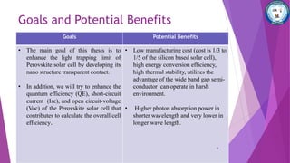
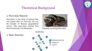
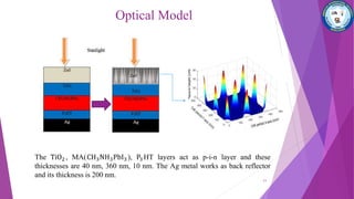
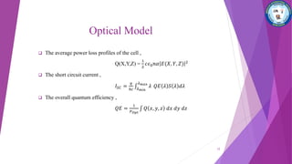
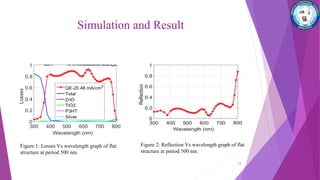
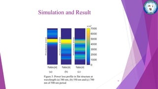
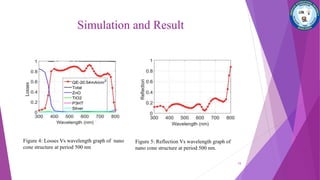
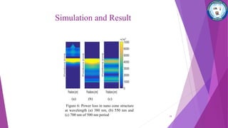
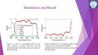
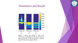
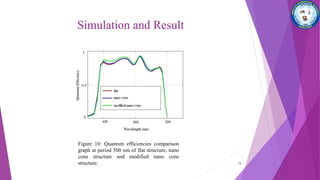
“Improvement of Light-Trapping in Perovskite
Solar Cell by Developing Nano-Structured
Transparent Contact.”
1
Final Defense
on
Group #61
Under the supervision of
Mohammad Ismail Hossain
Assistant professor, Faculty of Engineering
American International University - Bangladesh 2
Names ID
Islam, Rakibul 13-23758-1
Palash, Fazlul Karim 13-23775-1
Shamsuddin, MD. 13-23833-1
Sarker, Chinmoy 13-23797-1
Contents
 Introduction
 Goals and Potential Benefits
 Methodology for Achieving Goal
 Theoretical Background
 Optical Model
 Simulation Results
 Conclusion and Future Development
 References
3
Introduction
 Photovoltaics is the direct conversion of light into electricity.
 Some materials exhibit a property known as the photoelectric effect that causes
to absorb photons of light and release electrons.
 These free electrons are captured, an electric current results that can be used as
electricity
4
Reasons of becoming more research interest
Goals and Potential Benefits
Goals Potential Benefits
• The main goal of this thesis is to
enhance the light trapping limit of
Perovskite solar cell by developing its
nano structure transparent contact.
• In addition, we will try to enhance the
quantum efficiency (QE), short-circuit
current (Isc), and open circuit-voltage
(Voc) of the Perovskite solar cell that
contributes to calculate the overall cell
efficiency.
• Low manufacturing cost (cost is 1/3 to
1/5 of the silicon based solar cell),
high energy conversion efficiency,
high thermal stability, utilizes the
advantage of the wide band gap semi-
conductor can operate in harsh
environment.
• Higher photon absorption power in
shorter wavelength and very lower in
longer wave length.
6
Methodology for Achieving Goal
Flat structure perovskite
solar cell
Nano-cone (nano-wire)
textured perovskite solar cell
(opening angle 128 degree
and texture height 60 nm)
Simulation and results
Modified nano-cone (nano-
wire) textured perovskite
solar cell (opening angle 40
degree and texture height 340
nm)
7
Theoretical Background
Perovskite Solar Cells:
A perovskite solar cell (PSC) is a type of solar cell which includes
a perovskite structured compound, most commonly a hybrid organic-
inorganic lead or tin halide-based material, as the light-harvesting active layer.
For more than 7 years it has been under extensive research. It specially
attractive for Building Integrated Photovoltaic (BIPV).
PSCs is third generation solar cells which is based on Nano PV technology.
The PSCs are made up of five components:
 Conductive mechanical support
 Semiconductor film
 Perovskites
 Redox couple electrolyte and
 Counter electrode 8
 Perovskite Material:
Perovskite is one kind of mineral that
was named after Lev Perovski. He was
the founder of Russian geographical
society. This perovskite mineral first
discovered in the Ural Mountains.
 Basic Structure:
Naturally occurring Perovskite
9
Theoretical Background
Advantages & Limitations of Perovskite
Solar Cell
Advantages:
 Low cost
 Easy to handle
 Flexible
 More efficient in absorbing light
 Easy to setup
Limitations:
 Lead based Perovskite solar cells have
some effect on environment
10
Optical Model
The TiO2 , MA(CH3NH3PbI3 ), P3 HT layers act as p-i-n layer and these
thicknesses are 40 nm, 360 nm, 10 nm. The Ag metal works as back reflector
and its thickness is 200 nm.
11
Optical Model
 The average power loss profiles of the cell ,
Q(X,Y,Z) =
1
2
𝑐𝜖0 𝑛𝛼 𝐸(𝑋, 𝑌, 𝑍) 2
 The short circuit current ,
𝐼𝑆𝐶 =
𝑞
ℎ𝑐 𝜆 𝑚𝑖𝑛
𝜆 𝑚𝑎𝑥
𝜆 𝑄𝐸 𝜆 𝑆 𝜆 𝑑𝜆
 The overall quantum efficiency ,
𝑄𝐸 =
1
𝑃 𝑂𝑝𝑡
𝑄 𝑥, 𝑦, 𝑧 𝑑𝑥 𝑑𝑦 𝑑𝑧
12
Simulation and Result
Figure 1: Losses Vs wavelength graph of flat
structure at period 500 nm.
Figure 2: Reflection Vs wavelength graph of flat
structure at period 500 nm.
13
Simulation and Result
(a) (b) (c)
Figure 3: Power loss profile in flat structure at
wavelength (a) 380 nm, (b) 550 nm and (c) 700
nm of 500 nm period
14
Simulation and Result
Figure 4: Losses Vs wavelength graph of nano
cone structure at period 500 nm
Figure 5: Reflection Vs wavelength graph of
nano cone structure at period 500 nm.
15
Simulation and Result
(a) (b) (c)
Figure 6: Power loss in nano cone structure
at wavelength (a) 380 nm, (b) 550 nm and
(c) 700 nm of 500 nm period 16
Simulation and Result
Figure 7: Losses Vs wavelength graph of nano
cone structure at period 500 nm and the
conduction angle and texture height are respect to
400 and 340 nm.
Figure 8: Reflection Vs wavelength graph of nano
cone structure at period 500 nm and the
conduction angle and texture height are respect to
400 and 340 nm. 17
Simulation and Result
(a) (b) (c)
Figure 9: Power loss profile in nano cone
structure at wavelength (a) 380 nm, (b) 550 nm
and (c) 700 nm of 500 nm period at opening
angle 400 and texture height 340 nm.
18
Simulation and Result
Figure 10: Quantum efficiencies comparison
graph at period 500 nm of flat structure, nano
cone structure and modified nano cone
structure. 19
Conclusion and Future Development
Conclusion:
 In our thesis we developed the light trapping in perovskite solar cell by
texturing FTCO.
Future Development:
 Lead free Perovskite solar cell
 Textured structure will be developed in different layers
20
References
1. Susannah Lee,“Harvesting Solar Energy Using Inexpensive and Benign Materials,” Susannah Lee,2012. [Online].
Available:http://link.springer.com/referenceworkentry/10.1007/978-1-4419-7991-9_32. Accessed: Nov. 24, 2016.
2. Kojima, et al. “T. Organometal halide perovskites as visible-light sensitizers for photovoltaic cells,” J. Am. Chem.
Soc. 131, 6050–6051 (2009).
3. Kojima, et al. (May 6, 2009), “Organometal Halide Perovskites as Visible-Light Sensitizers for Photovoltaic
Cells,” Journal of the American Chemical Society. 131 (17): 60506051.
4. “Posts - EPFL Perovskite solar cell 21% efficiency entry in NREL efficiency chart,” 2015. [Online]. Available:
http://www.dyesol.com/posts/cat/corporatenews/post/EPFL_Perovskite_solar_cell_21_percent_efficiency_entry_in_N
REL_efficiency_chart/?___SID=U. Accessed: Nov. 24, 2016.
5. Ossila, “Perovskites and Perovskite solar cells: An introduction,” Ossila, 2015. [Online]. Available:
https://www.ossila.com/pages/perovskites-and-perovskite-solar-cells-an-introduction.Accessed: Nov. 24, 2016.
6. R.Dewan, , I. Vasilev And D. Knipp, “Optics in thin-film silicon solar cells with periodic surface texture,” 12th
Euregional Workshop on Novel Concepts for Future Thin-Film Silicon Solar Cells (Tu Delft, The Netherlands, 2010).
7. Burschka, et al. (July 10, 2013), “Sequential deposition as a route to high-performance perovskite-sensitized solar
cells,” Nature. 499 (7458): 316–319.
21
Any Question
22
23
The slides have been prepared by Fazlul Karim Palash

Presentation on Perovskite Solar Cell.

  • 1.
    “Improvement of Light-Trappingin Perovskite Solar Cell by Developing Nano-Structured Transparent Contact.” 1 Final Defense on
  • 2.
    Group #61 Under thesupervision of Mohammad Ismail Hossain Assistant professor, Faculty of Engineering American International University - Bangladesh 2 Names ID Islam, Rakibul 13-23758-1 Palash, Fazlul Karim 13-23775-1 Shamsuddin, MD. 13-23833-1 Sarker, Chinmoy 13-23797-1
  • 3.
    Contents  Introduction  Goalsand Potential Benefits  Methodology for Achieving Goal  Theoretical Background  Optical Model  Simulation Results  Conclusion and Future Development  References 3
  • 4.
    Introduction  Photovoltaics isthe direct conversion of light into electricity.  Some materials exhibit a property known as the photoelectric effect that causes to absorb photons of light and release electrons.  These free electrons are captured, an electric current results that can be used as electricity 4
  • 5.
    Reasons of becomingmore research interest
  • 6.
    Goals and PotentialBenefits Goals Potential Benefits • The main goal of this thesis is to enhance the light trapping limit of Perovskite solar cell by developing its nano structure transparent contact. • In addition, we will try to enhance the quantum efficiency (QE), short-circuit current (Isc), and open circuit-voltage (Voc) of the Perovskite solar cell that contributes to calculate the overall cell efficiency. • Low manufacturing cost (cost is 1/3 to 1/5 of the silicon based solar cell), high energy conversion efficiency, high thermal stability, utilizes the advantage of the wide band gap semi- conductor can operate in harsh environment. • Higher photon absorption power in shorter wavelength and very lower in longer wave length. 6
  • 7.
    Methodology for AchievingGoal Flat structure perovskite solar cell Nano-cone (nano-wire) textured perovskite solar cell (opening angle 128 degree and texture height 60 nm) Simulation and results Modified nano-cone (nano- wire) textured perovskite solar cell (opening angle 40 degree and texture height 340 nm) 7
  • 8.
    Theoretical Background Perovskite SolarCells: A perovskite solar cell (PSC) is a type of solar cell which includes a perovskite structured compound, most commonly a hybrid organic- inorganic lead or tin halide-based material, as the light-harvesting active layer. For more than 7 years it has been under extensive research. It specially attractive for Building Integrated Photovoltaic (BIPV). PSCs is third generation solar cells which is based on Nano PV technology. The PSCs are made up of five components:  Conductive mechanical support  Semiconductor film  Perovskites  Redox couple electrolyte and  Counter electrode 8
  • 9.
     Perovskite Material: Perovskiteis one kind of mineral that was named after Lev Perovski. He was the founder of Russian geographical society. This perovskite mineral first discovered in the Ural Mountains.  Basic Structure: Naturally occurring Perovskite 9 Theoretical Background
  • 10.
    Advantages & Limitationsof Perovskite Solar Cell Advantages:  Low cost  Easy to handle  Flexible  More efficient in absorbing light  Easy to setup Limitations:  Lead based Perovskite solar cells have some effect on environment 10
  • 11.
    Optical Model The TiO2, MA(CH3NH3PbI3 ), P3 HT layers act as p-i-n layer and these thicknesses are 40 nm, 360 nm, 10 nm. The Ag metal works as back reflector and its thickness is 200 nm. 11
  • 12.
    Optical Model  Theaverage power loss profiles of the cell , Q(X,Y,Z) = 1 2 𝑐𝜖0 𝑛𝛼 𝐸(𝑋, 𝑌, 𝑍) 2  The short circuit current , 𝐼𝑆𝐶 = 𝑞 ℎ𝑐 𝜆 𝑚𝑖𝑛 𝜆 𝑚𝑎𝑥 𝜆 𝑄𝐸 𝜆 𝑆 𝜆 𝑑𝜆  The overall quantum efficiency , 𝑄𝐸 = 1 𝑃 𝑂𝑝𝑡 𝑄 𝑥, 𝑦, 𝑧 𝑑𝑥 𝑑𝑦 𝑑𝑧 12
  • 13.
    Simulation and Result Figure1: Losses Vs wavelength graph of flat structure at period 500 nm. Figure 2: Reflection Vs wavelength graph of flat structure at period 500 nm. 13
  • 14.
    Simulation and Result (a)(b) (c) Figure 3: Power loss profile in flat structure at wavelength (a) 380 nm, (b) 550 nm and (c) 700 nm of 500 nm period 14
  • 15.
    Simulation and Result Figure4: Losses Vs wavelength graph of nano cone structure at period 500 nm Figure 5: Reflection Vs wavelength graph of nano cone structure at period 500 nm. 15
  • 16.
    Simulation and Result (a)(b) (c) Figure 6: Power loss in nano cone structure at wavelength (a) 380 nm, (b) 550 nm and (c) 700 nm of 500 nm period 16
  • 17.
    Simulation and Result Figure7: Losses Vs wavelength graph of nano cone structure at period 500 nm and the conduction angle and texture height are respect to 400 and 340 nm. Figure 8: Reflection Vs wavelength graph of nano cone structure at period 500 nm and the conduction angle and texture height are respect to 400 and 340 nm. 17
  • 18.
    Simulation and Result (a)(b) (c) Figure 9: Power loss profile in nano cone structure at wavelength (a) 380 nm, (b) 550 nm and (c) 700 nm of 500 nm period at opening angle 400 and texture height 340 nm. 18
  • 19.
    Simulation and Result Figure10: Quantum efficiencies comparison graph at period 500 nm of flat structure, nano cone structure and modified nano cone structure. 19
  • 20.
    Conclusion and FutureDevelopment Conclusion:  In our thesis we developed the light trapping in perovskite solar cell by texturing FTCO. Future Development:  Lead free Perovskite solar cell  Textured structure will be developed in different layers 20
  • 21.
    References 1. Susannah Lee,“HarvestingSolar Energy Using Inexpensive and Benign Materials,” Susannah Lee,2012. [Online]. Available:http://link.springer.com/referenceworkentry/10.1007/978-1-4419-7991-9_32. Accessed: Nov. 24, 2016. 2. Kojima, et al. “T. Organometal halide perovskites as visible-light sensitizers for photovoltaic cells,” J. Am. Chem. Soc. 131, 6050–6051 (2009). 3. Kojima, et al. (May 6, 2009), “Organometal Halide Perovskites as Visible-Light Sensitizers for Photovoltaic Cells,” Journal of the American Chemical Society. 131 (17): 60506051. 4. “Posts - EPFL Perovskite solar cell 21% efficiency entry in NREL efficiency chart,” 2015. [Online]. Available: http://www.dyesol.com/posts/cat/corporatenews/post/EPFL_Perovskite_solar_cell_21_percent_efficiency_entry_in_N REL_efficiency_chart/?___SID=U. Accessed: Nov. 24, 2016. 5. Ossila, “Perovskites and Perovskite solar cells: An introduction,” Ossila, 2015. [Online]. Available: https://www.ossila.com/pages/perovskites-and-perovskite-solar-cells-an-introduction.Accessed: Nov. 24, 2016. 6. R.Dewan, , I. Vasilev And D. Knipp, “Optics in thin-film silicon solar cells with periodic surface texture,” 12th Euregional Workshop on Novel Concepts for Future Thin-Film Silicon Solar Cells (Tu Delft, The Netherlands, 2010). 7. Burschka, et al. (July 10, 2013), “Sequential deposition as a route to high-performance perovskite-sensitized solar cells,” Nature. 499 (7458): 316–319. 21
  • 22.
  • 23.
    23 The slides havebeen prepared by Fazlul Karim Palash