Download as PDF, PPTX


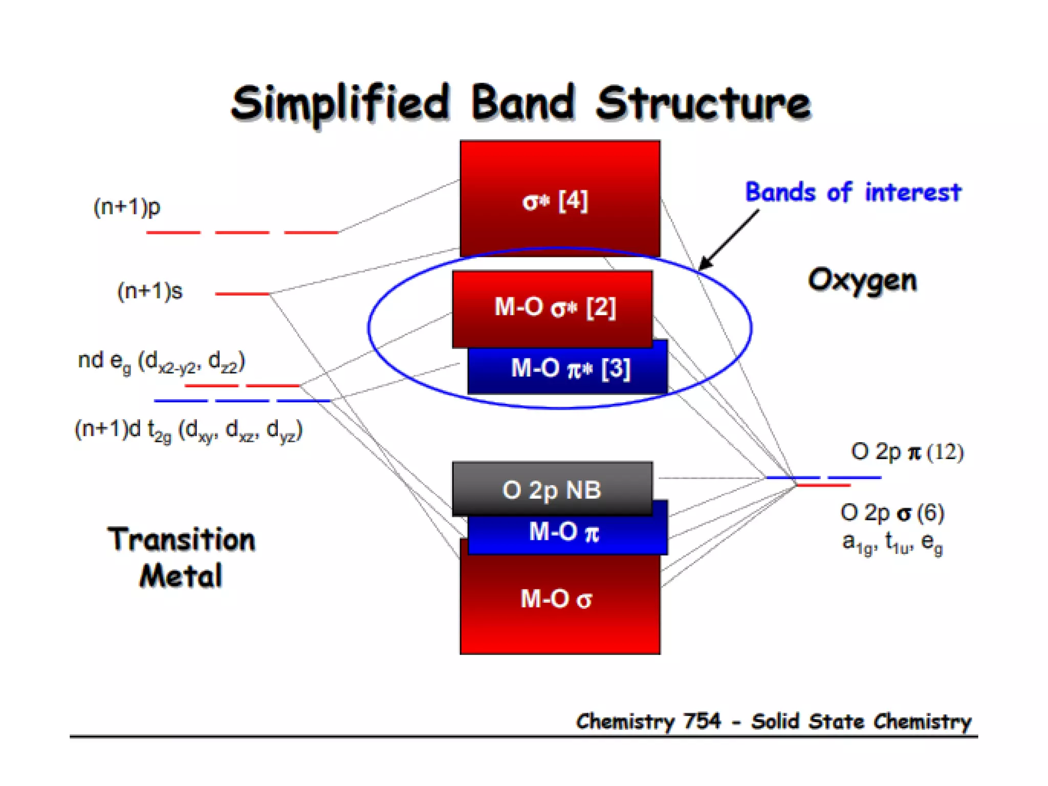
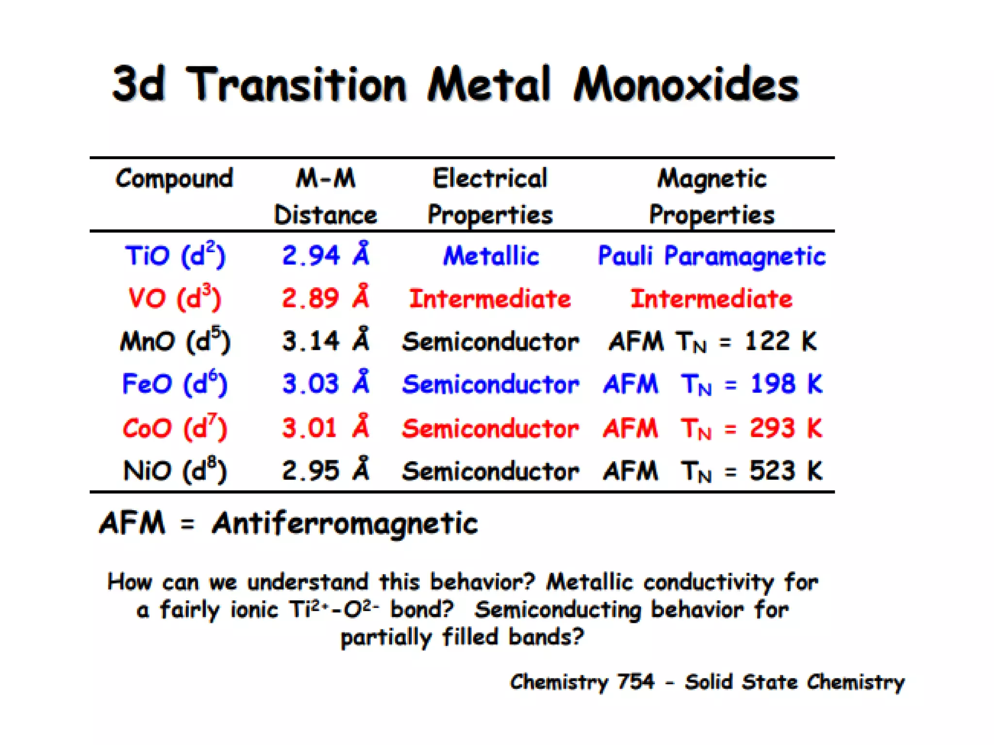


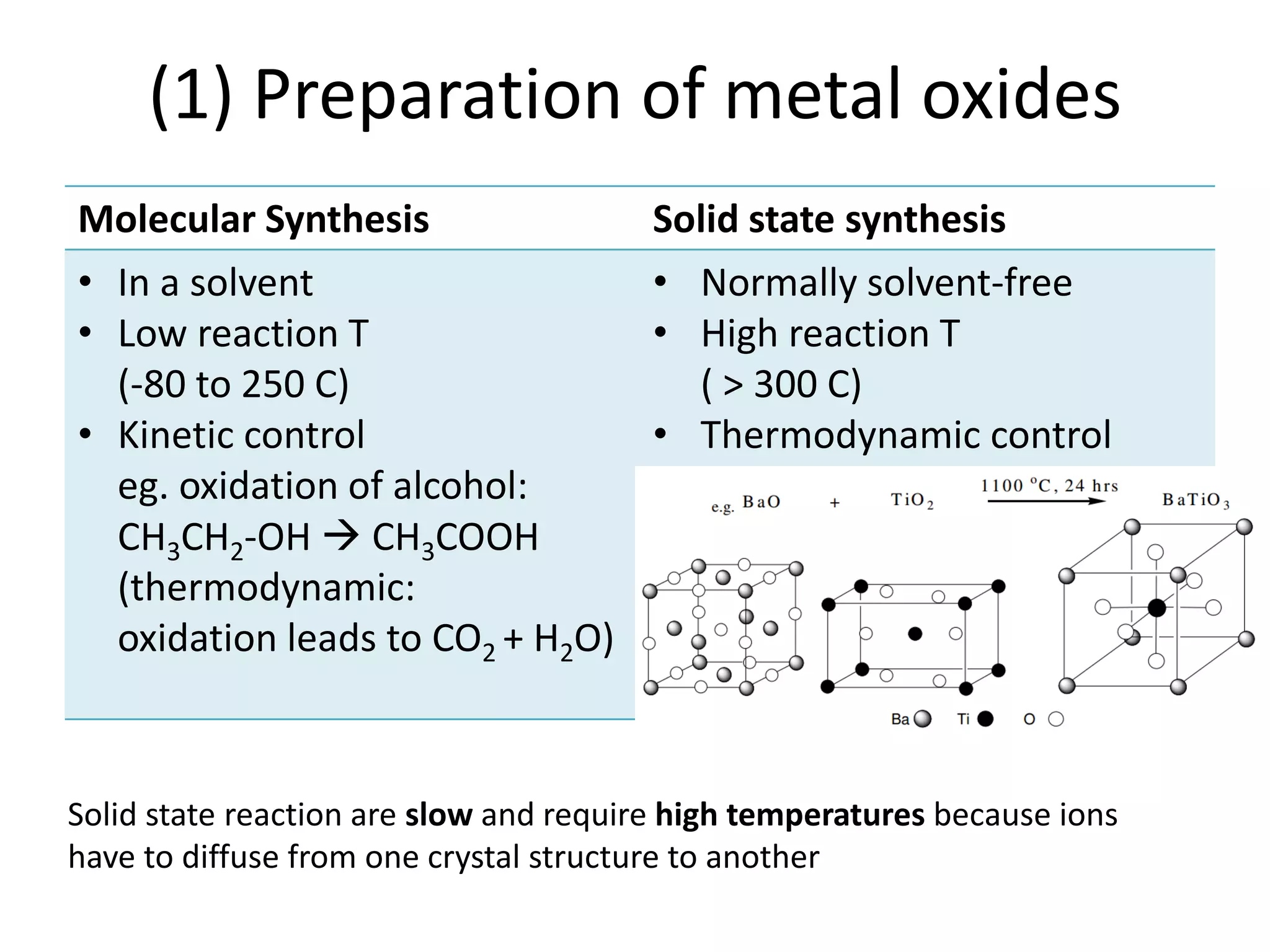


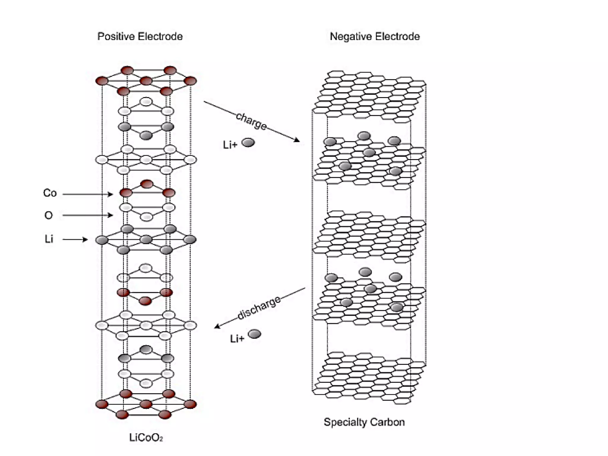
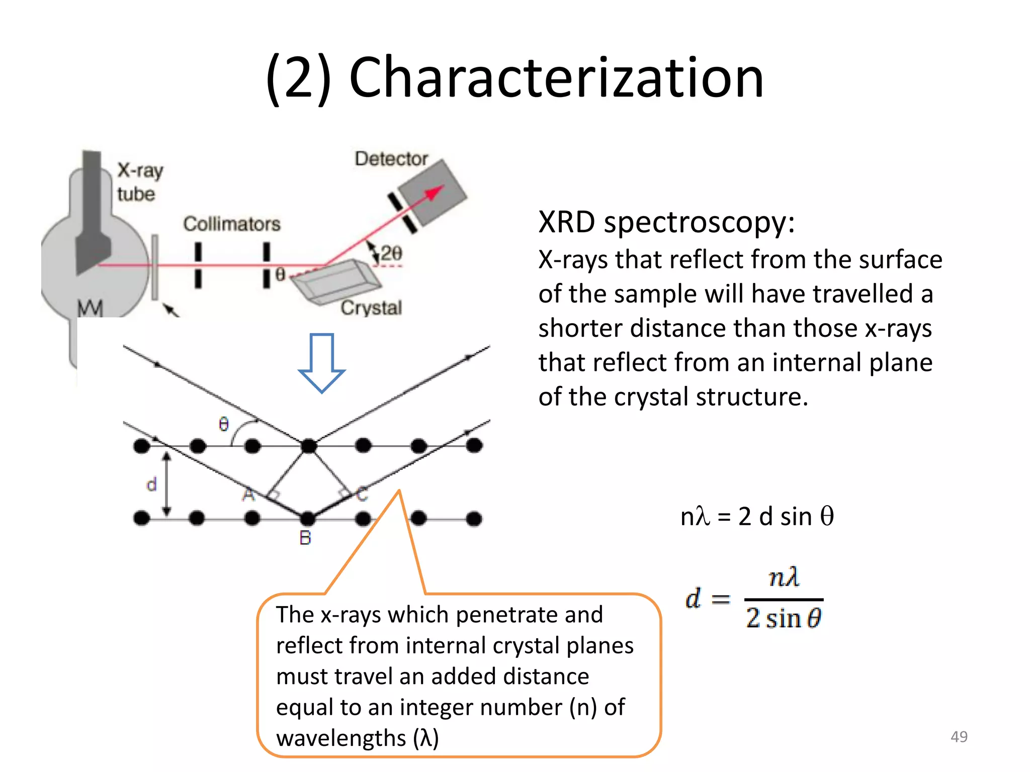


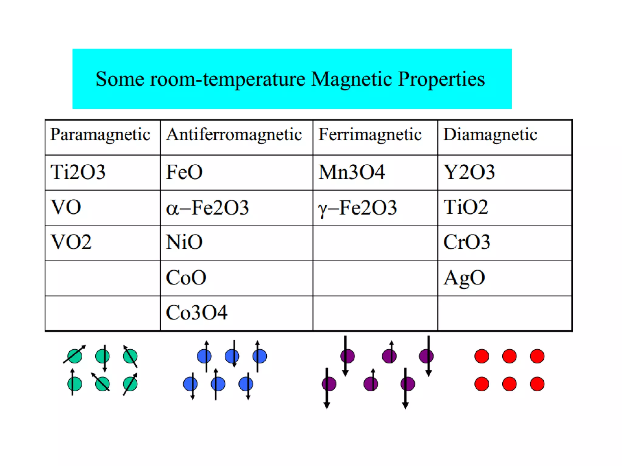


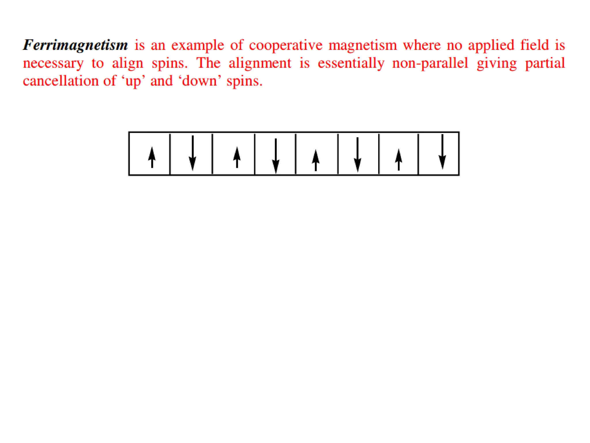
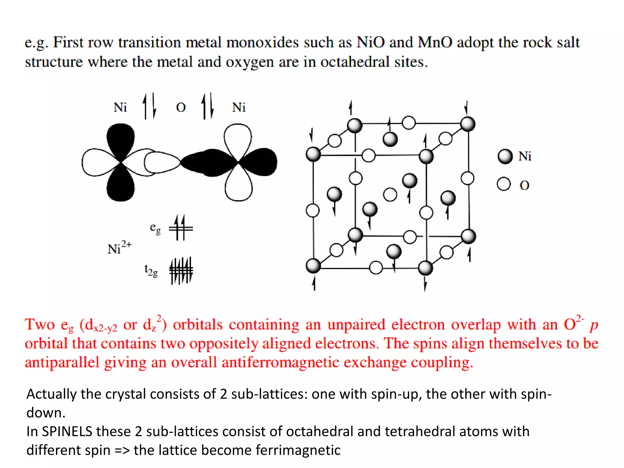

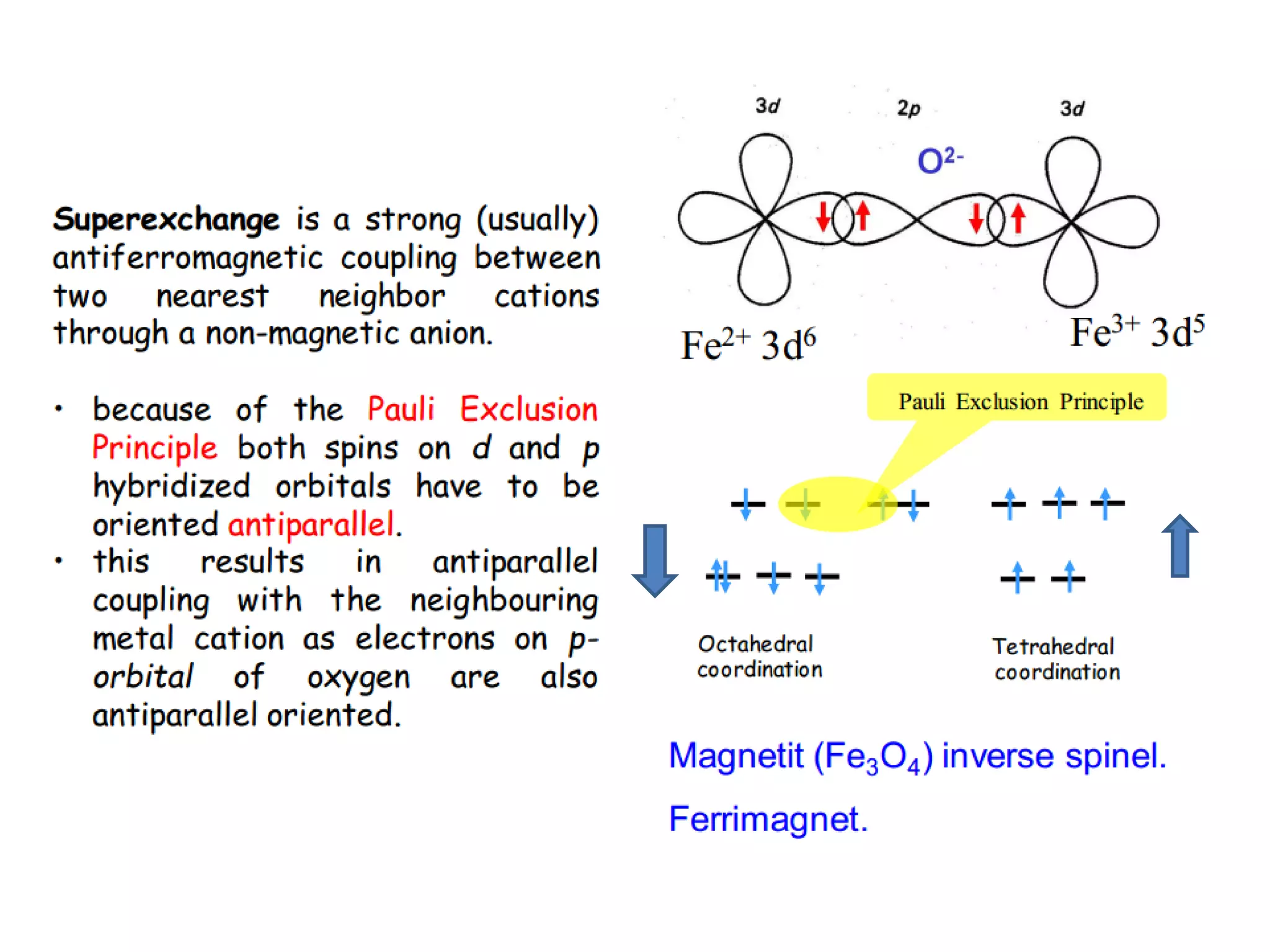
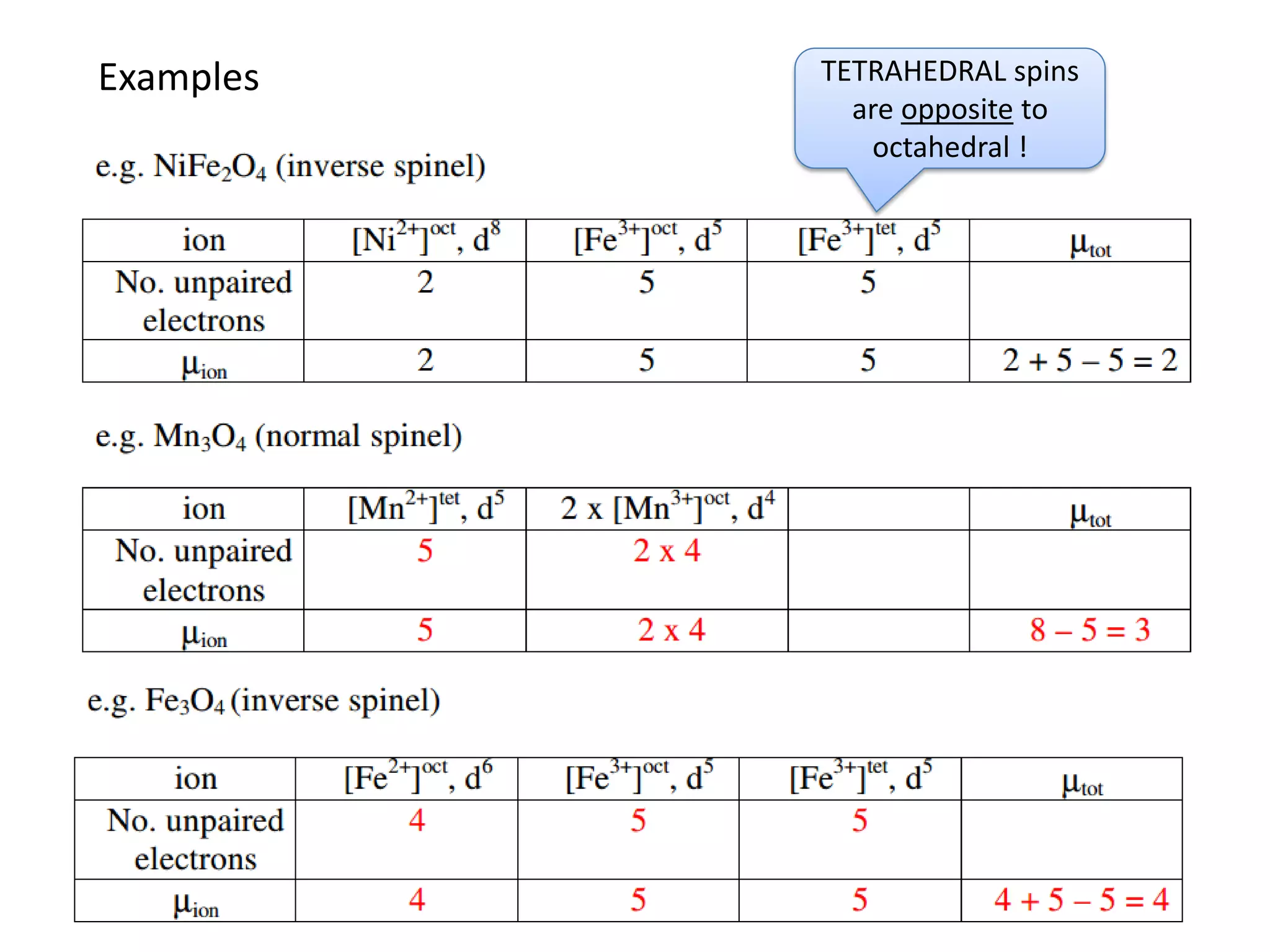

(1) The document discusses doping of semiconductors and transition metal oxides, including n-type and p-type doping of silicon. It also covers band structure diagrams and density of states plots. (2) Preparation methods for metal oxides include molecular synthesis and solid state synthesis. Modification of solids can occur through ion exchange or intercalation. Lithium ion batteries operate through lithium intercalation into graphite. (3) Characterization techniques covered are XRD for crystal structure analysis and electron microscopy. Magnetic properties depend on temperature; ferromagnets become paramagnetic above the Curie temperature. Spinels can exhibit ferrimagnetism from opposing sublattice


