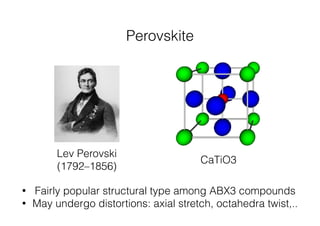
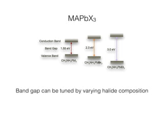
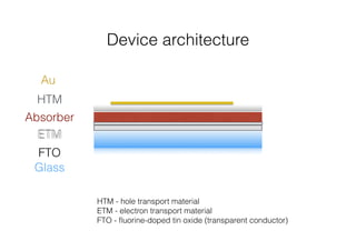
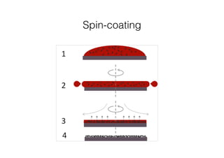
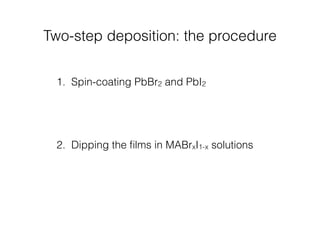
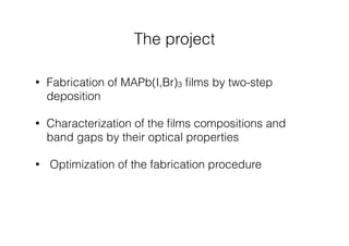
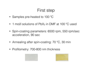
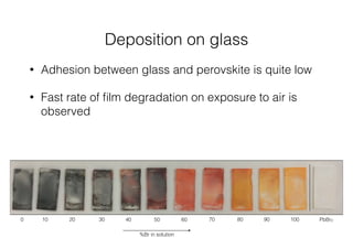
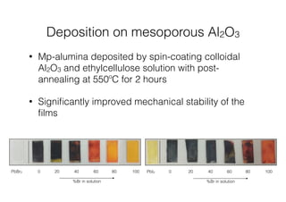
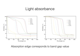
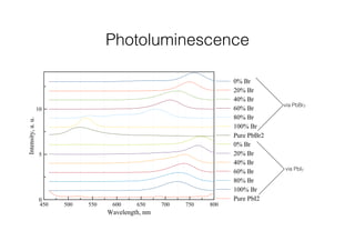
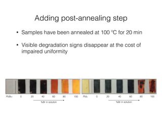
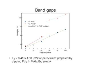
Band gap engineering of 
hybrid organic inorganic 
lead-halide perovskites 
Kirill Popov 
David Cahen Group 
Department of Materials and Interfaces
What is a band?
Band structure of solids
Key band positioning types
The principle of photovoltaics
Solar radiation 
Maximum in spectrum ∽ semiconductors band gap
Energy loss pathways 
• Radiative recombination 
• Relaxation to band edges 
• Blackbody radiation 
• Solar spectrum is not uniform 
• Other: non-radiative 
recombination, finite mobility
Energy loss pathways 
• Radiative recombination 
• Relaxation to band edges 
• Blackbody radiation 
• Solar spectrum is not uniform 
• Other: non-radiative 
recombination, finite mobility
Energy loss pathways 
• Radiative recombination 
• Relaxation to band edges 
• Blackbody radiation 
• Solar spectrum is not uniform 
• Other: non-radiative 
recombination, finite mobility
Shockley-Queisser Limit
Shockley-Queisser Limit 
33.7% for Egap 
of 1.34 eV
How to overcome the limit?
How to overcome the limit? 
Multijunction solar cells: 
«stacking»
Perovskite 
CaTiO3 
Lev Perovski 
(1792–1856) 
• Fairly popular structural type among ABX3 compounds 
• May undergo distortions: axial stretch, octahedra twist,..
Hybrid lead halide perovskites 
•Several easy preparation techniques exist 
•Cheap precursors, no rare elements 
•Relatively good conductance
MAPbX3 
Band gap can be tuned by varying halide composition
Device efficiency 
x
Device efficiency 
x 
Recent reports of 19.3% efficiency!
Device architecture 
Au 
HTM 
Absorber 
ETM 
FTO 
Glass 
HTM - hole transport material 
ETM - electron transport material 
FTO - fluorine-doped tin oxide (transparent conductor)
Spin-coating
Two-step deposition: the procedure 
1. Spin-coating PbBr2 and PbI2 
2. Dipping the films in MABrxI1-x solutions
The project 
• Fabrication of MAPb(I,Br)3 films by two-step 
deposition 
• Characterization of the films compositions and 
band gaps by their optical properties 
• Optimization of the fabrication procedure
First step 
• Samples pre-heated to 100 ºC 
• 1 mol/l solutions of PbX2 in DMF at 100 ºC used 
• Spin-coating parameters: 6500 rpm, 550 rpm/sec 
acceleration, 90 sec 
• Annealing after spin-coating: 70 ºC, 30 min 
• Profilometry: 700-800 nm thickness
Second step 
• Solution of MABr and MAI in iPrOH 
• C (total) = C (MA+) = 0.05 mol/l 
• 1h dipping time
Deposition on glass 
• Adhesion between glass and perovskite is quite low 
• Fast rate of film degradation on exposure to air is 
observed 
0 10 20 30 40 50 60 70 80 90 100 PbBr2 
%Br in solution
Deposition on mesoporous Al2O3 
• Mp-alumina deposited by spin-coating colloidal 
Al2O3 and ethylcellulose solution with post-annealing 
at 550ºC for 2 hours 
• Significantly improved mechanical stability of the 
films 
PbBr2 0 20 40 60 80 100 
%Br in solution 
0 20 40 60 80 100 
%Br in solution 
PbI2
Light absorbance 
Absorption edge corresponds to band gap value
Photoluminescence 
via PbBr2 
via PbI2
Band gap values 
• JH Noh et al.: Eg = 1.57 + 0.39x + 0.33x2 (eV) for MAPb(I1-xBrx)3 
• Eg = 1.54 + 0.16x + 0.45x2 (eV) for films prepared by dipping PbI2 in MAI1-xBrx solution
Adding post-annealing step 
• Samples have been annealed at 100 ºC for 20 min 
• Visible degradation signs disappear at the cost of 
impaired uniformity 
PbBr2 0 20 40 60 80 100 
%Br in solution 
0 20 40 60 80 100 
%Br in solution 
PbI2
Band gaps 
• Eg = 0.41x+1.53 (eV) for perovskites prepared by 
dipping PbI2 in MAI1-xBrx solution
Conclusions 
• Methyl ammonium lead iodide bromide band gap may be engineered 
between 1.55 and 2.29 eV by changing solution composition in two-step 
deposition process 
• Perovskite films are significantly less likely to be damaged mechanically if 
mesoporous scaffold is used 
• Tetragonal MAPbI3 phase formation is found to be preferable at all anion 
compositions of dipping solution 
• Annealing perovskites after dipping prevents instant degradation but 
affects uniform film formation process 
• Annealing converts quadratic dependence of band gap value on solution 
composition to linear
Future directions 
• Elemental and phase characterization of the films 
• Investigation into film degradation and its effect 
perovskite electronic structure 
• Unfixing different parameters - total concentration, 
time, annealing temperature etc.
Thanks 
Igal Levine 
Professor David Cahen and his group 
Professor Gary Hodes and his group 
Kupcinet-Getz Summer Program

Band gap engineering of hybrid perovskites for solar cells

  • 1.
    Band gap engineeringof hybrid organic inorganic lead-halide perovskites Kirill Popov David Cahen Group Department of Materials and Interfaces
  • 2.
    What is aband?
  • 3.
  • 4.
  • 5.
  • 6.
    The principle ofphotovoltaics
  • 7.
    Solar radiation Maximumin spectrum ∽ semiconductors band gap
  • 8.
    Energy loss pathways • Radiative recombination • Relaxation to band edges • Blackbody radiation • Solar spectrum is not uniform • Other: non-radiative recombination, finite mobility
  • 9.
    Energy loss pathways • Radiative recombination • Relaxation to band edges • Blackbody radiation • Solar spectrum is not uniform • Other: non-radiative recombination, finite mobility
  • 10.
    Energy loss pathways • Radiative recombination • Relaxation to band edges • Blackbody radiation • Solar spectrum is not uniform • Other: non-radiative recombination, finite mobility
  • 11.
  • 12.
    Shockley-Queisser Limit 33.7%for Egap of 1.34 eV
  • 13.
    How to overcomethe limit?
  • 14.
    How to overcomethe limit? Multijunction solar cells: «stacking»
  • 15.
    Perovskite CaTiO3 LevPerovski (1792–1856) • Fairly popular structural type among ABX3 compounds • May undergo distortions: axial stretch, octahedra twist,..
  • 16.
    Hybrid lead halideperovskites •Several easy preparation techniques exist •Cheap precursors, no rare elements •Relatively good conductance
  • 17.
    MAPbX3 Band gapcan be tuned by varying halide composition
  • 18.
  • 19.
    Device efficiency x Recent reports of 19.3% efficiency!
  • 20.
    Device architecture Au HTM Absorber ETM FTO Glass HTM - hole transport material ETM - electron transport material FTO - fluorine-doped tin oxide (transparent conductor)
  • 21.
  • 22.
    Two-step deposition: theprocedure 1. Spin-coating PbBr2 and PbI2 2. Dipping the films in MABrxI1-x solutions
  • 23.
    The project •Fabrication of MAPb(I,Br)3 films by two-step deposition • Characterization of the films compositions and band gaps by their optical properties • Optimization of the fabrication procedure
  • 24.
    First step •Samples pre-heated to 100 ºC • 1 mol/l solutions of PbX2 in DMF at 100 ºC used • Spin-coating parameters: 6500 rpm, 550 rpm/sec acceleration, 90 sec • Annealing after spin-coating: 70 ºC, 30 min • Profilometry: 700-800 nm thickness
  • 25.
    Second step •Solution of MABr and MAI in iPrOH • C (total) = C (MA+) = 0.05 mol/l • 1h dipping time
  • 26.
    Deposition on glass • Adhesion between glass and perovskite is quite low • Fast rate of film degradation on exposure to air is observed 0 10 20 30 40 50 60 70 80 90 100 PbBr2 %Br in solution
  • 27.
    Deposition on mesoporousAl2O3 • Mp-alumina deposited by spin-coating colloidal Al2O3 and ethylcellulose solution with post-annealing at 550ºC for 2 hours • Significantly improved mechanical stability of the films PbBr2 0 20 40 60 80 100 %Br in solution 0 20 40 60 80 100 %Br in solution PbI2
  • 28.
    Light absorbance Absorptionedge corresponds to band gap value
  • 29.
  • 30.
    Band gap values • JH Noh et al.: Eg = 1.57 + 0.39x + 0.33x2 (eV) for MAPb(I1-xBrx)3 • Eg = 1.54 + 0.16x + 0.45x2 (eV) for films prepared by dipping PbI2 in MAI1-xBrx solution
  • 31.
    Adding post-annealing step • Samples have been annealed at 100 ºC for 20 min • Visible degradation signs disappear at the cost of impaired uniformity PbBr2 0 20 40 60 80 100 %Br in solution 0 20 40 60 80 100 %Br in solution PbI2
  • 32.
    Band gaps •Eg = 0.41x+1.53 (eV) for perovskites prepared by dipping PbI2 in MAI1-xBrx solution
  • 33.
    Conclusions • Methylammonium lead iodide bromide band gap may be engineered between 1.55 and 2.29 eV by changing solution composition in two-step deposition process • Perovskite films are significantly less likely to be damaged mechanically if mesoporous scaffold is used • Tetragonal MAPbI3 phase formation is found to be preferable at all anion compositions of dipping solution • Annealing perovskites after dipping prevents instant degradation but affects uniform film formation process • Annealing converts quadratic dependence of band gap value on solution composition to linear
  • 34.
    Future directions •Elemental and phase characterization of the films • Investigation into film degradation and its effect perovskite electronic structure • Unfixing different parameters - total concentration, time, annealing temperature etc.
  • 35.
    Thanks Igal Levine Professor David Cahen and his group Professor Gary Hodes and his group Kupcinet-Getz Summer Program