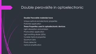
Optoelectronics
Device’s
Name Saqib Ali
Department of Physics
University Of Narowal
Table of contents
� Perovskite Materials
� Double perovskite
� Optoelectronics
� Our purpose or intention
� Future scope
Single Perovskite materials
� Discovered in 1839 by mineralogist , Lev A. Perovski
� Formula ABX3
� Simple cubic close-packed
� Unique physical properties
� Used in optoelectronic and photovoltaic devices
Double Perovskite Materials
� Definition: A compound with a general formula A2BB'O6
� Crystal Structure: Distorted octahedral network
� A2 and BB'O6 sites explained
Advantage of Double Perovskite
� Tunable Properties: Flexibility in choosing A and B elements Enhanced
� Stability: Improved resistance to phase transitions Diverse Electronic
� Properties: Varied electrical and magnetic properties environmental
� Friendliness: Potential for sustainable materials
Applications of Double Perovskite
Materials
� Energy Conversion: Solar cells,
thermoelectric materials
� Catalysis: Oxygen evolution
catalyst
� Data Storage: Magnetic memory
devices
� Superconductors: Potential for
high-temperature
superconductivity
Future Scope
� Emerging Trends: Research and development in double perovskite
materials
� Green Energy: Advancements in solar cells and energy storage
� Quantum Computing: Potential applications in quantum technologies
� Environmental Remediation: Role in pollution control
Optoelectronics Device's
● Optics and Electronics
● Types
● Light into electrical energy
● Electrical energy into light
Examples
� light-emitting diode
� photodiode
� solar cells
� laser diodes
� optical fibre
� photo detector
Historical Perspective
� Emergence of Optoelectronics in the 20th century.
� Development of LEDs (Nick Holonyak Jr., 1962).
� Invention of the Laser (Theodore Maiman, 1960).
� Fiber Optics Revolution (1970s onwards).
Working Principle
� Overview of the working principle:
� Light Emission: LEDs and Lasers.
� Light Detection: Photodiodes and Phototransistors.
� Light Modulation: Liquid Crystal Displays (LCDs).
� Light Amplification: Optical Amplifiers.
Applications
� Overview of diverse
applications:
� Communication: Fiber optics for
high-speed data transmission.
� Display Technology: LEDs, OLEDs,
and LCDs.
� Sensing: Photodetectors for
environmental monitoring.
� Medical Devices: Laser-based
surgeries and diagnostics.
� Energy Efficiency: Solid-state
lighting and solar cells.
.
Advantages of Optoelectronic Devices
� Energy Efficiency: Lower power consumption.
� High Speed: Fast data transmission.
� Compactness: Miniaturized components.
� Durability: Longer lifespan.
� Precision: Accurate sensing and control.
Impact on Latest Technology
� Transformative Role: Enabling
technologies like 5G, autonomous
vehicles, and augmented reality.
� Sustainability: Energy-efficient
lighting and solar energy.
� Healthcare Revolution: Optical
imaging and diagnostics.
� Data Centers: Optical
interconnects for high-speed
data processing.
.
Future Scope
� Emerging Trends: Quantum dot
LEDs, photonic integrated circuits.
� Biomedical Advancements: Non-
invasive diagnostics and
treatment.
� Quantum Communication:
Secure communication via
entangled photons.
� Internet of Things (IoT): Integration
into IoT devices for sensing
and data transfer.
.
Double perovskite in optoelectronic
Double Perovskite materials have
� Unique optical and electronic properties
� Potential application
These Properties used in optoelectronic devices
� Light absorption and emission
� Photovoltaic application
� Light emitting diode (LEDs)
� Tunable Optical properties
� Quantum dots
� Photo detector
� Optical amplification
Purpose or Intention
� To design a material for solar cell
� Efficiency greater than 20 %
� At minimum cost
� Non toxic or eco-friendly
� By the means of DFT
Thank you

Optoelectronics Device’s.pptx

  • 1.
  • 2.
    Table of contents �Perovskite Materials � Double perovskite � Optoelectronics � Our purpose or intention � Future scope
  • 3.
    Single Perovskite materials �Discovered in 1839 by mineralogist , Lev A. Perovski � Formula ABX3 � Simple cubic close-packed � Unique physical properties � Used in optoelectronic and photovoltaic devices
  • 4.
    Double Perovskite Materials �Definition: A compound with a general formula A2BB'O6 � Crystal Structure: Distorted octahedral network � A2 and BB'O6 sites explained
  • 5.
    Advantage of DoublePerovskite � Tunable Properties: Flexibility in choosing A and B elements Enhanced � Stability: Improved resistance to phase transitions Diverse Electronic � Properties: Varied electrical and magnetic properties environmental � Friendliness: Potential for sustainable materials
  • 6.
    Applications of DoublePerovskite Materials � Energy Conversion: Solar cells, thermoelectric materials � Catalysis: Oxygen evolution catalyst � Data Storage: Magnetic memory devices � Superconductors: Potential for high-temperature superconductivity
  • 7.
    Future Scope � EmergingTrends: Research and development in double perovskite materials � Green Energy: Advancements in solar cells and energy storage � Quantum Computing: Potential applications in quantum technologies � Environmental Remediation: Role in pollution control
  • 8.
    Optoelectronics Device's ● Opticsand Electronics ● Types ● Light into electrical energy ● Electrical energy into light Examples � light-emitting diode � photodiode � solar cells � laser diodes � optical fibre � photo detector
  • 9.
    Historical Perspective � Emergenceof Optoelectronics in the 20th century. � Development of LEDs (Nick Holonyak Jr., 1962). � Invention of the Laser (Theodore Maiman, 1960). � Fiber Optics Revolution (1970s onwards).
  • 10.
    Working Principle � Overviewof the working principle: � Light Emission: LEDs and Lasers. � Light Detection: Photodiodes and Phototransistors. � Light Modulation: Liquid Crystal Displays (LCDs). � Light Amplification: Optical Amplifiers.
  • 11.
    Applications � Overview ofdiverse applications: � Communication: Fiber optics for high-speed data transmission. � Display Technology: LEDs, OLEDs, and LCDs. � Sensing: Photodetectors for environmental monitoring. � Medical Devices: Laser-based surgeries and diagnostics. � Energy Efficiency: Solid-state lighting and solar cells. .
  • 12.
    Advantages of OptoelectronicDevices � Energy Efficiency: Lower power consumption. � High Speed: Fast data transmission. � Compactness: Miniaturized components. � Durability: Longer lifespan. � Precision: Accurate sensing and control.
  • 13.
    Impact on LatestTechnology � Transformative Role: Enabling technologies like 5G, autonomous vehicles, and augmented reality. � Sustainability: Energy-efficient lighting and solar energy. � Healthcare Revolution: Optical imaging and diagnostics. � Data Centers: Optical interconnects for high-speed data processing. .
  • 14.
    Future Scope � EmergingTrends: Quantum dot LEDs, photonic integrated circuits. � Biomedical Advancements: Non- invasive diagnostics and treatment. � Quantum Communication: Secure communication via entangled photons. � Internet of Things (IoT): Integration into IoT devices for sensing and data transfer. .
  • 15.
    Double perovskite inoptoelectronic Double Perovskite materials have � Unique optical and electronic properties � Potential application These Properties used in optoelectronic devices � Light absorption and emission � Photovoltaic application � Light emitting diode (LEDs) � Tunable Optical properties � Quantum dots � Photo detector � Optical amplification
  • 16.
    Purpose or Intention �To design a material for solar cell � Efficiency greater than 20 % � At minimum cost � Non toxic or eco-friendly � By the means of DFT
  • 17.