Downloaded 148 times

![Coupling Efficiency
s
F
P
P
soursethefromemittedpower
fibertheintocoupledpower
[5-1]
Source Optical Fiber
sP FP](https://image.slidesharecdn.com/unit-4-170605053820/85/OPTICAL-COMMUNICATION-Unit-4-2-320.jpg)
![Radiance (Brightness) of the source
• B= Optical power radiated from a unit area of the source into a
unit solid angle [watts/(square centimeter per stradian)]](https://image.slidesharecdn.com/unit-4-170605053820/85/OPTICAL-COMMUNICATION-Unit-4-3-320.jpg)
![Surface emitting LEDs have a Lambertian
pattern:
cos),( 0BB [5-2]](https://image.slidesharecdn.com/unit-4-170605053820/85/OPTICAL-COMMUNICATION-Unit-4-4-320.jpg)
![Edge emitting LEDs and laser diodes radiation
pattern
LT
BBB cos
cos
cos
sin
),(
1
0
2
0
2
For edge emitting LEDs, L=1
[5-
3]](https://image.slidesharecdn.com/unit-4-170605053820/85/OPTICAL-COMMUNICATION-Unit-4-5-320.jpg)
![Power Coupled from source to the fiber
rdrdddB
dAdABP
s
r
s
A
sssF
m
f f
max0
0
2
0
2
00
sin),(
),(
[5-4]
sourcetheofangleemissionsolidandarea:and ssA
fiberofangleacceptancesolid
andarea:and ffA ](https://image.slidesharecdn.com/unit-4-170605053820/85/OPTICAL-COMMUNICATION-Unit-4-6-320.jpg)
![Power coupled from LED to the Fiber
rdrdB
rdrdB
rdrddBP
s
r
s
r
s
r
s
s
s
22
00
0
2
0
max0
2
0
0
2
0 0
0
0
NA
sin
sincos2
max0
2
10
222
0
22
stepLED, 2)NA( nBrBrP ss [5-5]](https://image.slidesharecdn.com/unit-4-170605053820/85/OPTICAL-COMMUNICATION-Unit-4-7-320.jpg)
![Power coupling from LED to step-index fiber
• Total optical power from LED:
sincos2
sin),(
2/
0
0
22
0
2
2
0
2/
0
BrdBrP
ddBAP
sss
ss
[5-6]
arP
r
a
arP
P
ss
s
ss
if)NA(
if)NA(
2
2
2
stepLED,
[5-7]](https://image.slidesharecdn.com/unit-4-170605053820/85/OPTICAL-COMMUNICATION-Unit-4-8-320.jpg)
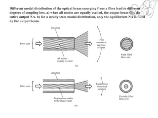
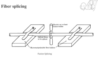
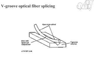
![Fiber-to-Fiber Joint
• Fiber-to-Fiber coupling loss:
• Low loss fiber-fiber joints are either:
1- Splice (permanent bond)
2- Connector (demountable connection)
FFL log10]dB[ [5-8]](https://image.slidesharecdn.com/unit-4-170605053820/85/OPTICAL-COMMUNICATION-Unit-4-12-320.jpg)
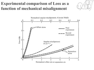
![Mechanical misalignment losses
Lateral (axial) misalignment loss is a dominant
Mechanical loss.
2/12
2step,
2
1
2
arccos
2
a
d
a
d
a
d
a
Acomm
F
[5-9]](https://image.slidesharecdn.com/unit-4-170605053820/85/OPTICAL-COMMUNICATION-Unit-4-14-320.jpg)
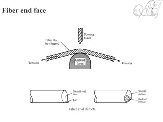
![Longitudinal offset effect
Losses due to differences in the geometry and waveguide characteristics
of the fibers
ER
E
R
F
ER
E
R
F
aL
aa
a
a
aL
NANAfor)
NA
NA
log(20)(
for)log(10)(
[5-10]
E & R subscripts refer to emitting and receiving fibers.](https://image.slidesharecdn.com/unit-4-170605053820/85/OPTICAL-COMMUNICATION-Unit-4-15-320.jpg)
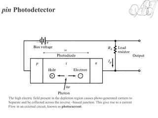
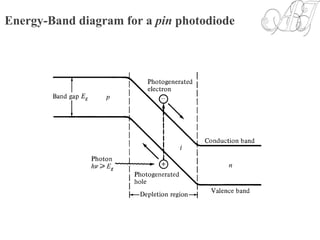
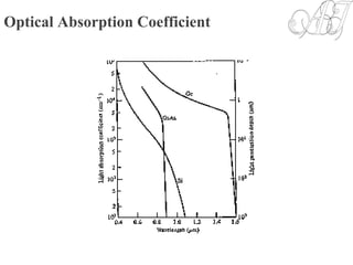
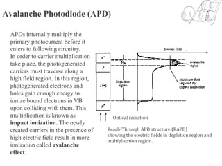
![Photocurrent
• Optical power absorbed, in the depletion region can be written in terms
of incident optical power, :
• Absorption coefficient strongly depends on wavelength. The upper
wavelength cutoff for any semiconductor can be determined by its energy
gap as follows:
• Taking entrance face reflectivity into consideration, the absorbed power in
the width of depletion region, w, becomes:
)1()( )(
0
xs
ePxP
[6-1]
)(s
)(xP
0P
(eV)
24.1
)m(
g
c
E
[6-2]
)1)(1()()1( )(
0 f
w
f RePwPR s
](https://image.slidesharecdn.com/unit-4-170605053820/85/OPTICAL-COMMUNICATION-Unit-4-22-320.jpg)
![Responsivity
• The primary photocurrent resulting from absorption is:
• Quantum Efficiency:
• Responsivity:
)1)(1( )(
0 f
w
p ReP
h
q
I s
[6-3]
hP
qIP
/
/
photonsincidentof#
pairsatedphotogenerhole-electronof#
0
[6-4]
[A/W]
0
h
q
P
I P
[6-5]](https://image.slidesharecdn.com/unit-4-170605053820/85/OPTICAL-COMMUNICATION-Unit-4-24-320.jpg)
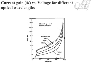
![Responsivity of APD
• The multiplication factor (current gain) M for all carriers generated in the
photodiode is defined as:
• Where is the average value of the total multiplied output current & is
the primary photocurrent.
• The responsivity of APD can be calculated by considering the current gain
as:
p
M
I
I
M [6-6]
MI PI
MM
h
q
0APD
[6-7]](https://image.slidesharecdn.com/unit-4-170605053820/85/OPTICAL-COMMUNICATION-Unit-4-27-320.jpg)
( 0 tmsPtP [6-8]
]currentAC)[(]valueDC[)(ph tiItMP
h
q
i pP
[6-9]
signalsinusoidalfor
2
22
22
2222
P
pp
sps
Im
i
Mii
[6-9]
[6-10]](https://image.slidesharecdn.com/unit-4-170605053820/85/OPTICAL-COMMUNICATION-Unit-4-30-320.jpg)
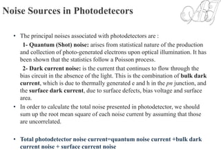
![Noise calculation (1)
• Quantum noise current (lower limit on the sensitivity):
• B: Bandwidth, F(M) is the noise figure and generally is
• Bulk dark current noise:
is bulk dark current
• Surface dark current noise: is the surface current.
)(2 222
MFBMqIi PQQ
0.10)( xMMF x
[6-11]
)(2 222
MFBMqIi DDBDB [6-12]
DI
BqIi LDSDS 222
LI
Note that for pin photodiode
1)(2
MFM
[6-13]](https://image.slidesharecdn.com/unit-4-170605053820/85/OPTICAL-COMMUNICATION-Unit-4-32-320.jpg)
![Noise calculation (2)
• The total rms photodetector noise current is:
• The thermal noise of amplifier connected to the photodetector is:
input resistance of amplifier, and is Boltzmann cte.
BqIMFBMIIq
iiii
LDP
DSDBQNN
2)()(2 2
22222
[6-14]
L
B
TT
R
TBk
i
422
[6-15]
LR -123
JK1038.1
Bk](https://image.slidesharecdn.com/unit-4-170605053820/85/OPTICAL-COMMUNICATION-Unit-4-33-320.jpg)
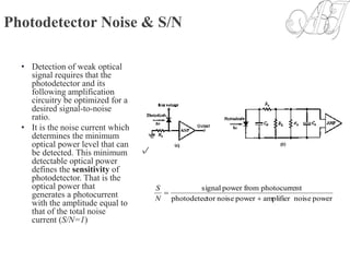
![S/N Calculation
• Having obtained the signal and total noise, the signal-to-noise-ratio can be
written as:
• Since the noise figure F(M) increases with M, there always exists an
optimum value of M that maximizes the S/N. For sinusoidally modulated
signal with m=1 and :
LBLDP
P
RTBkBqIMFBMIIq
Mi
N
S
/42)()(2 2
22
[6-16]
x
MMF )(
)(
/422
opt
DP
LBLx
IIxq
RTkqI
M
[6-17]](https://image.slidesharecdn.com/unit-4-170605053820/85/OPTICAL-COMMUNICATION-Unit-4-34-320.jpg)
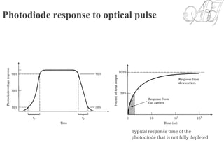
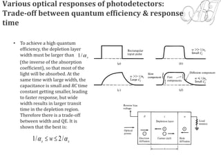
![Photodetector Response Time
• The response time of a photodetector with its output circuit depends mainly
on the following three factors:
1- The transit time of the photocarriers in the depletion region. The transit
time depends on the carrier drift velocity and the depletion layer
width w, and is given by:
2- Diffusion time of photocarriers outside depletion region.
3- RC time constant of the circuit. The circuit after the photodetector acts
like RC low pass filter with a passband given by:
dt dv
d
d
v
w
t [6-18]
TT CR
B
2
1
[6-19]
daTLsT CCCRRR and||](https://image.slidesharecdn.com/unit-4-170605053820/85/OPTICAL-COMMUNICATION-Unit-4-35-320.jpg)


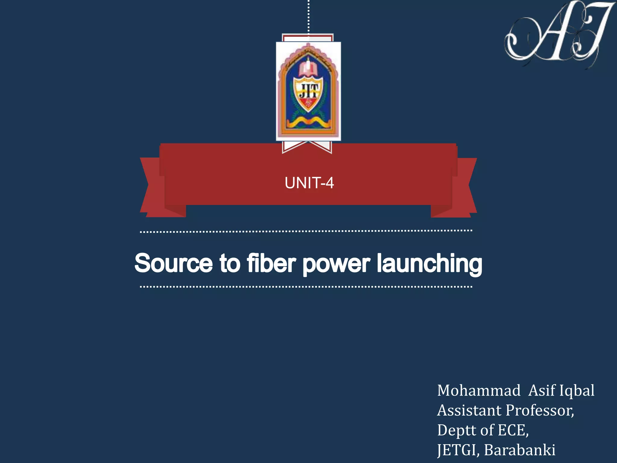
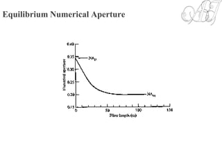
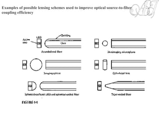
The document discusses optical coupling between light sources and optical fibers. It defines coupling efficiency as the ratio of power coupled into the fiber to power emitted from the source. Radiance and radiation patterns of different light sources are described. Expressions are provided for calculating the power coupled from a source to a fiber based on the source and fiber parameters. Methods to improve coupling efficiency such as lensing are also discussed. The document also covers topics like fiber-to-fiber coupling loss, mechanical misalignment loss, and fiber end defects.