The document discusses different types of photodetectors used to convert optical signals to electrical signals. It compares p-n photodiodes, p-i-n photodiodes, and avalanche photodiodes (APDs). P-i-n photodiodes have a wider depletion region than p-n photodiodes, allowing them to operate at longer wavelengths. APDs have additional gain from impact ionization, multiplying the number of carriers generated. However, APDs require high reverse bias voltages, have additional noise, and gain varies with temperature. The response time of APDs can also be limited compared to p-i-n photodiodes due to the avalanche multiplication process.
Chapter introduction to optical detectors focusing on the conversion of optical signals to electrical signals.
Essential characteristics needed for detectors, such as high sensitivity, fidelity, low noise, and reliability.
Overview of p-n photodiode operation, focusing on carrier movement and the photogeneration process.
Explanation of diffusion versus drift current in photodiodes, and factors affecting response time and capacitance.Deep dive into response time calculations and effects of capacitance and resistance on photodetector speed.
Classification of semiconductor photodiodes into those with or without internal gain and their operational principles.Description of APD structure and operational principles, including impact ionization and carrier multiplication.
Discussion of drawbacks of APDs such as fabrication complexity, noise, and operational voltage requirements.
Definition and significance of the multiplication factor in APDs regarding output current and gain.
Comparison of performance metrics between PIN and APD photodiodes across various parameters.
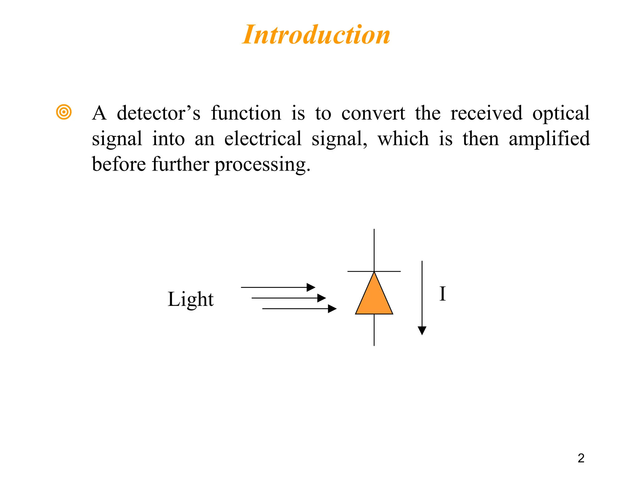
Introduction
A detector’sfunction is to convert the received optical
signal into an electrical signal, which is then amplified
before further processing.
2
I
Light
3.
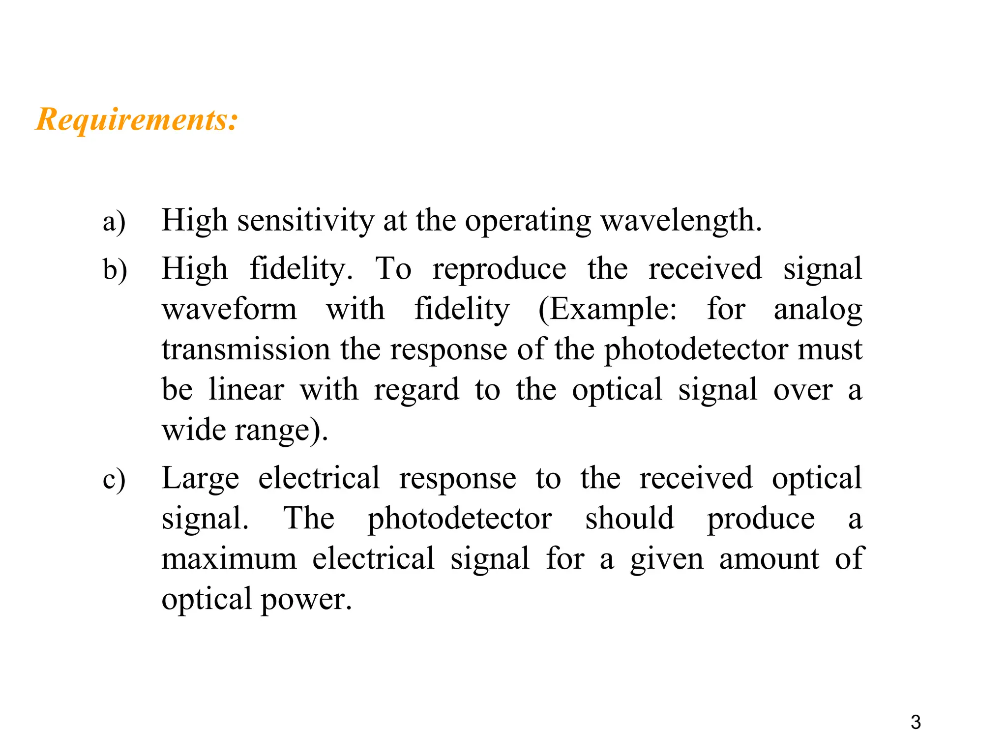
a) High sensitivityat the operating wavelength.
b) High fidelity. To reproduce the received signal
waveform with fidelity (Example: for analog
transmission the response of the photodetector must
be linear with regard to the optical signal over a
wide range).
c) Large electrical response to the received optical
signal. The photodetector should produce a
maximum electrical signal for a given amount of
optical power.
3
Requirements:
4.
4
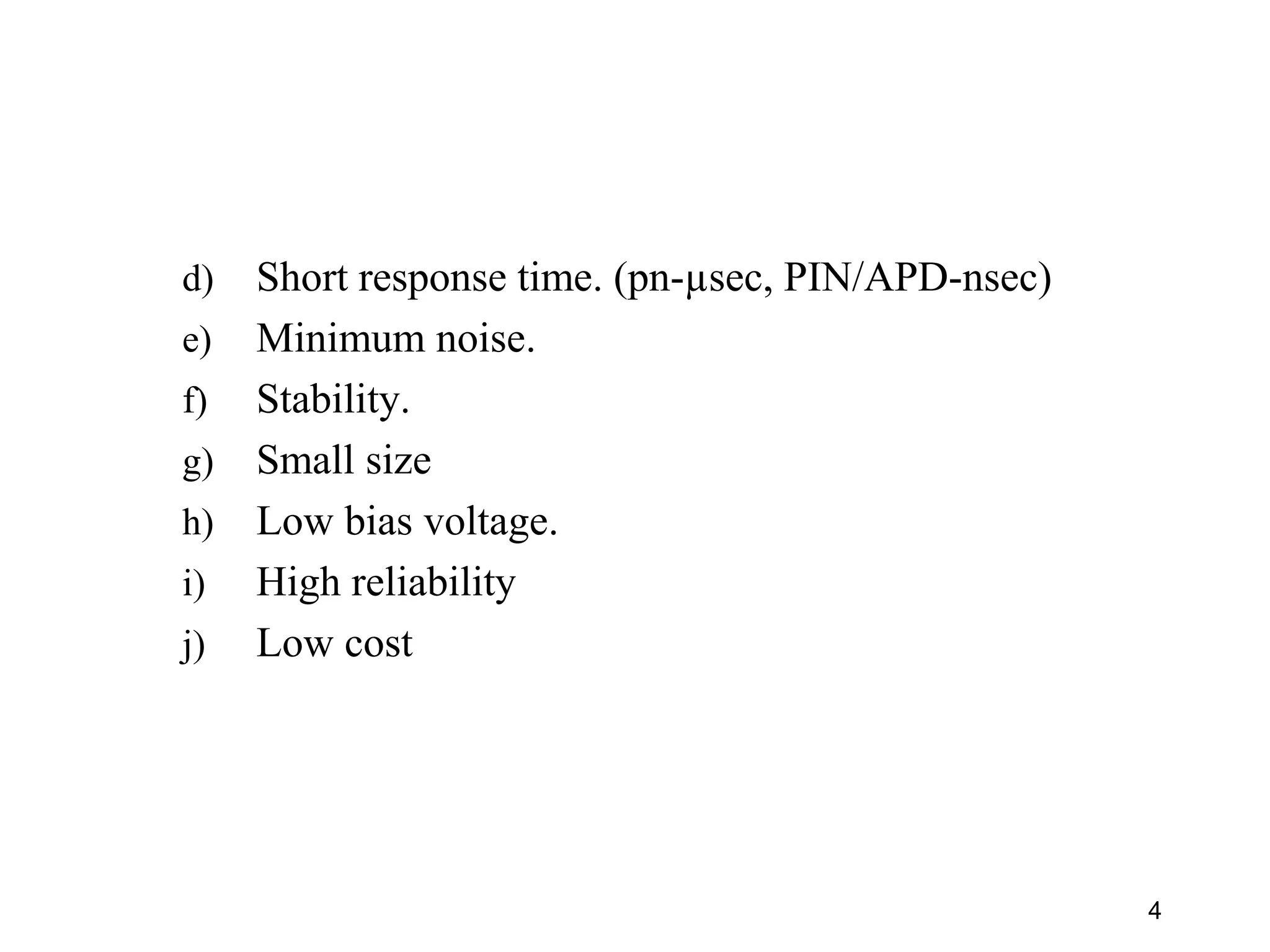
d) Short responsetime. (pn-µsec, PIN/APD-nsec)
e) Minimum noise.
f) Stability.
g) Small size
h) Low bias voltage.
i) High reliability
j) Low cost
5.
Optical Detection Principles
5
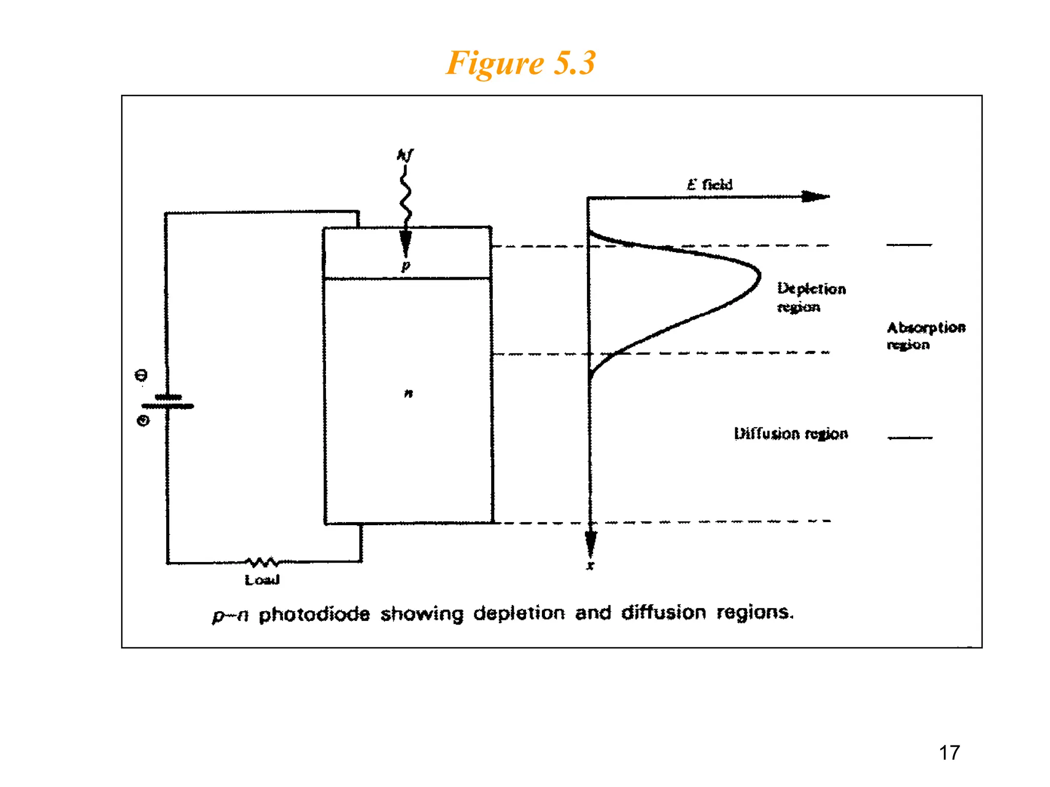
Operationof the p-n photodiode: (a) the structure of the reverse biased p-n junction
illustrating carrier drift in the depletion region; (b) the energy band diagram of the reverse
biased p-n junction showing photogeneration and the subsequent separation of an electron-
hole pair.
Fig. 5.1
(a)
(b)
6.
This deviceis reverse biased and the electric field develop across the
p-n junction sweeps mobile carriers (holes and electrons) to their
respective majority sides (p and n).
A photon incident in or near the depletion region of this device
which has an energy greater than or equal to the bandgap energy Eg
of the fabricating material (i.e. hf > Eg) will excite an electron from
the valence band into the conduction band.
This process leaves an empty hole in the valance band and is known
as the photogeneration of an electron-hole (carrier) pair.
6
7.
7
Carriers pairsso generated near the junction are separated and swept
(drift) under the influence of the electric field to produce a
displacement current in the external circuit in excess of any reverse
leakage current (Fig 5.1 (a)).
Photogeneration and the separation of a carrier pair in the depletion
region of this reverse biased p-n junction is illustrated in Fig. 5.1 (b).
8.
8
Absorption outsidedepletion region – diffusion
current - reduces speed.
Absorption inside depletion region – drift current –
fast due to the large electrical field.
The depletion region must be sufficiently thick to allow a large
fraction of the incident light to be absorbed in order to achieve
maximum carrier pair generation. (PN 1 to 3µm, PIN 20 to 50µm).
However, since long carrier drift times in the depletion region restrict
the speed of operation of the photodiode it is necessary to limit its
width.
9.
9
Photodetector Characteristics
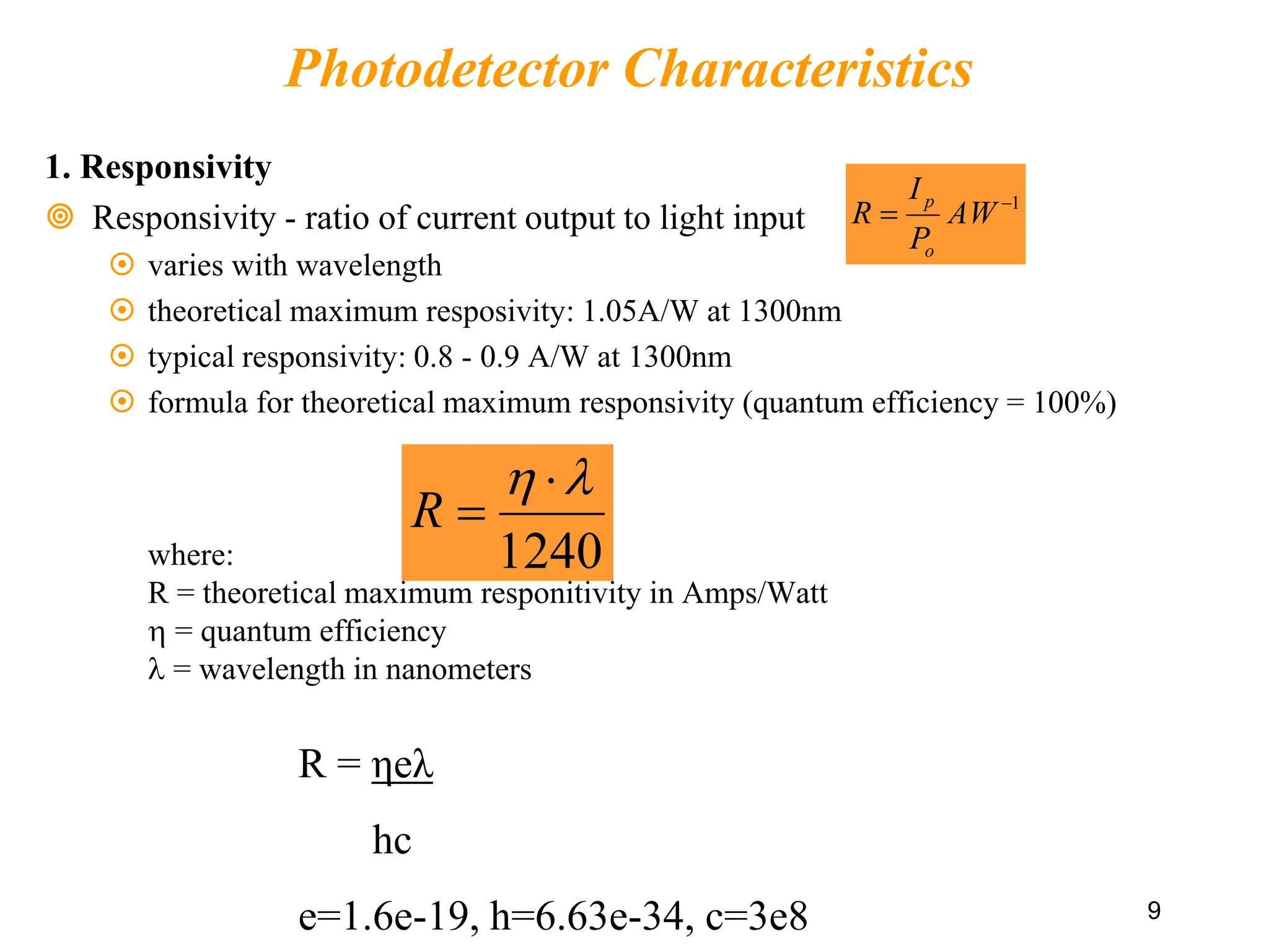
1. Responsivity
Responsivity - ratio of current output to light input
varies with wavelength
theoretical maximum resposivity: 1.05A/W at 1300nm
typical responsivity: 0.8 - 0.9 A/W at 1300nm
formula for theoretical maximum responsivity (quantum efficiency = 100%)
where:
R = theoretical maximum responitivity in Amps/Watt
= quantum efficiency
= wavelength in nanometers
1240
R
R = ηeλ
hc
e=1.6e-19, h=6.63e-34, c=3e8
1
AW
P
I
R
o
p
10.
10
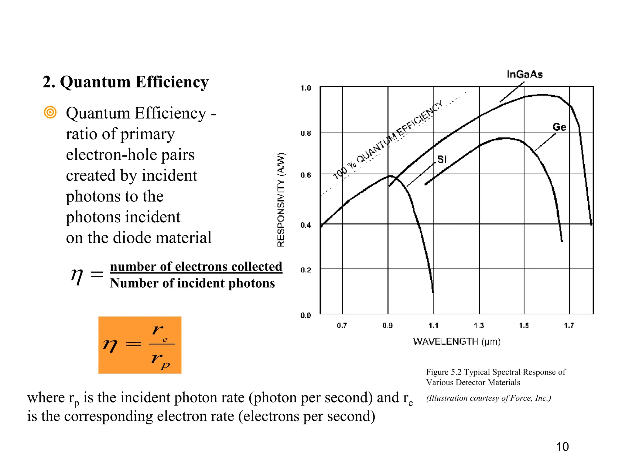
Quantum Efficiency-
ratio of primary
electron-hole pairs
created by incident
photons to the
photons incident
on the diode material
Figure 5.2 Typical Spectral Response of
Various Detector Materials
(Illustration courtesy of Force, Inc.)
2. Quantum Efficiency
p
r
re
number of electrons collected
Number of incident photons
where rp is the incident photon rate (photon per second) and re
is the corresponding electron rate (electrons per second)
11.
11
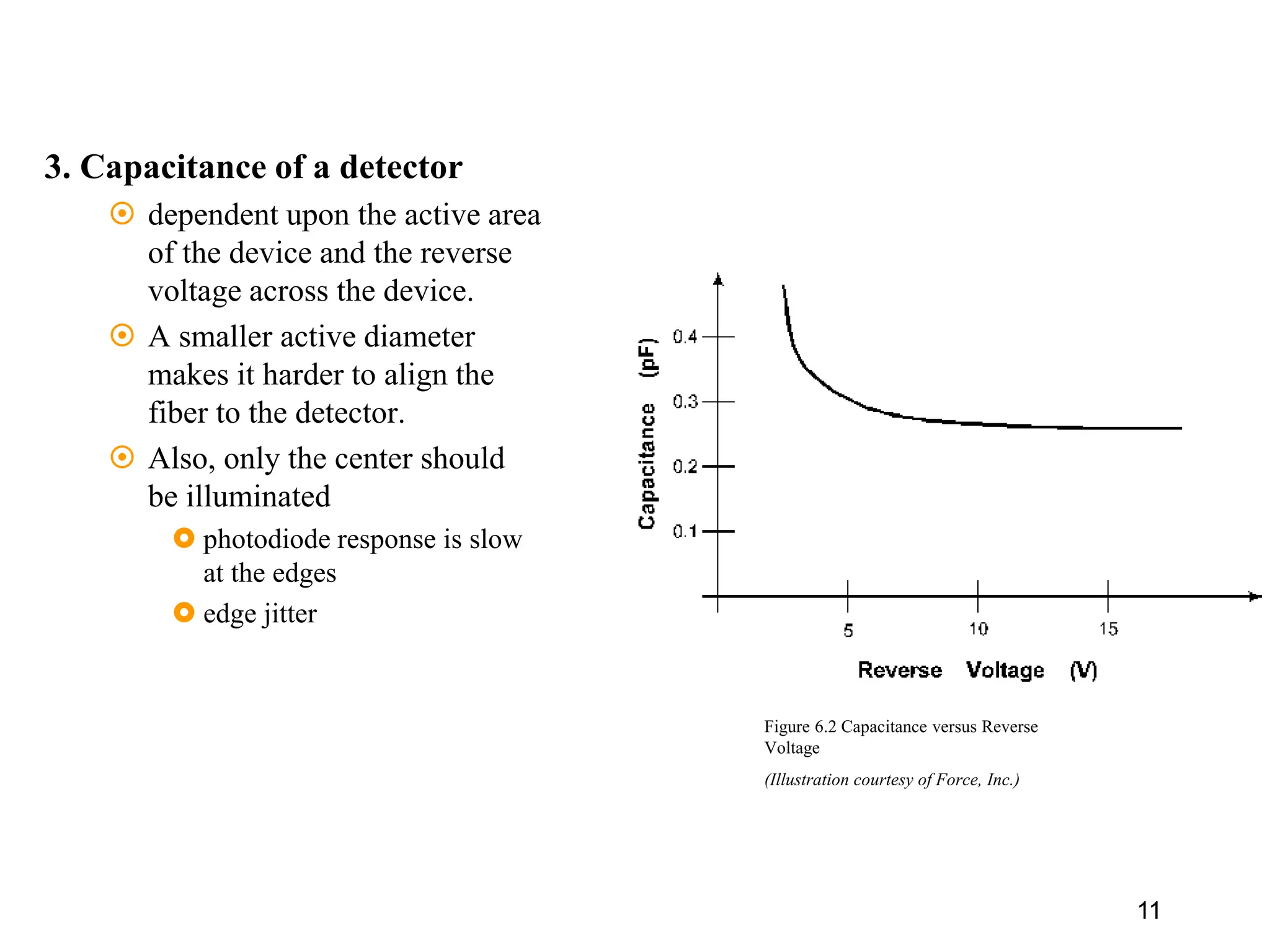
3. Capacitance ofa detector
dependent upon the active area
of the device and the reverse
voltage across the device.
A smaller active diameter
makes it harder to align the
fiber to the detector.
Also, only the center should
be illuminated
photodiode response is slow
at the edges
edge jitter
Figure 6.2 Capacitance versus Reverse
Voltage
(Illustration courtesy of Force, Inc.)
12.
12
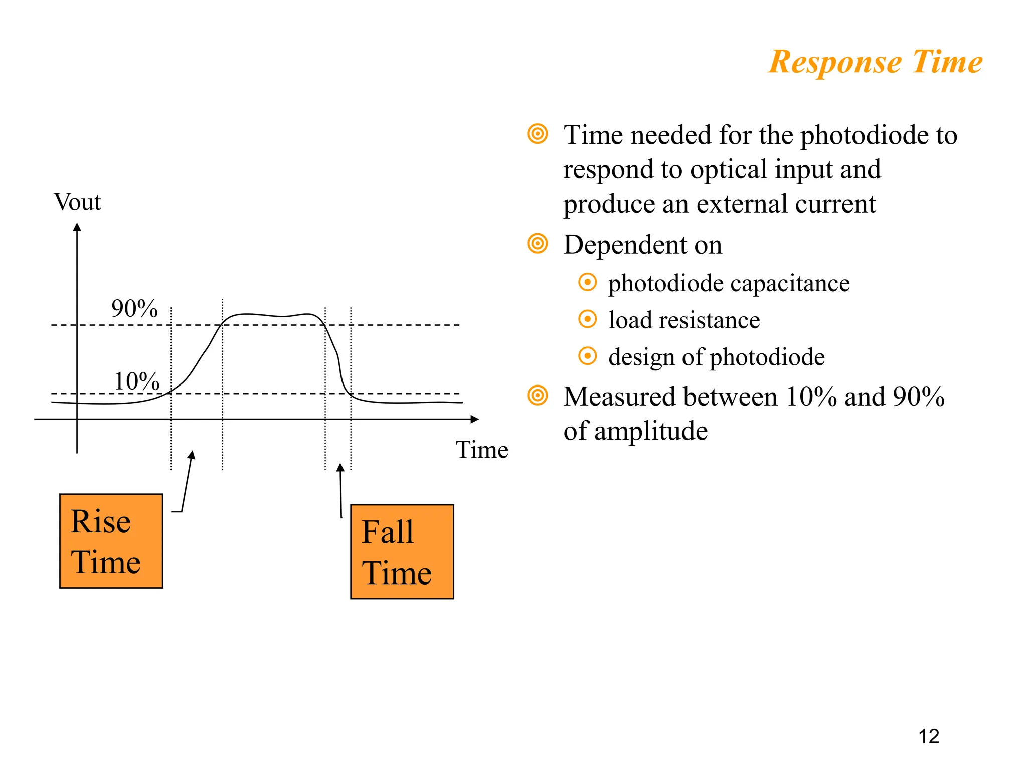
Response Time
Timeneeded for the photodiode to
respond to optical input and
produce an external current
Dependent on
photodiode capacitance
load resistance
design of photodiode
Measured between 10% and 90%
of amplitude
90%
10%
Vout
Time
Rise
Time
Fall
Time
13.
13
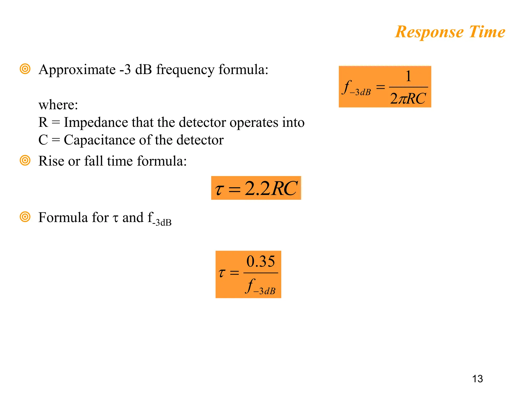
Response Time
Approximate-3 dB frequency formula:
where:
R = Impedance that the detector operates into
C = Capacitance of the detector
Rise or fall time formula:
Formula for and f-3dB
RC
f dB
2
1
3
RC
2
.
2
dB
f 3
35
.
0
14.
14
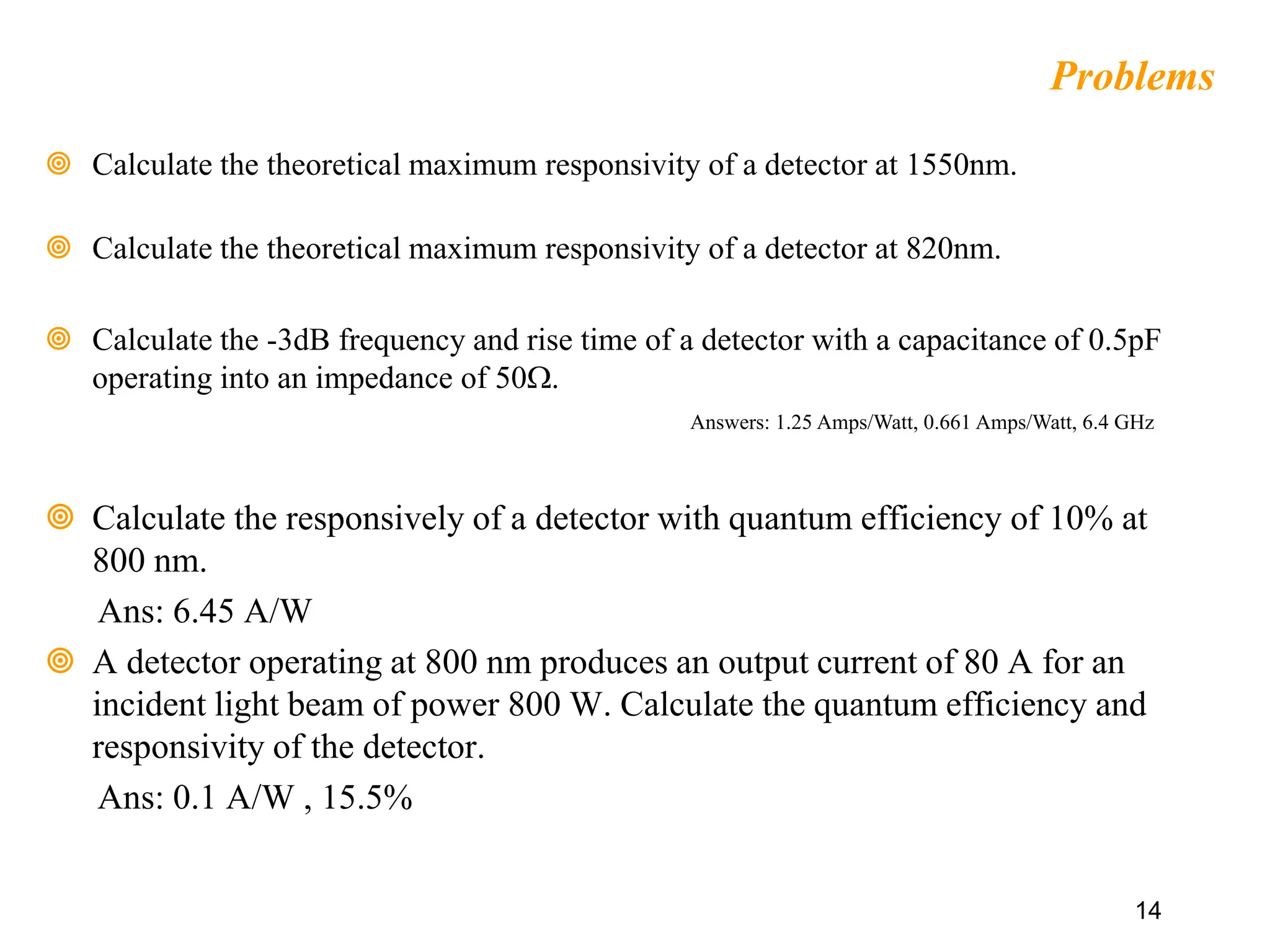
Problems
Calculate thetheoretical maximum responsivity of a detector at 1550nm.
Calculate the theoretical maximum responsivity of a detector at 820nm.
Calculate the -3dB frequency and rise time of a detector with a capacitance of 0.5pF
operating into an impedance of 50W.
Calculate the responsively of a detector with quantum efficiency of 10% at
800 nm.
Ans: 6.45 A/W
A detector operating at 800 nm produces an output current of 80 A for an
incident light beam of power 800 W. Calculate the quantum efficiency and
responsivity of the detector.
Ans: 0.1 A/W , 15.5%
Answers: 1.25 Amps/Watt, 0.661 Amps/Watt, 6.4 GHz
15.
Semiconductor diodescan be classified
into two categories
1. With internal gain
2. Without internal gain
Semiconductor photodiodes without
internal gain generate a single electron
hole pair per absorbed photon.
15
Semiconductor Photodiodes
16.
Semiconductor Photodiodes WithoutInternal Gain
a) P-N Photodiode as given in figure 5.3
16
In the depletion region the carrier pairs separate and drift under
the influence of the electric field, whereas outside this region
the hole diffuses towards the depletion region in order to be
collected .
The diffusion process is very slow compared to the drift process
and thus limits the response of the photodiode.
18
It is thereforeimportant that the photons are absorbed in the
depletion region.
Thus it is made as long as possible by decreasing the doping in
the n type material.
The depletion region width in a p-n photodiode is normally 1-
3µm and is optimized for the efficient detection of light at a
given wavelength.
19.
19
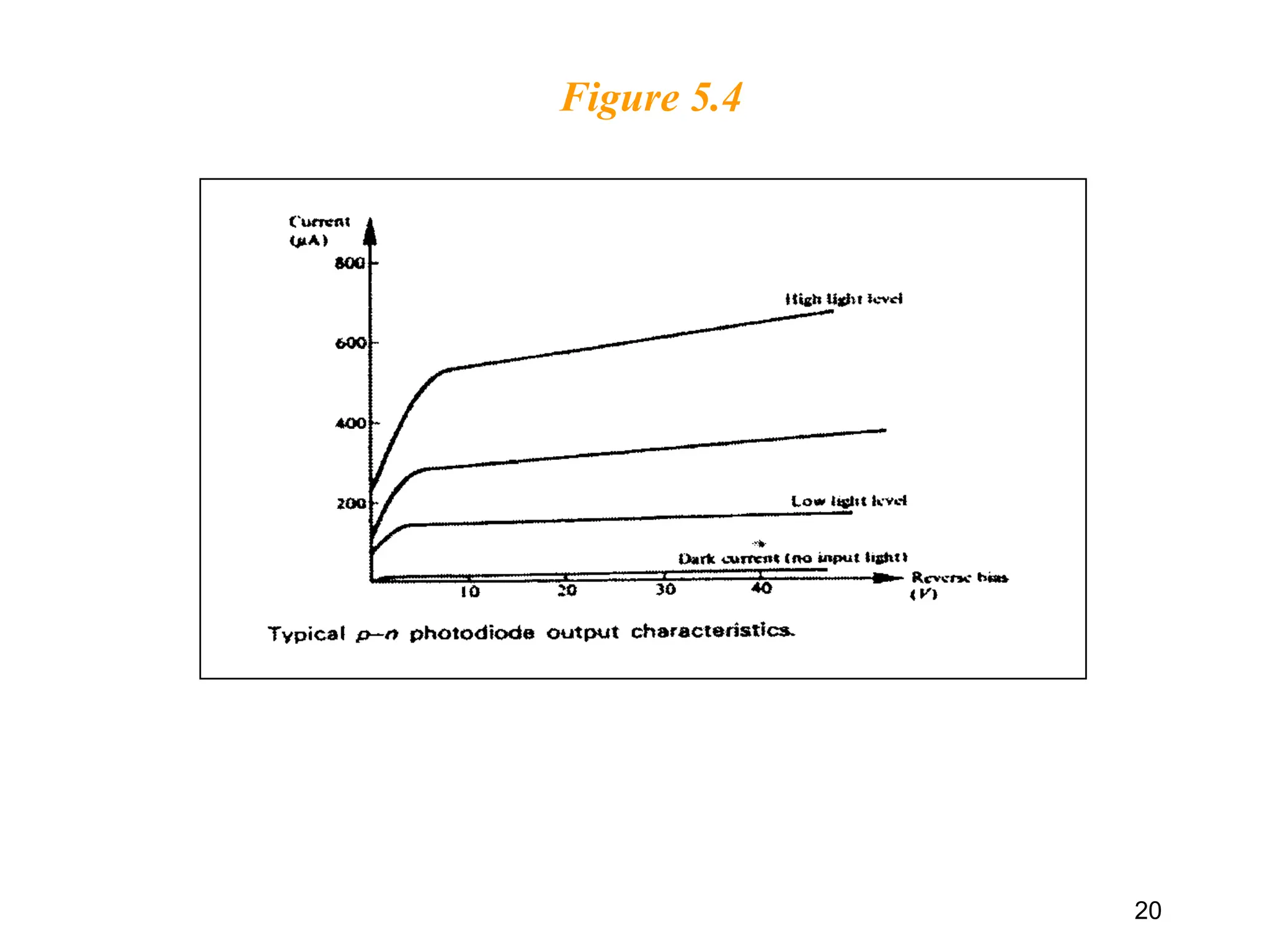
Typical output characteristicsfor the reverse-biased p-n
photodiode is illustrate in Fig 5.4.
The different operating conditions may be noted moving from no
light input to a high light level.
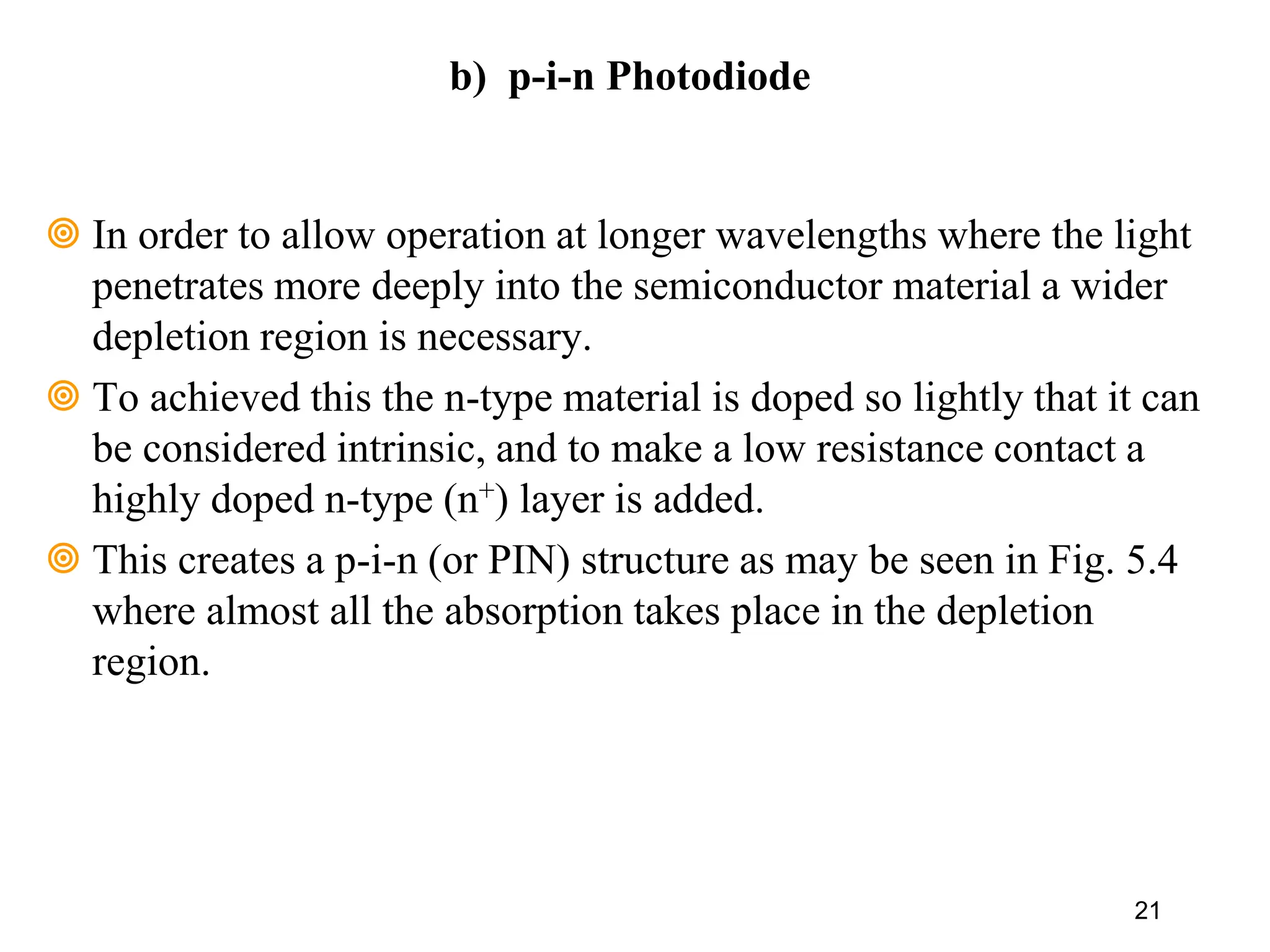
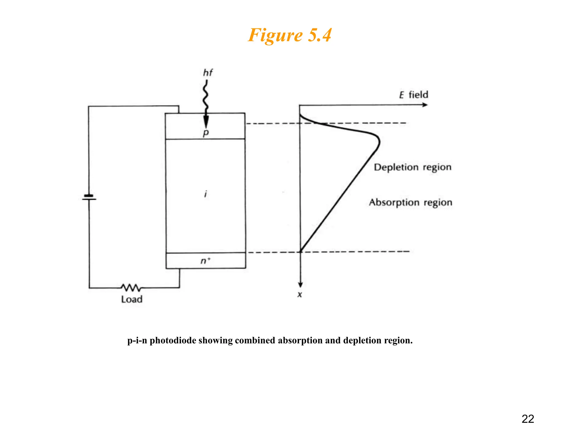
In orderto allow operation at longer wavelengths where the light
penetrates more deeply into the semiconductor material a wider
depletion region is necessary.
To achieved this the n-type material is doped so lightly that it can
be considered intrinsic, and to make a low resistance contact a
highly doped n-type (n+) layer is added.
This creates a p-i-n (or PIN) structure as may be seen in Fig. 5.4
where almost all the absorption takes place in the depletion
region.
21
b) p-i-n Photodiode
23
Germanium p-i-nphotodiodes which span the entire wavelength
range of interest are also commercially available, but the dark
current is relatively high.
Dark current arises from surface leakage currents as well as generation-
recombination currents in the depletion region in the absence of illumination.
24.
Semiconductor Photodiode withInternal Gain -
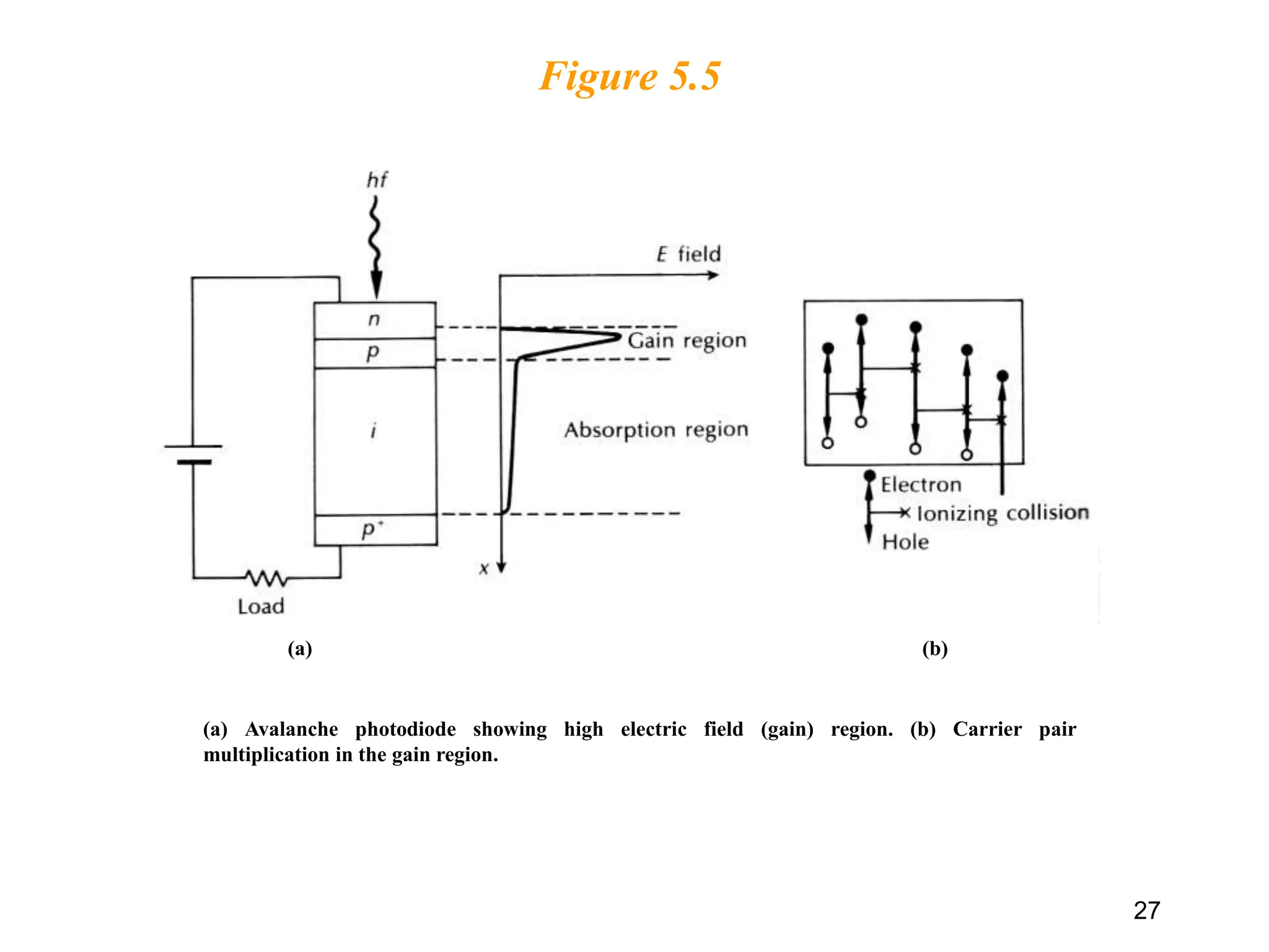
Avalanche Photodiode (APD)
The APD has more sophisticated structure than the p-i-n
photodiode in order to create an extremely high electric field
region.
Therefore, as well as the depletion region where most of the
photons are absorbed and the primary carrier pairs generated
there is a high field region in which holes and electrons can
acquire sufficient energy to excite new electron-hole pairs.
The process is known as impact ionization and is the
phenomenon that leads to avalanche breakdown.
24
25.
25
It requiresvery high reverse bias voltage (100-400 V) in order
that the new carriers created by impact ionization can themselves
produce additional carriers by the same mechanism as shown in
Fig. 5.5 (b).
Carrier multiplication factors as great as 105 may be obtained
using defect free materials to ensure uniformity of carrier
multiplication over the entire photosensitive area.
26.
26
High reversevoltage. This accelerates electrons and holes
thereupon acquires high energy. They strike neutral atoms
and generates more free charge carriers. These secondary
charges then ionize other carriers.
Primary generated electrons strike bonded electrons at the
VB and excite them to the CB. Known as Impact
Ionization.
The main advantage compared to p-i-n photodiode is the
multiplication or gain factor, M.
27.
Figure 5.5
27
(a) (b)
(a)Avalanche photodiode showing high electric field (gain) region. (b) Carrier pair
multiplication in the gain region.
28.
28
Often anasymmetric pulse shape is obtained from the APD
which results from a relatively fast rise time as the electrons are
collected and a fall time dictated by the transit time of the holes
travelling at a slower speed.
Hence, although the use of suitable materials and structures may
gives rise times between 150 and 200 ps, fall times of a 1 ns or
more are quite common which limit the overall response of the
device.
29.
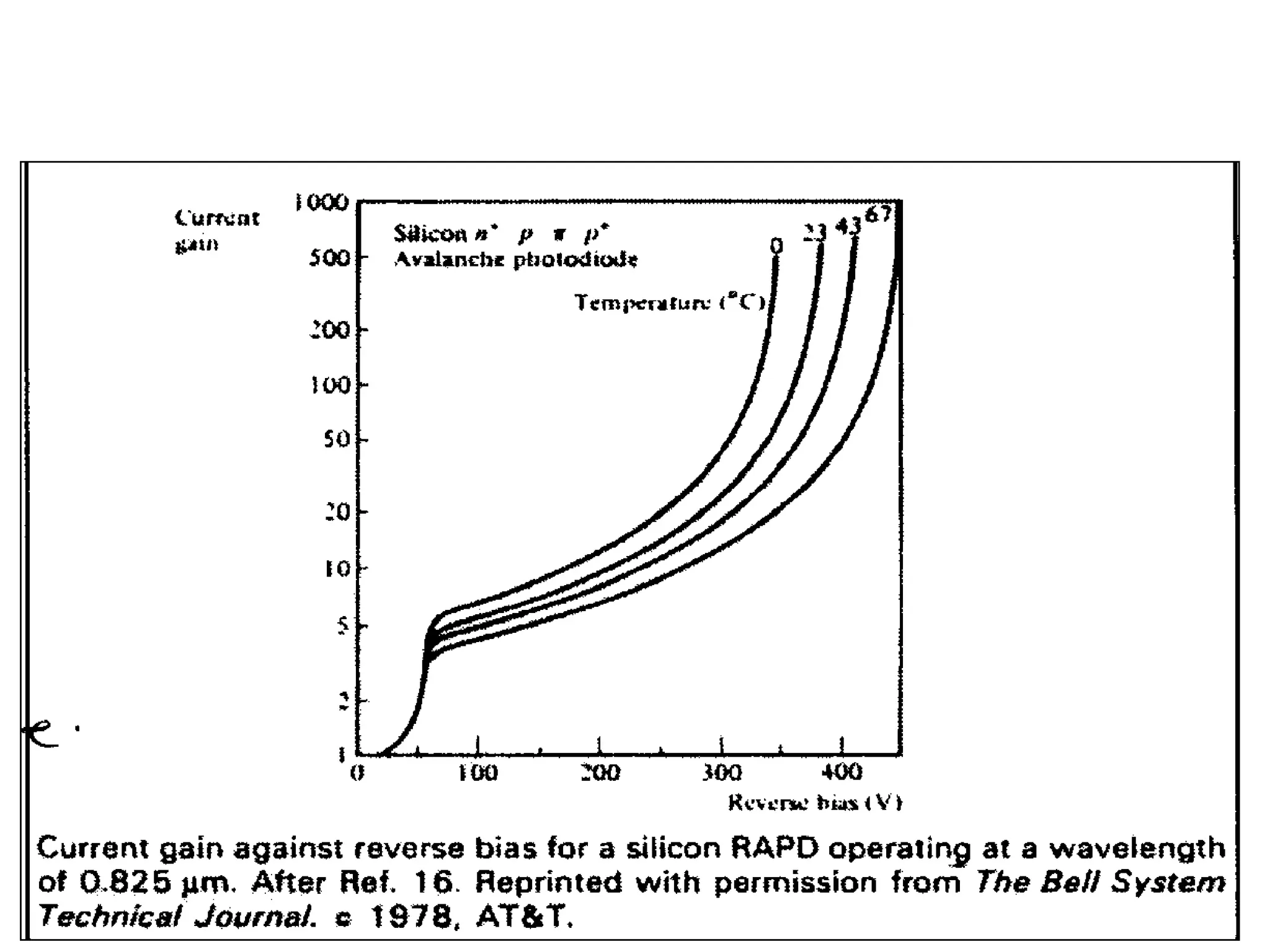
Drawbacks of TheAvalanche Photodiode
1. Fabrication difficulties due to their more complex structure and
hence increased cost.
2. The random nature of the gain mechanism which gives an
additional noise contribution.
3. The high bias voltages required (100-400 V).
4. The variation of the gain with temperature.
29
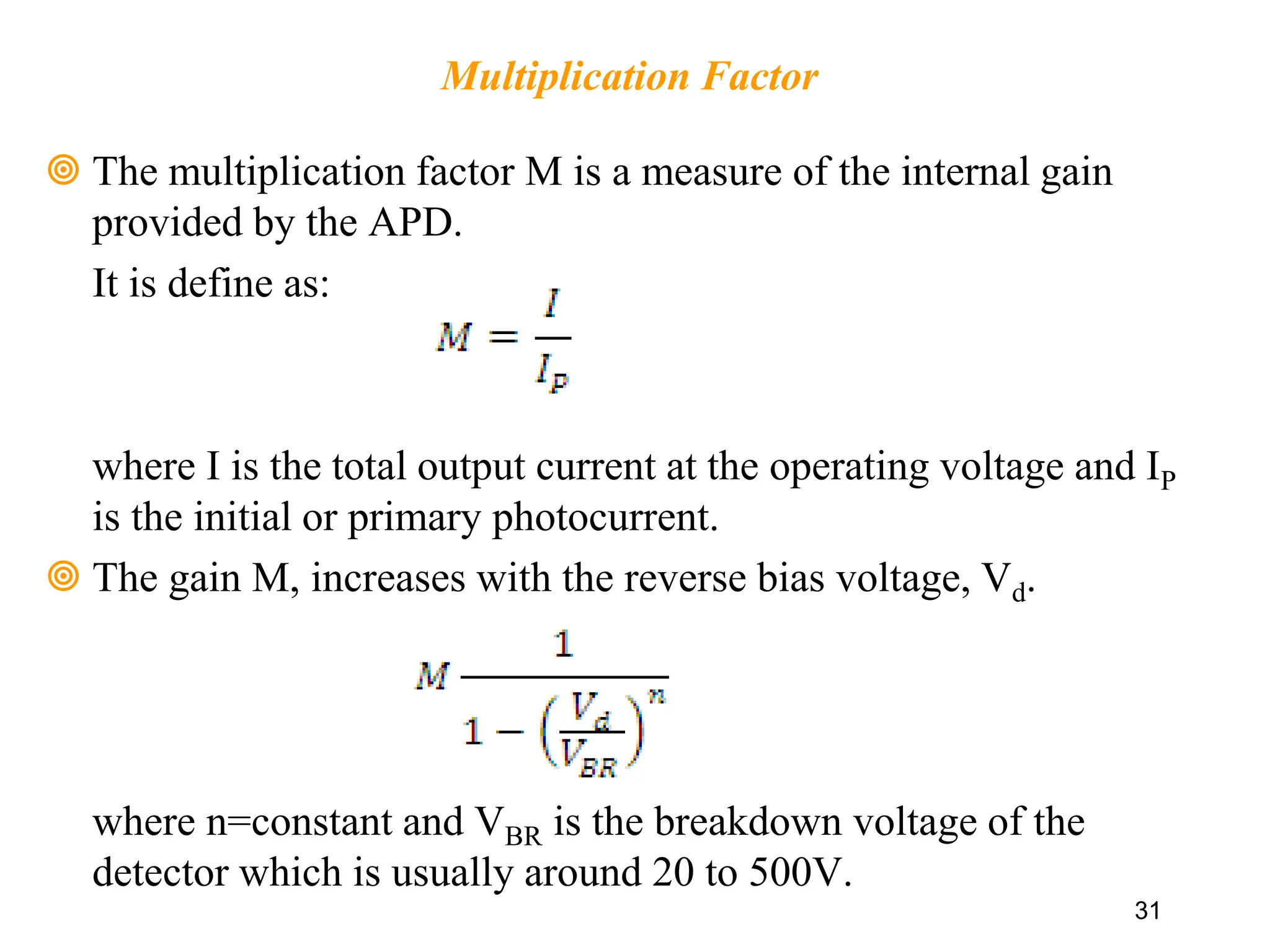
Multiplication Factor
Themultiplication factor M is a measure of the internal gain
provided by the APD.
It is define as:
where I is the total output current at the operating voltage and IP
is the initial or primary photocurrent.
The gain M, increases with the reverse bias voltage, Vd.
where n=constant and VBR is the breakdown voltage of the
detector which is usually around 20 to 500V.
31
32.
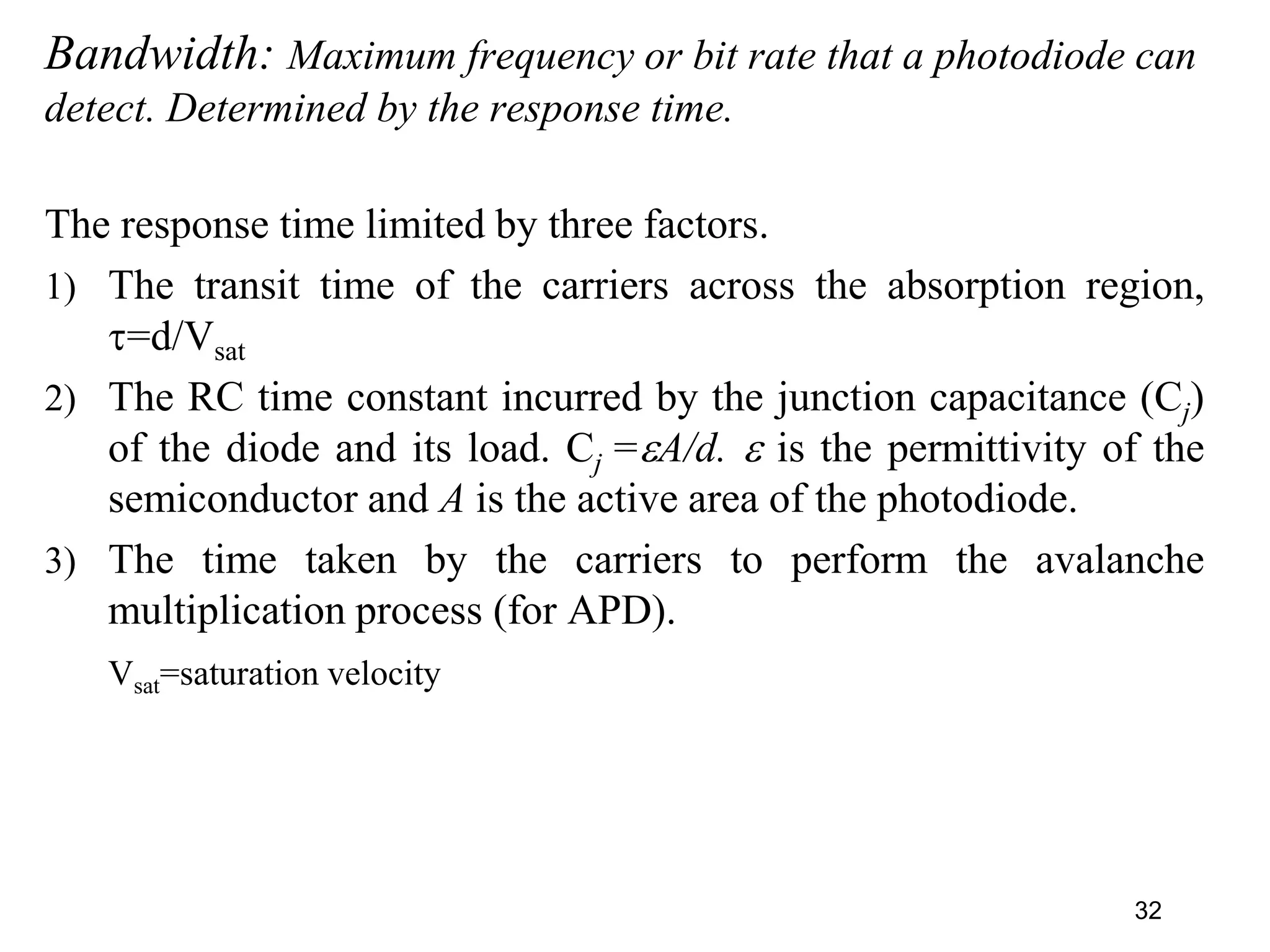
Bandwidth: Maximum frequencyor bit rate that a photodiode can
detect. Determined by the response time.
The response time limited by three factors.
1) The transit time of the carriers across the absorption region,
=d/Vsat
2) The RC time constant incurred by the junction capacitance (Cj)
of the diode and its load. Cj =A/d. is the permittivity of the
semiconductor and A is the active area of the photodiode.
3) The time taken by the carriers to perform the avalanche
multiplication process (for APD).
Vsat=saturation velocity
32
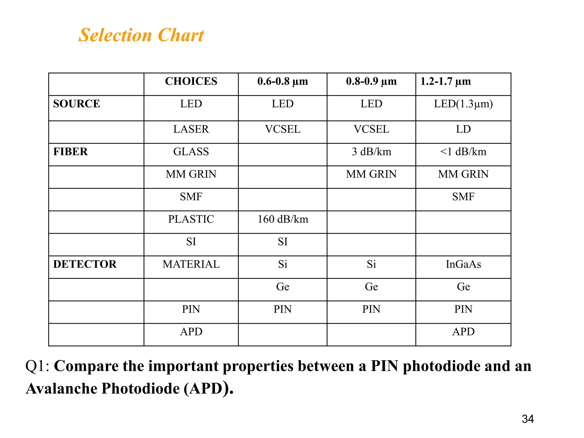
Selection Chart
34
CHOICES 0.6-0.8µm 0.8-0.9 µm 1.2-1.7 µm
SOURCE LED LED LED LED(1.3µm)
LASER VCSEL VCSEL LD
FIBER GLASS 3 dB/km <1 dB/km
MM GRIN MM GRIN MM GRIN
SMF SMF
PLASTIC 160 dB/km
SI SI
DETECTOR MATERIAL Si Si InGaAs
Ge Ge Ge
PIN PIN PIN PIN
APD APD
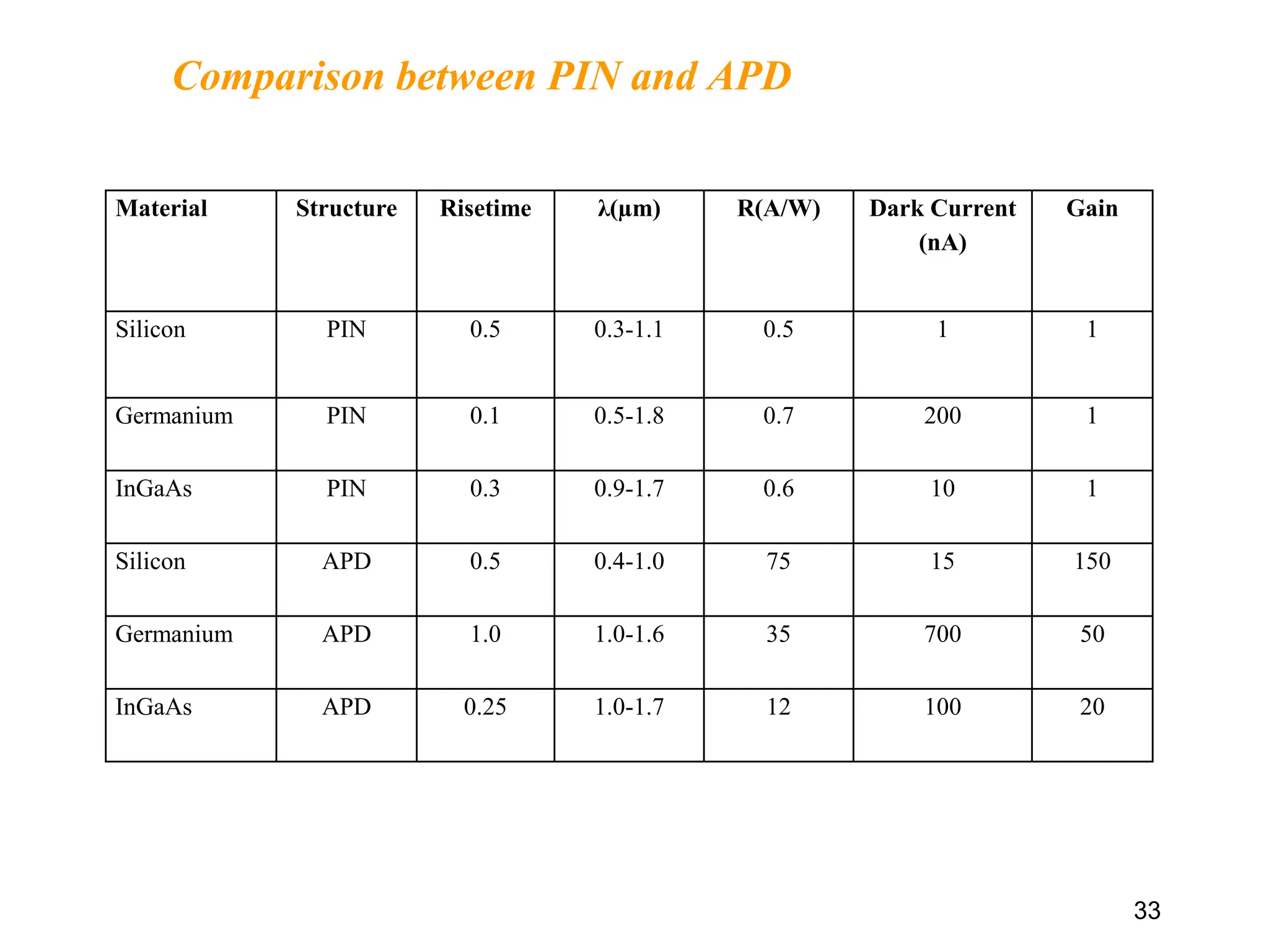
Q1: Compare the important properties between a PIN photodiode and an
Avalanche Photodiode (APD).