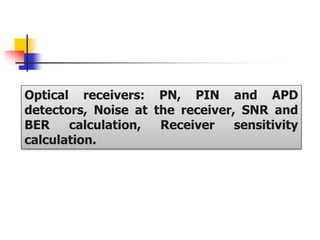
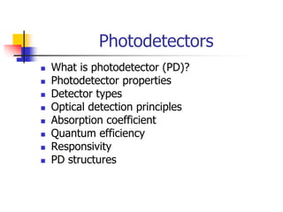
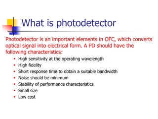
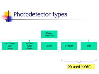
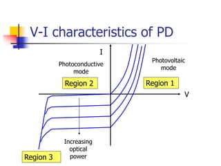
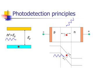
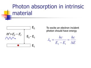
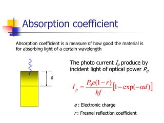
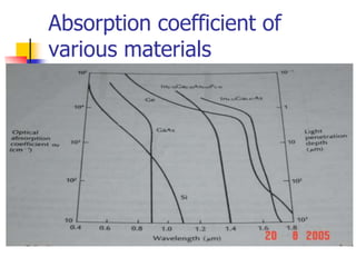
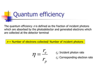
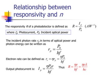
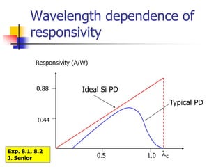
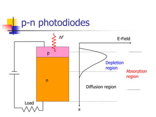
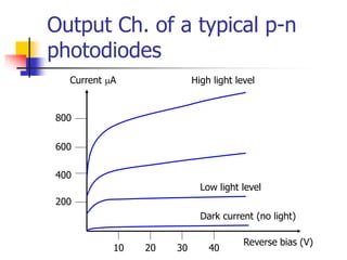
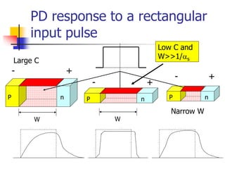
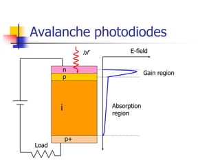
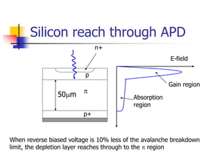
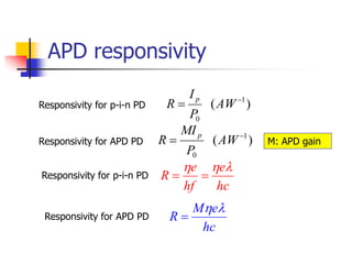
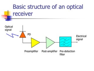
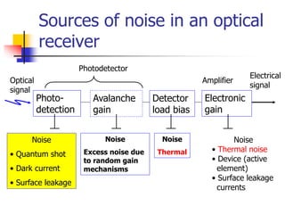
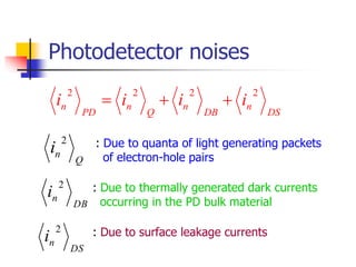
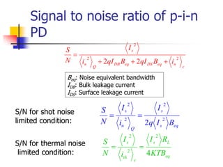
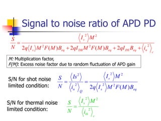
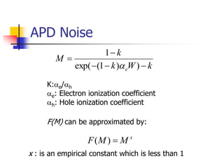
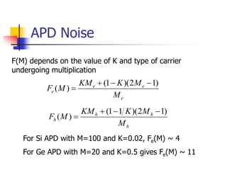
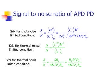
Course Code: EEE 409
Course Title: Optical Fiber Communication
Department of Electrical and Electronic Engineering
Hajee Mohammad Danesh
Science and Technology University, Dinajpur-5200
Course Teacher
Md. Sazedur Rahman
Lecturer
Dept. of Electrical and Electronic Engineering (EEE)
Hajee Mohammad Danesh Science and Technology University (HSTU)
Optical receivers: PN, PIN and APD
detectors, Noise at the receiver, SNR and
BER calculation, Receiver sensitivity
calculation.
Photodetectors
 What is photodetector (PD)?
 Photodetector properties
 Detector types
 Optical detection principles
 Absorption coefficient
 Quantum efficiency
 Responsivity
 PD structures
What is photodetector
Photodetector is an important elements in OFC, which converts
optical signal into electrical form. A PD should have the
following characteristics:
 High sensitivity at the operating wavelength
 High fidelity
 Short response time to obtain a suitable bandwidth
 Noise should be minimum
 Stability of performance characteristics
 Small size
 Low cost
Photodetector types
Photo-
detectors
Photomulti-
plier
tubes
Vacuum
Photo-
diodes
pn-PD P-i-N PD APD
PD used in OFC
V-I characteristics of PD
I
V
Region 2 Region 1
Region 3
Increasing
optical
power
Photovoltaic
mode
Photoconductive
mode
Photodetection principles
Eg
hf >Eg
- +
p n
Photon absorption in intrinsic
material
E2 - E1
hf >E2 – E1
E2
E1
To excite an electron incident
photon should have energy
E
hc
E
E
hc




1
2
0

Absorption coefficient
Absorption coefficient is a measure of how good the material is
for absorbing light of a certain wavelength
d
 
)
exp(
1
)
1
(
0
d
hf
r
e
P
Ip 




The photo current Ip produce by
incident light of optical power P0
e : Electronic charge
r : Fresnel reflection coefficient
Absorption coefficient of
various materials
Quantum efficiency
The quantum efficiency n is defined as the fraction of incident photons
which are absorbed by the photodetector and generated electrons which
are collected at the detector terminal
p
e
r
r


n = Number of electrons collected/ Number of incident photons
rp: Incident photon rate
re: Corresponding electron rate
Relationship between
responsivity and n
hf
P
r
r p
e
0

 

)
( 1
0

 AW
P
I
R
p
hf
P
rp
0

where Ip: Photocurrent, P0: Incident optical power
The incident photon rate rp in terms of optical power and
photon energy can be written as
The responsivity R of a photodetector is defined as
Electron rate can be defined as
Output photocurrent is:
hf
e
P
Ip
0

 Thus
hc
e
hf
e
R





Wavelength dependence of
responsivity
Responsivity (A/W)
0.44
0.88
0.5 1.0 c
Ideal Si PD
Typical PD
Exp. 8.1, 8.2
J. Senior
p-n photodiodes
E-Field
Depletion
region
Absorption
region
hf
x
p
n
Diffusion region
Load
Output Ch. of a typical p-n
photodiodes
Reverse bias (V)
Current A
10 20 30 40
200
400
600
800
High light level
Low light level
Dark current (no light)
p-i-n Photodiode
E-Field
Depletion region
Absorption region
hf
x
p
i
Load
n
p-i-n photodiode structures
Metal contact
SiO2
Antireflection
coating
Depletion layer
P+
n+
hf
Front illuminated Si PD
i
Metal contact
n+
p+
i
Antireflection
coating
Reflection
coating
Side illuminated Si PD
Speed of response of PD
There are three main factors that limit the
speed of response of a PD
 Drift time of carrier (depletion region)
 Diffusion time of carriers (outside of
depletion region)
 Transition capacitance
Speed of response of PD
Drift time of carriers through the depletion region:
d
drift
v
w
t 
w : width of depletion region
vd : drift velocity
For electric field 2x10⁴ v/cm, vd=107cm/s,
tdrift=0.1 ns when w=10 micron
Diffusion time of carriers outside the depletion region:
c
difft
D
d
t
2
2

d : carriers diffusion distance
Dc : diffusion coefficient
For 10 m diffusion distance, hole
diffusion time 40 ns whereas electron
diffusion time is only 8 ns
Speed of response of PD
Time constant incurred by the capacitance of the PD with its load:
w
A
Cj


To maximize the speed of response, the transit time need to minimize by
Increasing bias voltage
Decreasing layer thickness
Increasing bias voltage resulting to increase drift speed, which lead to
reduce drift time. Further depletion layer thickness may increase with
bias voltage
Quantum efficiency will fall with decreasing layer thickness, w. It also
increase junction capacitance, which lead to rise RC time constant. Thus
device speed will slowdown
PD response to a rectangular
input pulse
W W
P n n n
P P
+
- +
+
-
-
Large C
Narrow W
Low C and
W>>1/s
Avalanche photodiodes
hf
Load
n
p
p+
i
Gain region
Absorption
region
E-field
Silicon reach through APD
p+
p

n+
50m Absorption
region
Gain region
E-field
When reverse biased voltage is 10% less of the avalanche breakdown
limit, the depletion layer reaches through to the  region
APD response time
APD response time is limited by:
 Transit time of the carrier across the
absorption region
 Time taken for avalanche multiplication
 RC time constant
APD responsivity
hc
e
hf
e
R





)
( 1
0

 AW
P
I
R
p
Responsivity for p-i-n PD
Responsivity for APD PD )
( 1
0

 AW
P
MI
R
p
M: APD gain
Responsivity for p-i-n PD
hc
e
M
R



Responsivity for APD PD
Basic structure of an optical
receiver
PD
Preamplifier Post-amplifier Pre-detection
filter
Electrical
signal
Optical
signal
Sources of noise in an optical
receiver
Photo-
detection
Avalanche
gain
Detector
load bias
Electronic
gain
Optical
signal
Photodetector
Amplifier
Electrical
signal
Noise
• Quantum shot
• Dark current
• Surface leakage
Noise
Excess noise due
to random gain
mechanisms
Noise
Thermal
Noise
• Thermal noise
• Device (active
element)
• Surface leakage
currents
Photodetector noises
DS
n
DB
n
Q
n
PD
n i
i
i
i
2
2
2
2



Q
n
i
2
DB
n
i
2
DS
n
i
2
: Due to quanta of light generating packets
of electron-hole pairs
: Due to thermally generated dark currents
occurring in the PD bulk material
: Due to surface leakage currents
Signal to noise ratio of p-i-n
PD
c
n
eq
DS
eq
DB
Q
n
s
i
B
qI
B
qI
i
I
N
S
2
2
2
2
2 



S/N for shot noise
limited condition:
eq
s
s
Q
n
s
B
I
q
I
i
I
N
S
2
2
2
2
2


S/N for thermal noise
limited condition: eq
L
s
c
th
s
KTB
R
I
i
I
N
S
4
2
2
2


Beq: Noise equivalent bandwidth
IDB: Bulk leakage current
IDS: Surface leakage current
Signal to noise ratio of APD PD
c
n
eq
DS
eq
DB
eq
s
s
i
B
qI
B
M
F
M
qI
B
M
F
M
I
q
M
I
N
S
2
2
2
2
2
2
)
(
2
)
(
2 



S/N for shot noise
limited condition:
eq
s
s
Q
n B
M
F
M
I
q
M
I
i
Is
N
S
)
(
2 2
2
2
2
2
2


S/N for thermal noise
limited condition:
c
th
s
i
M
I
N
S
2
2
2

M: Multiplication factor,
F(M): Excess noise factor due to random fluctuation of APD gain
APD Noise
k
W
k
k
M
e 




)
)
1
(
exp(
1

x : is an empirical constant which is less than 1
F(M) can be approximated by:
K:e/h
e: Electron ionization coefficient
h: Hole ionization coefficient
x
M
M
F 
)
(
APD Noise
e
e
e
e
M
M
K
KM
M
F
)
1
2
)(
1
(
)
(




h
h
h
h
M
M
K
KM
M
F
)
1
2
)(
1
1
(
)
(




F(M) depends on the value of K and type of carrier
undergoing multiplication
For Si APD with M=100 and K=0.02, Fe(M) ~ 4
For Ge APD with M=20 and K=0.5 gives Fe(M) ~ 11
S/N for shot noise
limited condition:
eq
s
s
Q
n B
M
F
M
I
q
M
I
i
Is
N
S
)
(
2 2
2
2
2
2
2


S/N for thermal noise
limited condition:
c
th
s
i
M
I
N
S
2
2
2

Signal to noise ratio of APD PD
eq
n
in
L
eq
n
L
B
KTF
P
R
R
B
KTF
SR
N
S
4
4
2
2


S/N for thermal noise
limited condition:

Slide_OFC_2.pptx

  • 1.
    Course Code: EEE409 Course Title: Optical Fiber Communication Department of Electrical and Electronic Engineering Hajee Mohammad Danesh Science and Technology University, Dinajpur-5200 Course Teacher Md. Sazedur Rahman Lecturer Dept. of Electrical and Electronic Engineering (EEE) Hajee Mohammad Danesh Science and Technology University (HSTU)
  • 2.
    Optical receivers: PN,PIN and APD detectors, Noise at the receiver, SNR and BER calculation, Receiver sensitivity calculation.
  • 3.
    Photodetectors  What isphotodetector (PD)?  Photodetector properties  Detector types  Optical detection principles  Absorption coefficient  Quantum efficiency  Responsivity  PD structures
  • 4.
    What is photodetector Photodetectoris an important elements in OFC, which converts optical signal into electrical form. A PD should have the following characteristics:  High sensitivity at the operating wavelength  High fidelity  Short response time to obtain a suitable bandwidth  Noise should be minimum  Stability of performance characteristics  Small size  Low cost
  • 5.
  • 6.
    V-I characteristics ofPD I V Region 2 Region 1 Region 3 Increasing optical power Photovoltaic mode Photoconductive mode
  • 7.
  • 8.
    Photon absorption inintrinsic material E2 - E1 hf >E2 – E1 E2 E1 To excite an electron incident photon should have energy E hc E E hc     1 2 0 
  • 9.
    Absorption coefficient Absorption coefficientis a measure of how good the material is for absorbing light of a certain wavelength d   ) exp( 1 ) 1 ( 0 d hf r e P Ip      The photo current Ip produce by incident light of optical power P0 e : Electronic charge r : Fresnel reflection coefficient
  • 10.
  • 11.
    Quantum efficiency The quantumefficiency n is defined as the fraction of incident photons which are absorbed by the photodetector and generated electrons which are collected at the detector terminal p e r r   n = Number of electrons collected/ Number of incident photons rp: Incident photon rate re: Corresponding electron rate
  • 12.
    Relationship between responsivity andn hf P r r p e 0     ) ( 1 0   AW P I R p hf P rp 0  where Ip: Photocurrent, P0: Incident optical power The incident photon rate rp in terms of optical power and photon energy can be written as The responsivity R of a photodetector is defined as Electron rate can be defined as Output photocurrent is: hf e P Ip 0   Thus hc e hf e R     
  • 13.
    Wavelength dependence of responsivity Responsivity(A/W) 0.44 0.88 0.5 1.0 c Ideal Si PD Typical PD Exp. 8.1, 8.2 J. Senior
  • 14.
  • 15.
    Output Ch. ofa typical p-n photodiodes Reverse bias (V) Current A 10 20 30 40 200 400 600 800 High light level Low light level Dark current (no light)
  • 16.
  • 17.
    p-i-n photodiode structures Metalcontact SiO2 Antireflection coating Depletion layer P+ n+ hf Front illuminated Si PD i Metal contact n+ p+ i Antireflection coating Reflection coating Side illuminated Si PD
  • 18.
    Speed of responseof PD There are three main factors that limit the speed of response of a PD  Drift time of carrier (depletion region)  Diffusion time of carriers (outside of depletion region)  Transition capacitance
  • 19.
    Speed of responseof PD Drift time of carriers through the depletion region: d drift v w t  w : width of depletion region vd : drift velocity For electric field 2x10⁴ v/cm, vd=107cm/s, tdrift=0.1 ns when w=10 micron Diffusion time of carriers outside the depletion region: c difft D d t 2 2  d : carriers diffusion distance Dc : diffusion coefficient For 10 m diffusion distance, hole diffusion time 40 ns whereas electron diffusion time is only 8 ns
  • 20.
    Speed of responseof PD Time constant incurred by the capacitance of the PD with its load: w A Cj   To maximize the speed of response, the transit time need to minimize by Increasing bias voltage Decreasing layer thickness Increasing bias voltage resulting to increase drift speed, which lead to reduce drift time. Further depletion layer thickness may increase with bias voltage Quantum efficiency will fall with decreasing layer thickness, w. It also increase junction capacitance, which lead to rise RC time constant. Thus device speed will slowdown
  • 21.
    PD response toa rectangular input pulse W W P n n n P P + - + + - - Large C Narrow W Low C and W>>1/s
  • 22.
  • 23.
    Silicon reach throughAPD p+ p  n+ 50m Absorption region Gain region E-field When reverse biased voltage is 10% less of the avalanche breakdown limit, the depletion layer reaches through to the  region
  • 24.
    APD response time APDresponse time is limited by:  Transit time of the carrier across the absorption region  Time taken for avalanche multiplication  RC time constant
  • 25.
    APD responsivity hc e hf e R      ) ( 1 0  AW P I R p Responsivity for p-i-n PD Responsivity for APD PD ) ( 1 0   AW P MI R p M: APD gain Responsivity for p-i-n PD hc e M R    Responsivity for APD PD
  • 26.
    Basic structure ofan optical receiver PD Preamplifier Post-amplifier Pre-detection filter Electrical signal Optical signal
  • 27.
    Sources of noisein an optical receiver Photo- detection Avalanche gain Detector load bias Electronic gain Optical signal Photodetector Amplifier Electrical signal Noise • Quantum shot • Dark current • Surface leakage Noise Excess noise due to random gain mechanisms Noise Thermal Noise • Thermal noise • Device (active element) • Surface leakage currents
  • 28.
    Photodetector noises DS n DB n Q n PD n i i i i 2 2 2 2    Q n i 2 DB n i 2 DS n i 2 :Due to quanta of light generating packets of electron-hole pairs : Due to thermally generated dark currents occurring in the PD bulk material : Due to surface leakage currents
  • 29.
    Signal to noiseratio of p-i-n PD c n eq DS eq DB Q n s i B qI B qI i I N S 2 2 2 2 2     S/N for shot noise limited condition: eq s s Q n s B I q I i I N S 2 2 2 2 2   S/N for thermal noise limited condition: eq L s c th s KTB R I i I N S 4 2 2 2   Beq: Noise equivalent bandwidth IDB: Bulk leakage current IDS: Surface leakage current
  • 30.
    Signal to noiseratio of APD PD c n eq DS eq DB eq s s i B qI B M F M qI B M F M I q M I N S 2 2 2 2 2 2 ) ( 2 ) ( 2     S/N for shot noise limited condition: eq s s Q n B M F M I q M I i Is N S ) ( 2 2 2 2 2 2 2   S/N for thermal noise limited condition: c th s i M I N S 2 2 2  M: Multiplication factor, F(M): Excess noise factor due to random fluctuation of APD gain
  • 31.
    APD Noise k W k k M e      ) ) 1 ( exp( 1  x: is an empirical constant which is less than 1 F(M) can be approximated by: K:e/h e: Electron ionization coefficient h: Hole ionization coefficient x M M F  ) (
  • 32.
    APD Noise e e e e M M K KM M F ) 1 2 )( 1 ( ) (     h h h h M M K KM M F ) 1 2 )( 1 1 ( ) (     F(M) dependson the value of K and type of carrier undergoing multiplication For Si APD with M=100 and K=0.02, Fe(M) ~ 4 For Ge APD with M=20 and K=0.5 gives Fe(M) ~ 11
  • 33.
    S/N for shotnoise limited condition: eq s s Q n B M F M I q M I i Is N S ) ( 2 2 2 2 2 2 2   S/N for thermal noise limited condition: c th s i M I N S 2 2 2  Signal to noise ratio of APD PD eq n in L eq n L B KTF P R R B KTF SR N S 4 4 2 2   S/N for thermal noise limited condition: