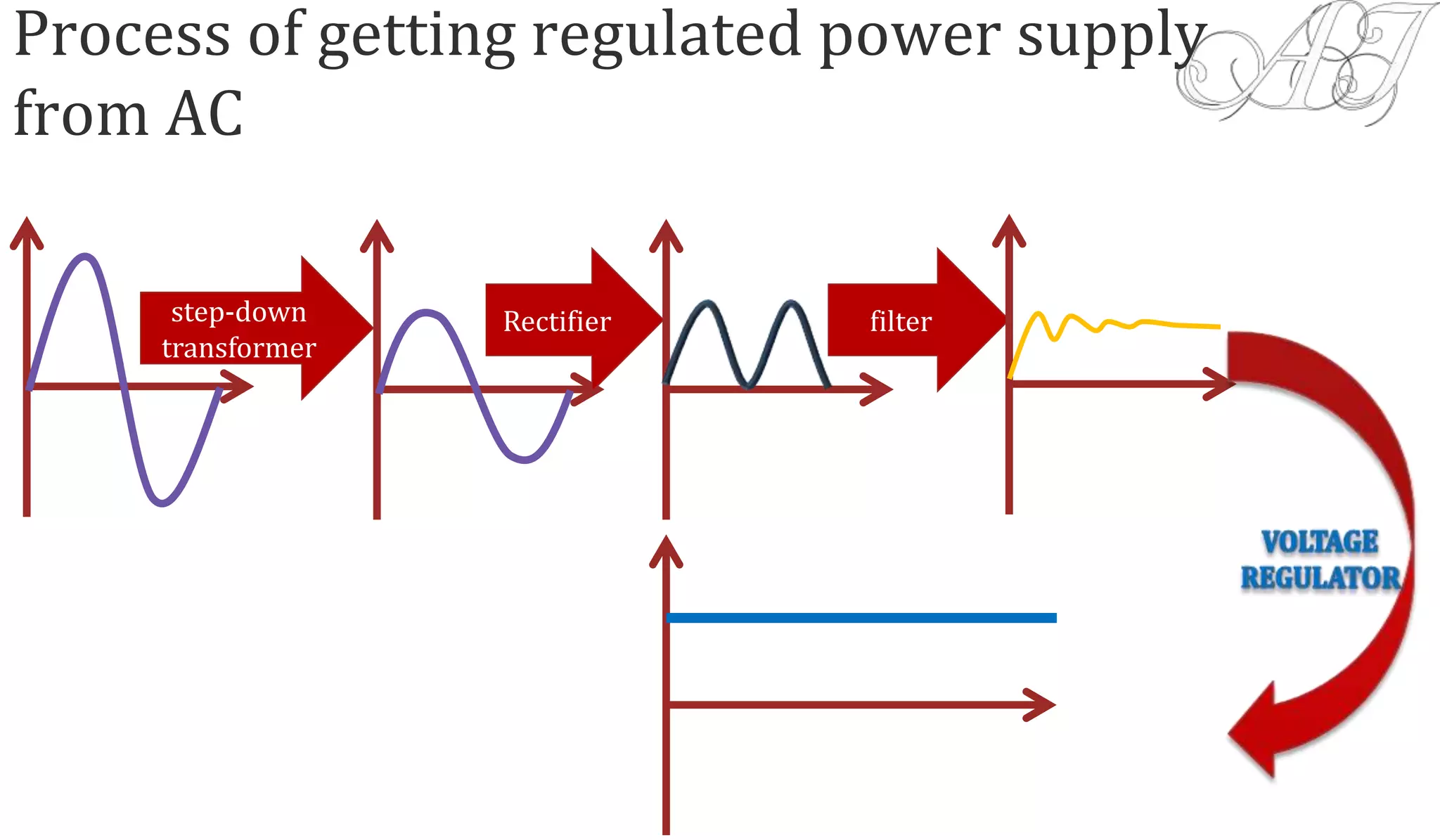
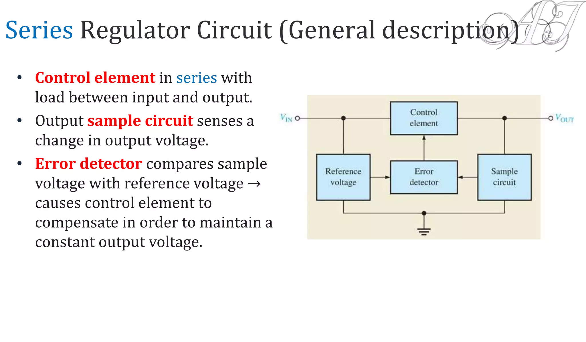
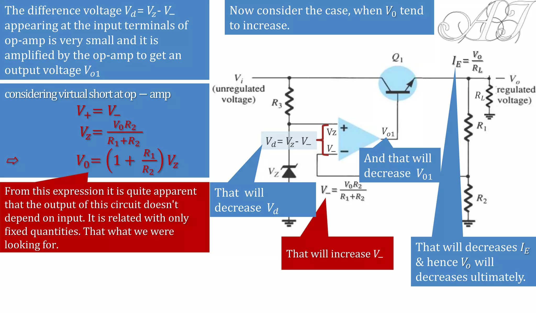
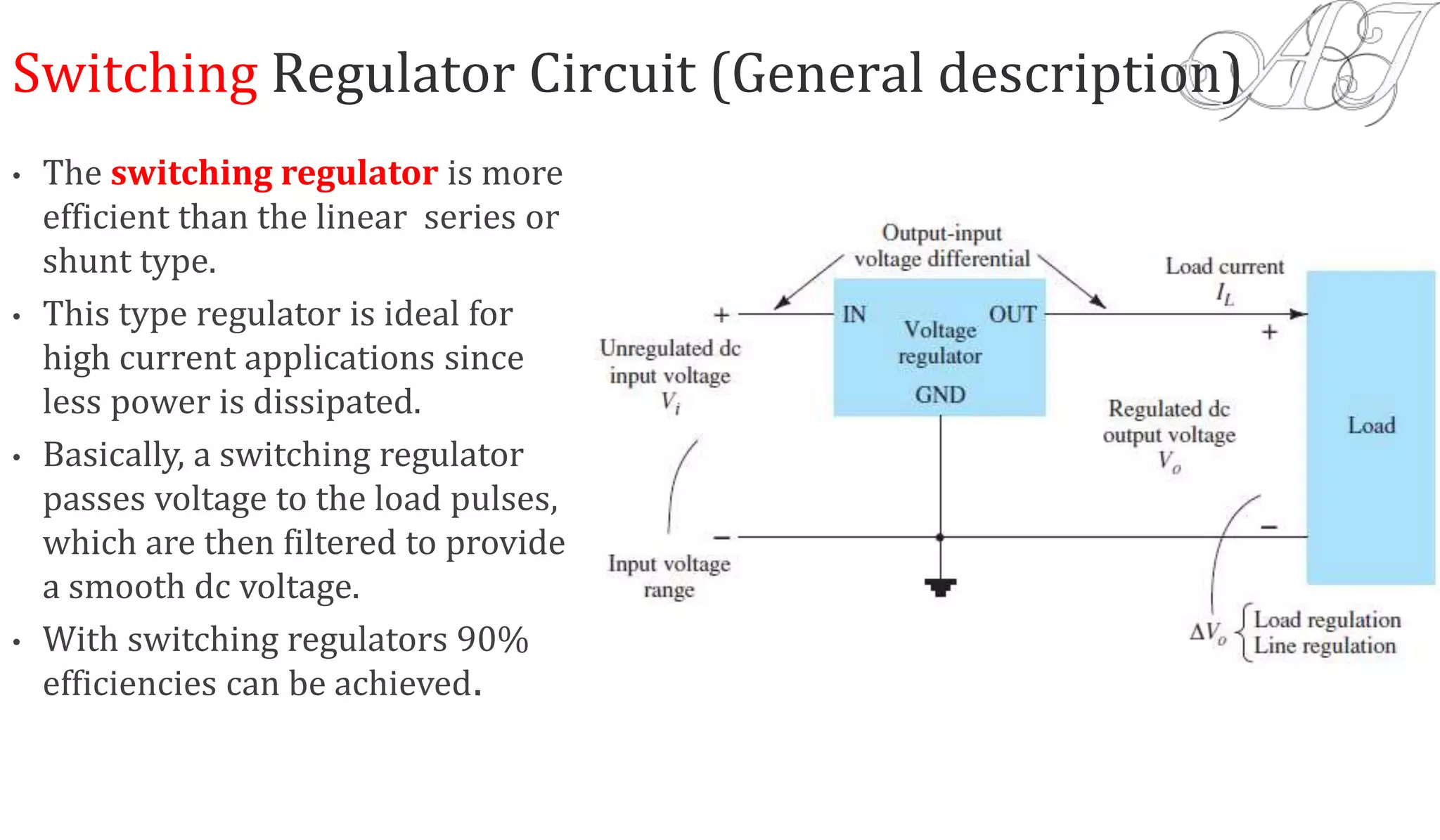
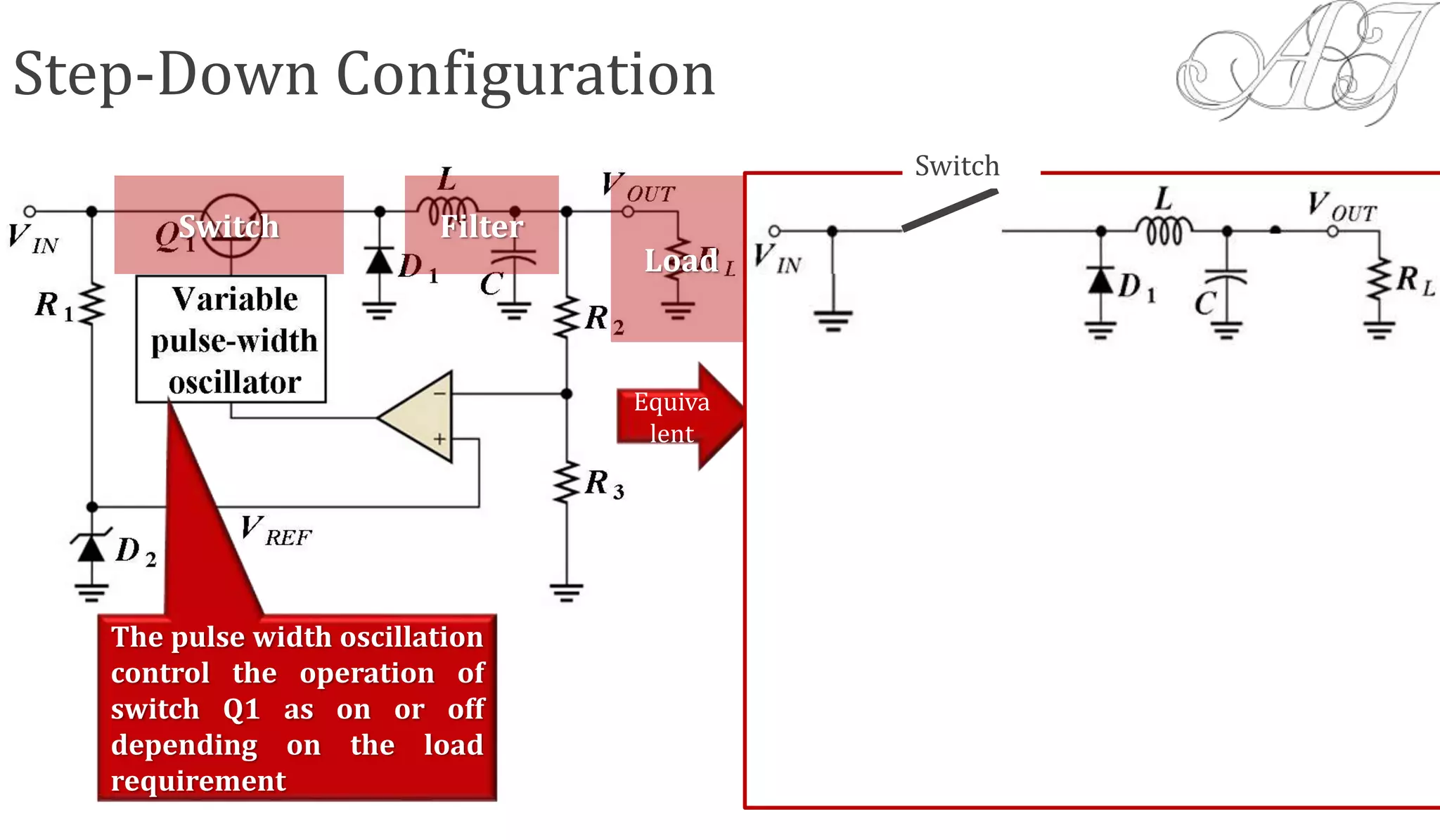
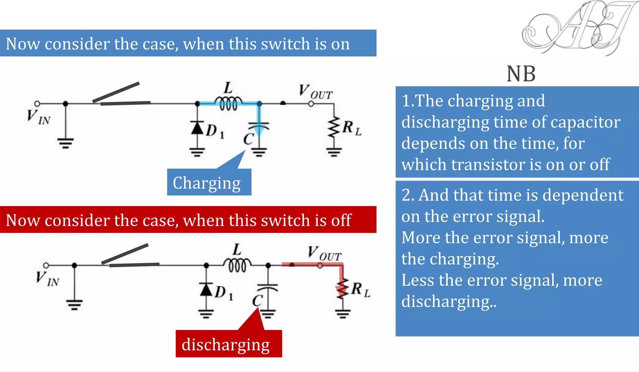
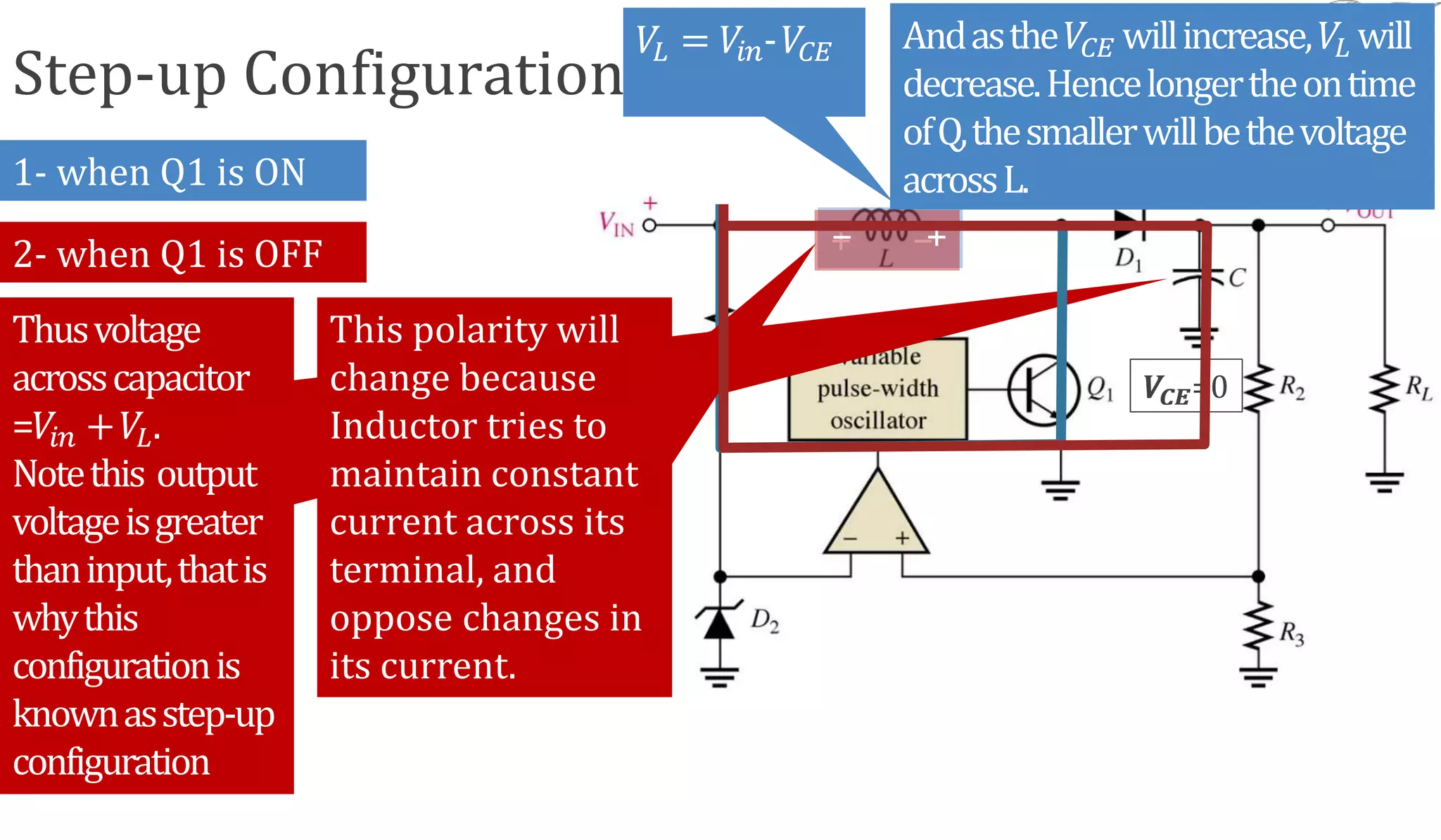
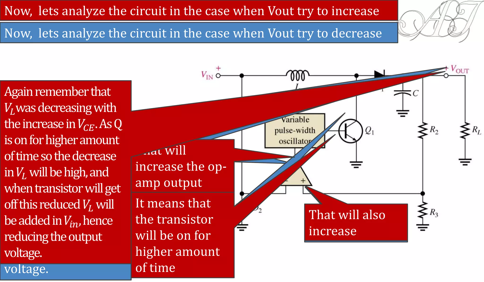
UNIT-5
Mohammad Asif Iqbal
Assistant Professor,
Deptt of ECE,
JETGI, Barabanki
Have you seen them ever?
In any circuit?
Introduction
• Batteries are often shown on a schematic diagram as the source of DC
voltage but usually the actual DC voltage source is a power supply.
• There are many types of power supply. Most are designed to convert high
voltage AC mains electricity to a suitable low voltage supply for
electronics circuits and other devices.
• A more reliable method of obtaining DC power is to transform, rectify,
filter and regulate an AC line voltage.
• This can be achieved with the help of Voltage Regulators
• It converts unregulated power supply into regulated one.
• The performance of a voltage regulated circuit is analyzed in terms of its
regulation
• For better performance of the circuit. % regulation must be as small as
possible.
step-down
transformer
Rectifier filter
Process of getting regulated power supply
from AC
Types of Regulator
Voltage
Regulator
Linear
Regulators
Series
Regulators
Shunt
Regulators
Switching
Regulators
Step-Down
Configuration
Step-up
Configuration
Voltage-
inverter
configuration
Series Regulator Circuit (General description)
• Control element in series with
load between input and output.
• Output sample circuit senses a
change in output voltage.
• Error detector compares sample
voltage with reference voltage →
causes control element to
compensate in order to maintain a
constant output voltage.
Op-Amp Series Regulator
Zener diode is a constant voltage
device or reference voltage
R3 is limiting resistance and it will
limit the zener current
Zener voltage Vz is appearing as
voltage at non inverting terminal of
op-amp
R1 and R2 are potential divider
network and 𝑉−=
𝑉0 𝑅2
𝑅1+𝑅2
This voltage 𝑉− is appearing at the
inverting input terminal of op-amp.
The emitter current 𝐼 𝐸 =
𝑉𝑜
𝑅1+𝑅2
+
𝑉𝑜
𝑅 𝐿
; if (𝑅1 + 𝑅2)⫺ 𝑅 𝐿 then 𝐼 𝐸 = 𝐼𝐿=
𝑉𝑜
𝑅 𝐿
𝑅 𝐿
Vz
𝑉−
𝑉𝑑= 𝑉𝑧- 𝑉−
𝐼 𝐸
𝑉𝑜1
Control Element
Error Detector Sample
Circuit
The difference voltage 𝑉𝑑= 𝑉𝑧- 𝑉−
appearing at the input terminals of
op-amp is very small and it is
amplified by the op-amp to get an
output voltage 𝑉𝑜1
consideringvirtualshortatop−amp
𝑉+= 𝑉−
𝑉𝑧=
𝑉0 𝑅2
𝑅1+𝑅2
⇨ 𝑉0= 1 +
𝑅1
𝑅2
𝑉𝑧
𝑅 𝐿
Vz
𝑉−
𝑉𝑑= 𝑉𝑧- 𝑉−
𝑉𝑜1
From this expression it is quite apparent
that the output of this circuit doesn't
depend on input. It is related with only
fixed quantities. That what we were
looking for.
𝐼 𝐸=
𝑉𝑜
𝑅 𝐿
Now consider the case, when 𝑉0 tend
to increase.
𝑉−=
𝑉0 𝑅2
𝑅1+𝑅2
That will increase 𝑉−
That will
decrease 𝑉𝑑
And that will
decrease 𝑉01
That will decreases 𝐼 𝐸
& hence 𝑉𝑜 will
decreases ultimately.
Shunt Regulator Circuit (General description)
• The control element is in parallel with load
• The unregulated input voltage provides
current to the load.
• Some of the current is pulled away by the
control element.
• If the load voltage tries to change due to a
change in the load resistance, the sampling
circuit provides a feedback signal to a
comparator.
• The resulting difference voltage then
provides a control signal to vary the
amount of the current shunted away from
the load to maintain the regulated output
voltage across the load.
Op-Amp Shunt Regulator
That will increase
𝑉+
That will
increase 𝑉𝑑
And that will
increase 𝑉01
Now consider the case, when 𝑉0 tend
to increase.
Vz
𝑉+
𝑉𝑑= 𝑉+ − 𝑉𝑧
𝑉𝑜1
𝑉+=
𝑉0 𝑅2
𝑅1+𝑅2
And that will
increase 𝐼SH
Now, since 𝐼SH+ 𝐼L is
constant, this increment in
𝐼SH will ultimately
decrease the 𝐼𝐿 and that
will decrease 𝑉𝑜
Switching Regulator Circuit (General description)
• The switching regulator is more
efficient than the linear series or
shunt type.
• This type regulator is ideal for
high current applications since
less power is dissipated.
• Basically, a switching regulator
passes voltage to the load pulses,
which are then filtered to provide
a smooth dc voltage.
• With switching regulators 90%
efficiencies can be achieved.
Step-Down Configuration
Switch Filter
The pulse width oscillation
control the operation of
switch Q1 as on or off
depending on the load
requirement
Equiva
lent
Load
Switch
Now consider the case, when this switch is on
Charging
Now consider the case, when this switch is off
discharging
NB
1.The charging and
discharging time of capacitor
depends on the time, for
which transistor is on or off
2. And that time is dependent
on the error signal.
More the error signal, more
the charging.
Less the error signal, more
discharging..
Now, lets analyze the circuit in the case when Vout try to decrease
That will decrease
𝑉−
It means that the
transistor will be
on for higher
amount of time
And that will
increase 𝑉01
It will increase
the charging time
and decrease the
discharging time
& hence the
output voltage
Now, lets analyze the circuit in the case when Vout try to increase
That will increase
𝑉−
And that will
decrease 𝑉01
It means that the
transistor will be
on for smaller
amount of time
It will decrease
the charging time
and increase the
discharging time
& hence the
output voltage
Another
important
discussion
𝑑𝑢𝑡𝑦 𝑐𝑦𝑐𝑙𝑒
𝛿 =
𝑡 𝑜𝑛
𝑡 𝑜𝑛 + 𝑡 𝑜𝑓𝑓
Step-up Configuration
1- when Q1 is ON
𝑉𝐿 = 𝑉𝑖𝑛-𝑉𝐶𝐸
𝑉𝐶𝐸
Andasthe 𝑉𝐶𝐸 willincrease, 𝑉𝐿 will
decrease.Hencelongertheontime
ofQ,thesmallerwillbethevoltage
acrossL.
2- when Q1 is OFF
𝑉𝐶𝐸=0
Thusvoltage
acrosscapacitor
=𝑉𝑖𝑛 +𝑉𝐿.
Notethis output
voltageisgreater
thaninput,thatis
whythis
configurationis
knownasstep-up
configuration
+ −
+−
This polarity will
change because
Inductor tries to
maintain constant
current across its
terminal, and
oppose changes in
its current.
Now, lets analyze the circuit in the case when Vout try to decrease
That will also
decrease
That will reduce
the op-amp
output
It means that
the transistor
will be on for
smaller amount
of time
Remember 𝑉𝐿was
decreasing with the
increase in 𝑉𝐶𝐸. As Q
is on for smaller time
so the decrease in 𝑉𝐿
will be low, and
when transistor will
get off this 𝑉𝐿 will be
added in 𝑉𝑖𝑛and
compensate the
decrease in output
voltage.
Now, lets analyze the circuit in the case when Vout try to increase
That will also
increase
That will
increase the op-
amp output
It means that
the transistor
will be on for
higher amount
of time
Againrememberthat
𝑉𝐿wasdecreasingwith
theincreasein 𝑉𝐶𝐸.AsQ
isonforhigheramount
oftimesothedecrease
in 𝑉𝐿 willbehigh,and
whentransistorwillget
offthisreduced 𝑉𝐿 will
beaddedin 𝑉𝑖𝑛,hence
reducingtheoutput
voltage.
THANK YOU!

voltage regulater

  • 1.
    UNIT-5 Mohammad Asif Iqbal AssistantProfessor, Deptt of ECE, JETGI, Barabanki
  • 2.
    Have you seenthem ever? In any circuit?
  • 3.
    Introduction • Batteries areoften shown on a schematic diagram as the source of DC voltage but usually the actual DC voltage source is a power supply. • There are many types of power supply. Most are designed to convert high voltage AC mains electricity to a suitable low voltage supply for electronics circuits and other devices. • A more reliable method of obtaining DC power is to transform, rectify, filter and regulate an AC line voltage. • This can be achieved with the help of Voltage Regulators • It converts unregulated power supply into regulated one. • The performance of a voltage regulated circuit is analyzed in terms of its regulation • For better performance of the circuit. % regulation must be as small as possible.
  • 4.
    step-down transformer Rectifier filter Process ofgetting regulated power supply from AC
  • 5.
  • 6.
    Series Regulator Circuit(General description) • Control element in series with load between input and output. • Output sample circuit senses a change in output voltage. • Error detector compares sample voltage with reference voltage → causes control element to compensate in order to maintain a constant output voltage.
  • 7.
    Op-Amp Series Regulator Zenerdiode is a constant voltage device or reference voltage R3 is limiting resistance and it will limit the zener current Zener voltage Vz is appearing as voltage at non inverting terminal of op-amp R1 and R2 are potential divider network and 𝑉−= 𝑉0 𝑅2 𝑅1+𝑅2 This voltage 𝑉− is appearing at the inverting input terminal of op-amp. The emitter current 𝐼 𝐸 = 𝑉𝑜 𝑅1+𝑅2 + 𝑉𝑜 𝑅 𝐿 ; if (𝑅1 + 𝑅2)⫺ 𝑅 𝐿 then 𝐼 𝐸 = 𝐼𝐿= 𝑉𝑜 𝑅 𝐿 𝑅 𝐿 Vz 𝑉− 𝑉𝑑= 𝑉𝑧- 𝑉− 𝐼 𝐸 𝑉𝑜1 Control Element Error Detector Sample Circuit
  • 8.
    The difference voltage𝑉𝑑= 𝑉𝑧- 𝑉− appearing at the input terminals of op-amp is very small and it is amplified by the op-amp to get an output voltage 𝑉𝑜1 consideringvirtualshortatop−amp 𝑉+= 𝑉− 𝑉𝑧= 𝑉0 𝑅2 𝑅1+𝑅2 ⇨ 𝑉0= 1 + 𝑅1 𝑅2 𝑉𝑧 𝑅 𝐿 Vz 𝑉− 𝑉𝑑= 𝑉𝑧- 𝑉− 𝑉𝑜1 From this expression it is quite apparent that the output of this circuit doesn't depend on input. It is related with only fixed quantities. That what we were looking for. 𝐼 𝐸= 𝑉𝑜 𝑅 𝐿 Now consider the case, when 𝑉0 tend to increase. 𝑉−= 𝑉0 𝑅2 𝑅1+𝑅2 That will increase 𝑉− That will decrease 𝑉𝑑 And that will decrease 𝑉01 That will decreases 𝐼 𝐸 & hence 𝑉𝑜 will decreases ultimately.
  • 9.
    Shunt Regulator Circuit(General description) • The control element is in parallel with load • The unregulated input voltage provides current to the load. • Some of the current is pulled away by the control element. • If the load voltage tries to change due to a change in the load resistance, the sampling circuit provides a feedback signal to a comparator. • The resulting difference voltage then provides a control signal to vary the amount of the current shunted away from the load to maintain the regulated output voltage across the load.
  • 10.
    Op-Amp Shunt Regulator Thatwill increase 𝑉+ That will increase 𝑉𝑑 And that will increase 𝑉01 Now consider the case, when 𝑉0 tend to increase. Vz 𝑉+ 𝑉𝑑= 𝑉+ − 𝑉𝑧 𝑉𝑜1 𝑉+= 𝑉0 𝑅2 𝑅1+𝑅2 And that will increase 𝐼SH Now, since 𝐼SH+ 𝐼L is constant, this increment in 𝐼SH will ultimately decrease the 𝐼𝐿 and that will decrease 𝑉𝑜
  • 11.
    Switching Regulator Circuit(General description) • The switching regulator is more efficient than the linear series or shunt type. • This type regulator is ideal for high current applications since less power is dissipated. • Basically, a switching regulator passes voltage to the load pulses, which are then filtered to provide a smooth dc voltage. • With switching regulators 90% efficiencies can be achieved.
  • 12.
    Step-Down Configuration Switch Filter Thepulse width oscillation control the operation of switch Q1 as on or off depending on the load requirement Equiva lent Load Switch
  • 13.
    Now consider thecase, when this switch is on Charging Now consider the case, when this switch is off discharging NB 1.The charging and discharging time of capacitor depends on the time, for which transistor is on or off 2. And that time is dependent on the error signal. More the error signal, more the charging. Less the error signal, more discharging..
  • 14.
    Now, lets analyzethe circuit in the case when Vout try to decrease That will decrease 𝑉− It means that the transistor will be on for higher amount of time And that will increase 𝑉01 It will increase the charging time and decrease the discharging time & hence the output voltage Now, lets analyze the circuit in the case when Vout try to increase That will increase 𝑉− And that will decrease 𝑉01 It means that the transistor will be on for smaller amount of time It will decrease the charging time and increase the discharging time & hence the output voltage Another important discussion 𝑑𝑢𝑡𝑦 𝑐𝑦𝑐𝑙𝑒 𝛿 = 𝑡 𝑜𝑛 𝑡 𝑜𝑛 + 𝑡 𝑜𝑓𝑓
  • 15.
    Step-up Configuration 1- whenQ1 is ON 𝑉𝐿 = 𝑉𝑖𝑛-𝑉𝐶𝐸 𝑉𝐶𝐸 Andasthe 𝑉𝐶𝐸 willincrease, 𝑉𝐿 will decrease.Hencelongertheontime ofQ,thesmallerwillbethevoltage acrossL. 2- when Q1 is OFF 𝑉𝐶𝐸=0 Thusvoltage acrosscapacitor =𝑉𝑖𝑛 +𝑉𝐿. Notethis output voltageisgreater thaninput,thatis whythis configurationis knownasstep-up configuration + − +− This polarity will change because Inductor tries to maintain constant current across its terminal, and oppose changes in its current.
  • 16.
    Now, lets analyzethe circuit in the case when Vout try to decrease That will also decrease That will reduce the op-amp output It means that the transistor will be on for smaller amount of time Remember 𝑉𝐿was decreasing with the increase in 𝑉𝐶𝐸. As Q is on for smaller time so the decrease in 𝑉𝐿 will be low, and when transistor will get off this 𝑉𝐿 will be added in 𝑉𝑖𝑛and compensate the decrease in output voltage. Now, lets analyze the circuit in the case when Vout try to increase That will also increase That will increase the op- amp output It means that the transistor will be on for higher amount of time Againrememberthat 𝑉𝐿wasdecreasingwith theincreasein 𝑉𝐶𝐸.AsQ isonforhigheramount oftimesothedecrease in 𝑉𝐿 willbehigh,and whentransistorwillget offthisreduced 𝑉𝐿 will beaddedin 𝑉𝑖𝑛,hence reducingtheoutput voltage.
  • 17.