Downloaded 293 times

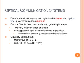
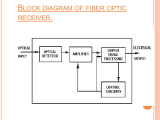
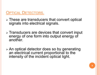
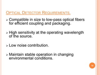
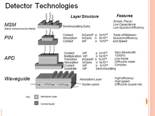
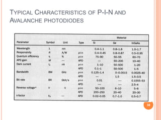
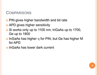

This document presents information on optical detectors. It begins with an overview of optical communication systems and fiber optic architecture. It then discusses the key components of optical receivers including light sources, detectors, and fiber-optic cables. Common types of optical detectors are photo diodes (PIN and APD). PIN diodes have good linearity and speed but lower sensitivity, while APDs provide internal gain but more noise. Characteristics like responsivity, bandwidth, capacitance, and noise are examined. Factors influencing detector performance and tradeoffs between bandwidth and efficiency are also summarized.