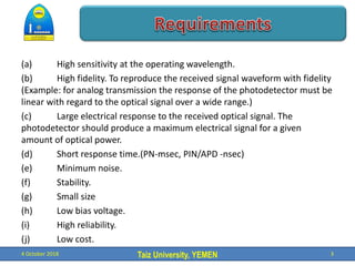
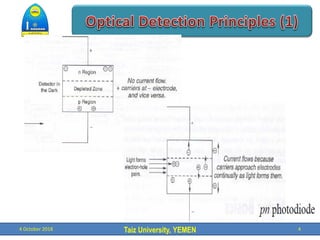
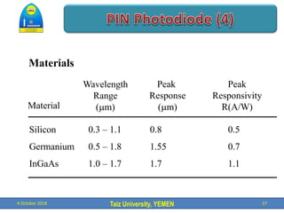
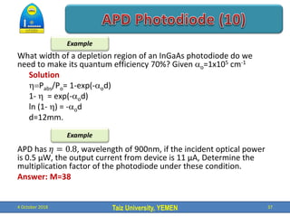
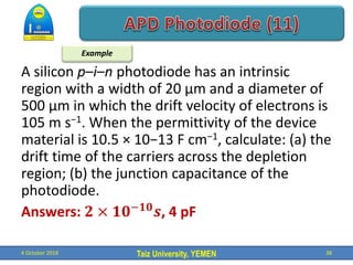
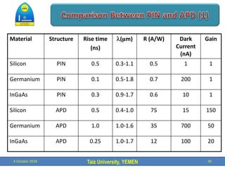
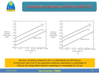
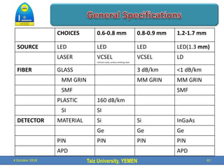
2. Taiz University, YEMEN
• A detector’s function is to convert the received
optical signal into an electrical signal, which is
then amplified before further processing.
• Therefore when considering signal attenuation
along the link, the system performance is
determined at the detector. Improvement of
detector characteristics and performance thus
allows the installation of fewer repeater stations
and lowers both the capital investment and
maintenance costs.
4 October 2018 2
3. Taiz University, YEMEN
(a) High sensitivity at the operating wavelength.
(b) High fidelity. To reproduce the received signal waveform with fidelity
(Example: for analog transmission the response of the photodetector must be
linear with regard to the optical signal over a wide range.)
(c) Large electrical response to the received optical signal. The
photodetector should produce a maximum electrical signal for a given
amount of optical power.
(d) Short response time.(PN-msec, PIN/APD -nsec)
(e) Minimum noise.
(f) Stability.
(g) Small size
(h) Low bias voltage.
(i) High reliability.
(j) Low cost.
4 October 2018 3
5. Taiz University, YEMEN
• This device is reverse biased and the electric field
developed across the p-n junction sweeps mobile
carriers (holes and electrons) to their respective
majority sides (p and n type material).
• A depletion region or layer is therefore created on
either side of the junction.
• This barrier has the effect of stopping the majority
carriers crossing the junction in the opposite direction
to the field.
• However, the field accelerates minority carriers from
both sides to the opposite side of the junction, forming
the reverse leakage current of the diode.
4 October 2018 5
6. Taiz University, YEMEN
• A photon incident in or near the depletion region of this device which has
an energy greater than or equal to the bandgap energy E of the
fabricating material (i.e. hf > Eg) will excite an electron from the valence
band (VB) into the conduction band (CB).
• This process leaves an empty hole in the valence band and is known as the
photogeneration of an electron-hole (carrier) pair as shown in the
following Figure (a).
• Carrier pairs so generated near the junction are separated and swept
(drift) under the influence of the electric field to produce a displacement
current in the external circuit in excess of any reverse leakage current
(Fig.(b)).
• Photogeneration and the separation of a carrier pair in the depletion
region of this reverse biased p-n junction is illustrated in Fig.(c).
4 October 2018 6
7. Taiz University, YEMEN
4 October 2018 7
Operation of the p–n photodiode: (a) photogeneration of an electron–hole pair in an intrinsic
semiconductor; (b) the structure of the reverse-biased p–n junction illustrating carrier drift in the
depletion region; (c) the energy band diagram of the reverse-biased p–n junction showing
photogeneration and the subsequent separation of an electron–hole pair
8. Taiz University, YEMEN
• The depletion region must be sufficiently thick to allow
a large fraction of the incident light to be absorbed in
order to achieve maximum carrier pair generation. (PN
1 to 3 mm PIN 20 to 50 mm).
• However, since long carrier drift times in the depletion
region restrict the speed of operation of the
photodiode it is necessary to limit its width.
• Absorption outside depletion region-diffusion current-
reduces speed. Absorption inside depletion region-drift
current-fast due to the large electrical field.
4 October 2018 8
9. Taiz University, YEMEN
• The absorption of photons in a photodiode to
produce carrier pairs and thus a photocurrent, is
dependent on the absorption coefficient α0 of the
light in the semiconductor used to fabricate the
device. α0 strongly dependent on wavelength. Light
falling on a photodiode- partially absorbed and
partially transmitted. Pabs = power absorbed and Po =
power incident.
4 October 2018 9
)
exp(
1
( d
P
P o
o
abs
10. Taiz University, YEMEN
• At a specific wavelength the photocurrent Ip
produced by incident light of optical power P0 is
given by:
where e is the charge on an electron, r is the
Fresnel reflection coefficient at the semiconductor-
air interface and d is the width of the absorption
region. When α0 goes to zero, Pabs goes to zero.
When α0 goes to infinity Po = Pabs.
4 October 2018 10
d
hf
r
e
P
I p 0
0
exp
1
1
11. Taiz University, YEMEN
4 October 2018 11
Optical absorption curves for some common semiconductor photodiode materials
12. Taiz University, YEMEN
• For a given semiconductor material, the
photodiode can detect only wavelengths
l<lc = hc/Eg.
• If Eg is specified in eV then λc can be written as
lc = 1.24/Eg (mm)
• For wavelengths longer than λc, the photons will
travel through the material without interaction.
Si – 1100nm and InGaAs – 1700 nm.
4 October 2018 12
13. Taiz University, YEMEN
• The quantum efficiency η is defined as the fraction of incident
photons which are absorbed by the photodetector and
generate electrons which are collected at the detector
terminals:
𝜂 =
𝑛𝑢𝑚𝑏𝑒𝑟 𝑜𝑓 𝑒𝑙𝑒𝑐𝑡𝑟𝑜𝑛𝑠 𝑐𝑜𝑙𝑙𝑒𝑐𝑡𝑒𝑑
𝑛𝑢𝑚𝑏𝑒𝑟 𝑜𝑓 𝑖𝑛𝑐𝑖𝑑𝑒𝑛𝑡 𝑝ℎ𝑜𝑡𝑜𝑛𝑠
where rp is the incident photon rate (photons per second) and re
is the corresponding electron rate (electrons per second).
4 October 2018 13
hf
P
e
I
r
r
o
p
p
e
/
/
14. Taiz University, YEMEN
• One of the major factors which determines the
quantum efficiency is the absorption coefficient
of the semiconductor material used within the
photodetector.
• The quantum efficiency is generally less than
unity as not all of the incident photons are
absorbed to create electron-hole pairs.
• Finally, in common with the absorption
coefficient, the quantum efficiency is a function
of the photon wavelength and must therefore
only be quoted for a specific wavelength.
4 October 2018 14
15. Taiz University, YEMEN
Responsivity, R is defined as:
where Ip is the output photocurrent in amperes and P0 is
the incident optical power in watts. Typical value ranges
from 0.5 A/W to 1.0 A/W
• The responsivity is a useful parameter as it gives the
transfer characteristic of the detector (i.e.
photocurrent per unit incident optical power).
4 October 2018 15
1
0
AW
P
I
R
p
16. Taiz University, YEMEN
• The relationship for responsivity may be developed to
include quantum efficiency as follows:
• This equation may be developed a further stage to include
the wavelength of the incident light where λ is in nm.
• The ideal responsivity against wavelength characteristic for
a silicon photodiode with unit quantum efficiency is
illustrated in next Figure.
4 October 2018 16
1
AW
hf
e
R
)
(
1248
nm
hc
e
R l
l
17. Taiz University, YEMEN
• Responsivity vs. wavelength
4 October 2018 17
Responsivity against wavelength characteristics: (a) an ideal silicon photodiode with a typical
device also shown; (b) silicon, germanium and InGaAs photodiodes with quantum efficiencies.
18. Taiz University, YEMEN
When 3 × 10¹¹ photons each with a wavelength of 0.85 μm are
incident on a photodiode, on average 1.2 × 10¹¹
electrons are
collected at the terminals of the device. Determine the quantum
efficiency and the responsivity of the photodiode at 0.85 μm.
Answers: 0.4, 0.274 A W−1
A photodiode has a quantum efficiency of 65% when photons of
energy 1.5 × 10⁻¹⁹
J are incident upon it.
(a) At what wavelength is the photodiode operating?
(b) Calculate the incident optical power required to obtain a
photocurrent of 2.5 μA when the photodiode is operating as described
above.
Answers: 1.32 μm, 3.60 μW
4 October 2018 18
Example
Example
19. Taiz University, YEMEN
• Semiconductor diodes can be classified into two categories
that is with internal gain and without internal gain.
• Semiconductor photodiodes without internal gain generate a
single electron hole pair per absorbed photon.
• Three types of photodiodes will be discussed later:
4 October 2018 19
PN Photodiode (1st Class).
PIN Photodiode (1st Class).
Avalanche Photodiode (APD) (2nd Class).
20. Taiz University, YEMEN
• The depletion region is formed by immobile
positively charged donor atoms in the n type
semiconductor material and immobile negatively
charged acceptor atoms in the p type material,
when the mobile carriers are swept to their
majority sides under the influence of the electric
field.
• The width of the depletion region is therefore
dependent upon the doping concentrations for a
given applied reverse bias (i.e. the lower the
doping, the wider the depletion region).
4 October 2018 20
21. Taiz University, YEMEN
4 October 2018 21
The p–n photodiode showing depletion and diffusion regions
22. Taiz University, YEMEN
• In the depletion region, the carrier pairs separate and drift
under the influence of the electric field, whereas outside this
region the hole diffuses towards the depletion region in order
to be collected.
• The diffusion process is very slow compared to the drift
process and thus limits the response of the photodiode
• It is therefore important that the photons are absorbed in the
depletion region.
• Thus it is made as long as possible by decreasing the doping in
the n type material.
4 October 2018 22
23. Taiz University, YEMEN
• The depletion region width in a p-n photodiode is normally 1-3 µm and is
optimized for the efficient detection of light at a given wavelength.
• Typical output characteristics for the reverse-biased p-n photodiode is illustrated in
the following Figure.
• The different operating conditions may be noted moving from no light input to a
high light level.
4 October 2018 23
24. Taiz University, YEMEN
• In order to allow operation at longer wavelengths
where the light penetrates more deeply into the
semiconductor material a wider depletion region
is necessary.
• To achieve this the n type material is doped so
lightly that it can be considered intrinsic, and to
make a low resistance contact a highly doped n
type (n+ ) layer is added.
• This creates a p-i-n (or PIN) structure as may be
seen in the following Figure where almost all the
absorption takes place in the depletion region.
4 October 2018 24
25. Taiz University, YEMEN
4 October 2018 25
The p–i–n photodiode showing the combined absorption and depletion region
26. Taiz University, YEMEN
• The high electric field present in the depletion region
causes photo-generated carriers to separate and be
collected across the reverse –biased junction. This
give rise to a current flow in an external circuit,
known as photocurrent.
4 October 2018 26
28. Taiz University, YEMEN
• The APD has a more sophisticated structure than the p-
i-n photodiode in order to create an extremely high
electric field region.
• Therefore, as well as the depletion region where most
of the photons are absorbed and the primary carrier
pairs generated there is a high field region in which
holes and electrons can acquire sufficient energy to
excite new electron-hole pairs.
• This process is known as impact ionization and is the
phenomenon that leads to avalanche breakdown in
ordinary reverse biased diodes.
4 October 2018 28
29. Taiz University, YEMEN
• It requires very high reverse bias voltages (100-400 V) in order that
the new carriers created by impact ionization can themselves
produce additional carriers by the same mechanism as shown in
next Fig.(b).
• Carrier multiplication factors as great as 105 may be obtained using
defect free materials to ensure uniformity of carrier multiplication
over the entire photosensitive area.
• High reverse voltage. This accelerates electrons and holes
thereupon acquires high energy. They strike neutral atoms and
generates more free charge carriers. These secondary charges then
ionize other carriers.
• Primary generated electrons strike bonded electrons at the VB and
excite them to the CB. Known as Impact Ionization.
• The main advantage compared to pin photodiode is the
multiplication or gain factor, M.
4 October 2018 29
30. Taiz University, YEMEN
4 October 2018 30
(a) Avalanche photodiode showing high electric field (gain) region.
(b) Carrier pair multiplication in the gain region of an avalanche photodiode
31. Taiz University, YEMEN
The response time limited by three factors.
(1) The transit time of the carriers across the absorption
region (i.e. the depletion width)
(2) The time taken by the carriers to perform the
avalanche multiplication process.
(3) The RC time constant incurred by the junction
capacitance of the diode and its load.
4 October 2018 31
32. Taiz University, YEMEN
• Often an asymmetric pulse shape is obtained
from the APD which results from a relatively fast
rise time as the electrons are collected and a fall
time dictated by the transit time of the holes
travelling at a slower speed.
• Hence, although the use of suitable materials and
structures may give rise times between 150 and
200 ps, fall times of 1 ns or more are quite
common which limit the overall response of the
device.
4 October 2018 32
33. Taiz University, YEMEN
Drawbacks of the APD
(a) Fabrication difficulties due to their more
complex structure and hence increased cost.
(b) The random nature of the gain mechanism
which gives an additional noise contribution
(c) The high bias voltages required (100-400 V).
(d) The variation of the gain with temperature as
shown in next Fig. for a silicon APD.
4 October 2018 33
34. Taiz University, YEMEN
4 October 2018 34
Current gain against reverse bias for a silicon RAPD operating at a wavelength of 0.825 μm.
35. Taiz University, YEMEN
• Multiplication Factor
• The multiplication factor M is a measure of the internal gain provided by the
APD.
• It is defined as:
where I is the total output current at the operating voltage and Ip is the initial or
primary photocurrent.
• The gain M, increases
with the reverse bias voltage, Vd.
where n = constant and VBR is the breakdown voltage of the detector which is
usually around 20 to 500V.
• The responsivity of APD can be calculated by considering the current gain as:
4 October 2018 35
p
I
I
M
n
BR
d
V
V
M
1
1
M
R
M
hf
e
R 0
APD
36. Taiz University, YEMEN
• Bandwidth: maximum frequency or bit rate that a photo diode can detect.
Determined by the response time.
The response time limited by three factors.
(1) The transit time of the carriers across the absorption region, =d/vsat
(2) The RC time constant incurred by the junction capacitance (Cj)of the diode
and its load. Cj =/d. is the permittivity of the semiconductor and A is
the active area of the photodiode.
(3) The time taken by the carriers to perform the avalanche multiplication
process (for APD).
• vsat=saturation velocity.
• Large area collects more light but reduces BW.
4 October 2018 36
37. Taiz University, YEMEN
What width of a depletion region of an InGaAs photodiode do we
need to make its quantum efficiency 70%? Given o=1x105 cm-1
Solution
Pabs/Po= 1-exp(-od)
1- = exp(-od)
ln (1- ) = -od
d=12mm.
APD has 𝜂 = 0.8, wavelength of 900nm, if the incident optical power
is 0.5 µW, the output current from device is 11 µA, Determine the
multiplication factor of the photodiode under these condition.
Answer: M=38
4 October 2018 37
Example
Example
38. Taiz University, YEMEN
A silicon p–i–n photodiode has an intrinsic
region with a width of 20 μm and a diameter of
500 μm in which the drift velocity of electrons is
105 m s−1. When the permittivity of the device
material is 10.5 × 10⁻¹³ F cm−1, calculate: (a) the
drift time of the carriers across the depletion
region; (b) the junction capacitance of the
photodiode.
Answers: 𝟐 × 𝟏𝟎−𝟏𝟎
𝒔, 4 pF
4 October 2018 38
Example
39. Taiz University, YEMEN
4 October 2018 39
Material Structure Rise time
(ns)
l(μm) R (A/W) Dark
Current
(nA)
Gain
Silicon PIN 0.5 0.3-1.1 0.5 1 1
Germanium PIN 0.1 0.5-1.8 0.7 200 1
InGaAs PIN 0.3 0.9-1.7 0.6 10 1
Silicon APD 0.5 0.4-1.0 75 15 150
Germanium APD 1.0 1.0-1.6 35 700 50
InGaAs APD 0.25 1.0-1.7 12 100 20
40. Taiz University, YEMEN
4 October 2018 40
Receiver sensitivity comparison of p–i–n photodiode and APD devices
at a bit-error-rate of 10−9: (a) using silicon detectors operating at a wavelength of
0.82 μm; (b) using InGaAs detectors operating at a wavelength of 1.55 μm
41. Taiz University, YEMEN
4 October 2018 41
CHOICES 0.6-0.8 mm 0.8-0.9 mm 1.2-1.7 mm
SOURCE LED LED LED LED(1.3 mm)
LASER VCSEL
Vertical-cavity surface-emitting laser
VCSEL LD
FIBER GLASS 3 dB/km <1 dB/km
MM GRIN MM GRIN MM GRIN
SMF SMF
PLASTIC 160 dB/km
SI SI
DETECTOR MATERIAL Si Si InGaAs
Ge Ge Ge
PIN PIN PIN PIN
APD APD