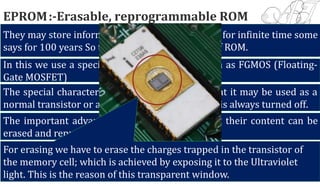
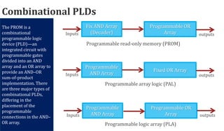
Download to read offline

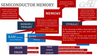
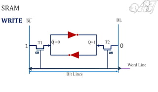
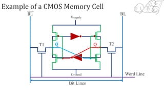
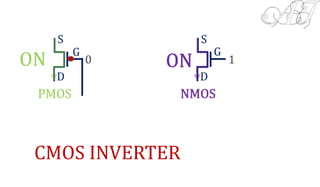
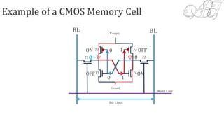
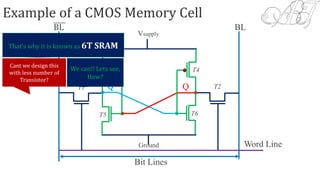
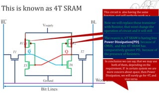
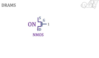
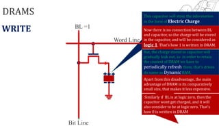
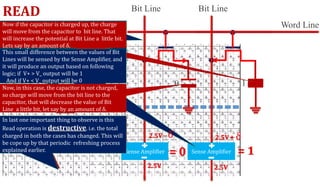
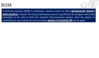
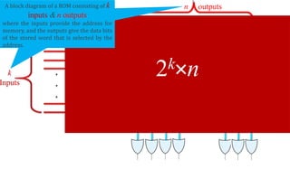
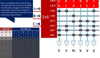
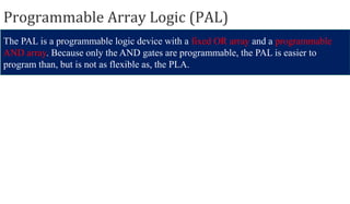
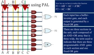


The document discusses various memory elements used in computers, focusing on the differences between primary memory (RAM) and secondary memory (ROM, PROM, EEPROM). It explains their structures, functionality, and the distinctions in volatile and non-volatile memory types, including the advantages and disadvantages of SRAM and DRAM. Additionally, it covers programmable logic devices like PLA and PAL, detailing their architectures and the process of programming these devices.