Downloaded 111 times

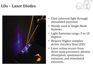
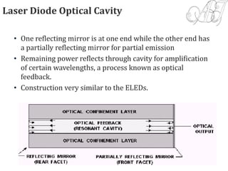
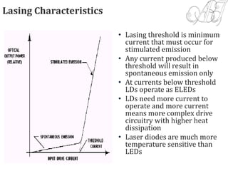


Optical sources convert electrical signals to optical signals for data transmission through fiber optic cables. They include LEDs, ELEDs, SLEDs, and laser diodes (LDs). LEDs produce incoherent light while laser diodes produce coherent light. Incoherent light sources are used for multimode fiber systems while laser diodes are used for single mode systems. Laser diodes must operate above the lasing threshold to produce coherent light, otherwise they function as ELEDs. Tunable lasers can produce coherent light of a controlled variable wavelength, allowing them to replace multiple light sources in multi-wavelength transmission systems.