Downloaded 191 times


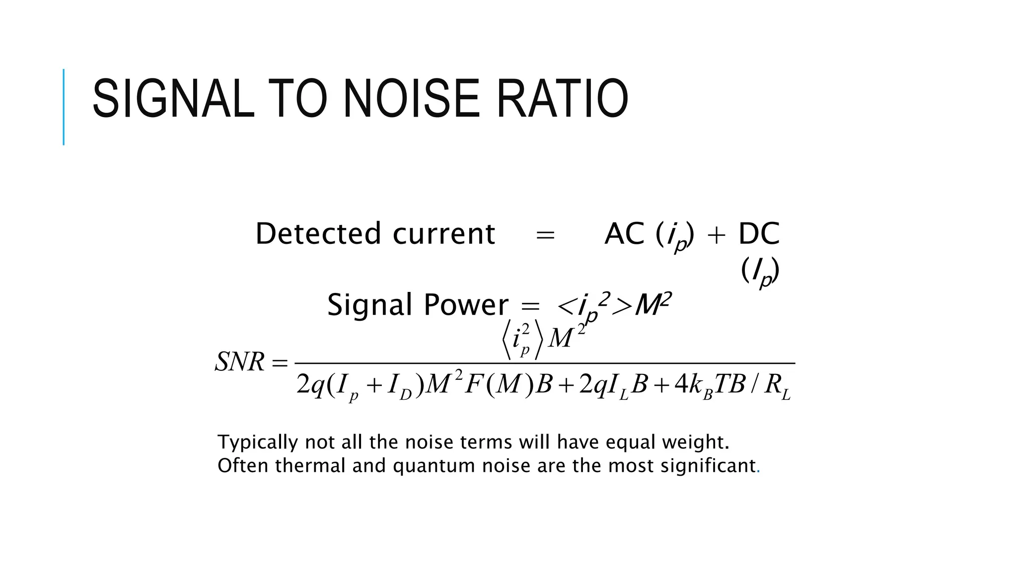

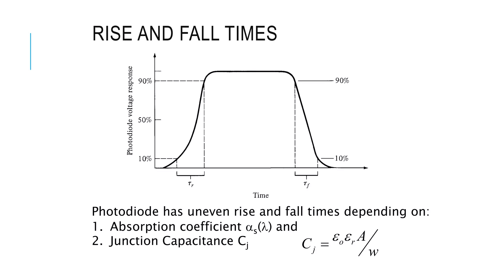
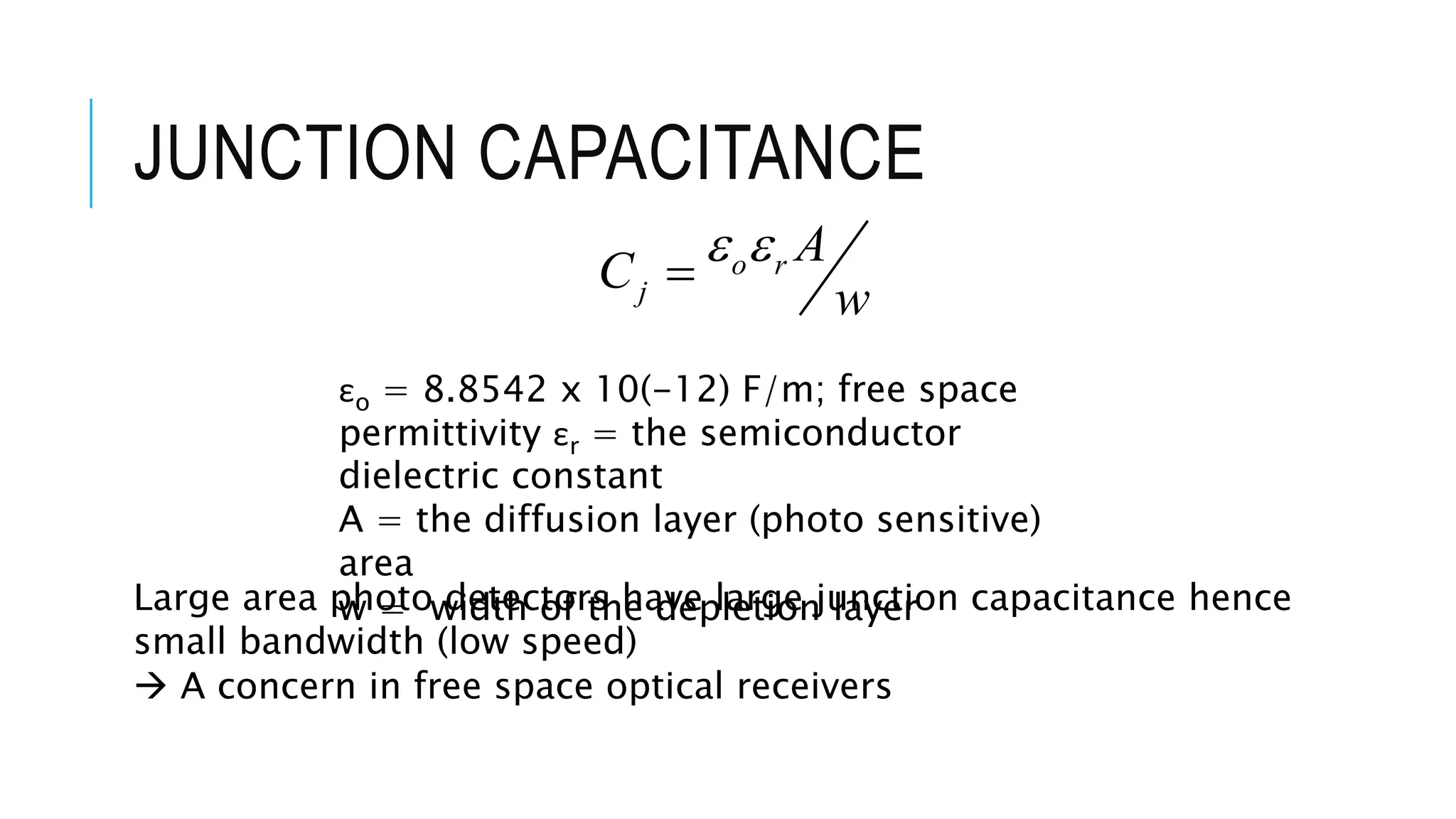
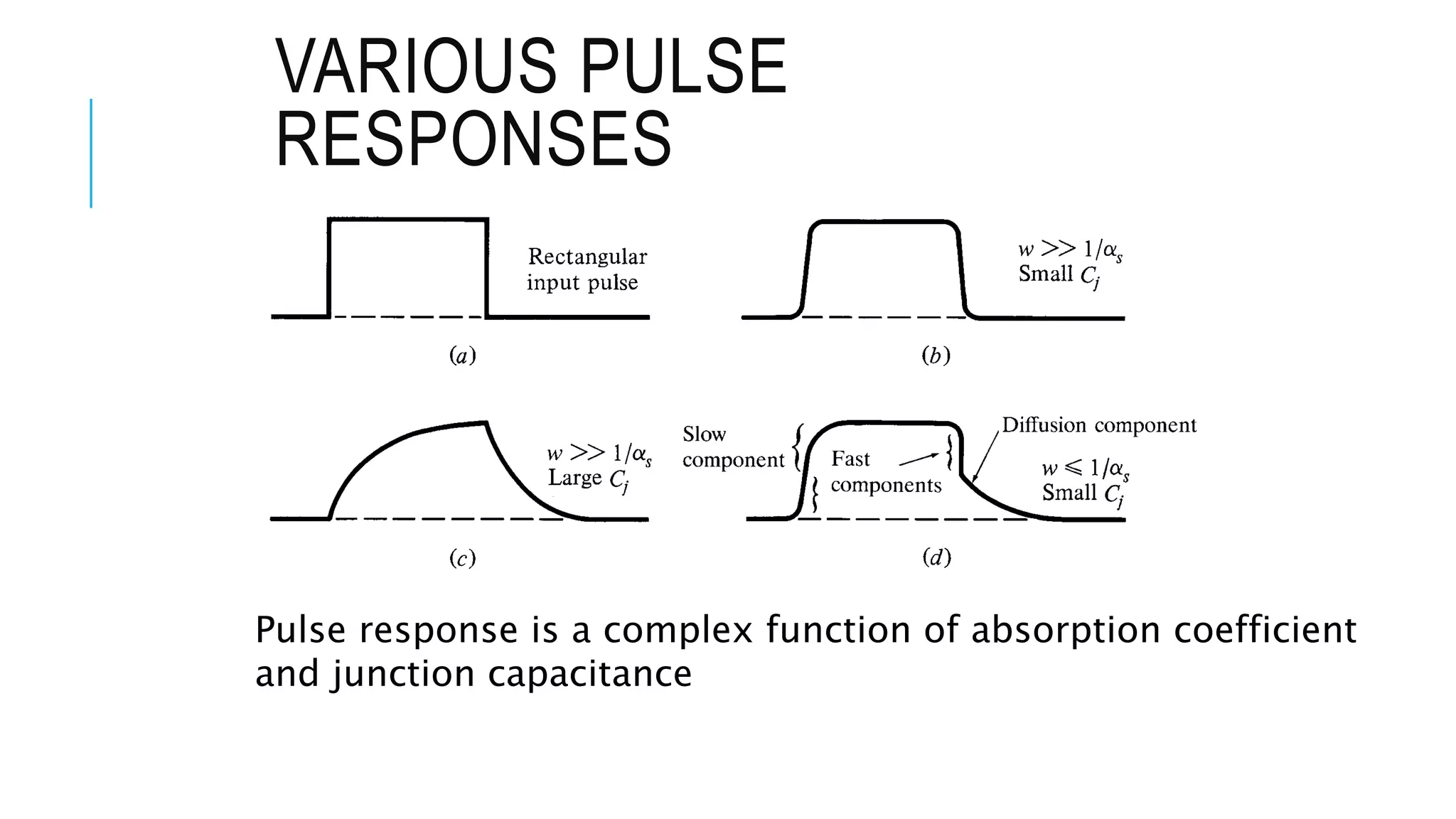


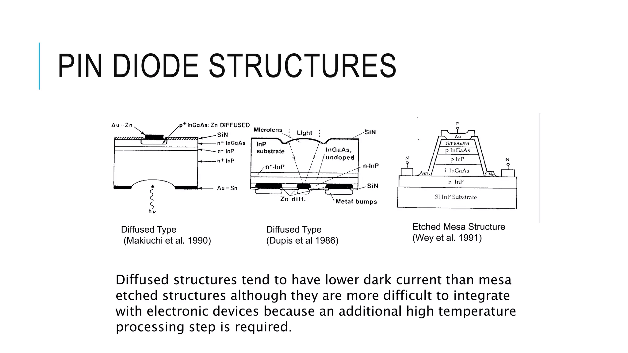


This document summarizes key aspects of PIN photodiodes. It describes the physical principles of how PIN photodiodes operate by separating photo-generated carriers across a reverse-biased junction to produce a photocurrent. It also discusses photodiode characteristics like quantum efficiency and responsivity. Additionally, it covers noise sources in photodetector circuits including quantum, dark current, leakage current, and thermal noise. The document also examines photodiode response time and how the junction capacitance and absorption coefficient impact the rise and fall times. Finally, it compares different PIN photodiode structures like front vs rear illuminated and diffused vs mesa etched designs.


