Downloaded 148 times

![Error Sources in DTS
!
)(
)(
0
n
e
NnP
E
h
dttP
h
N
N
n
r
is the average number of electron-hole pairs in photodetector,
is the detector quantum efficiency and E is energy received in a time
interval and is photon energy, where is the probability
that n electrons are emitted in an interval .
N
h )(nPr
[7-
1]
[7-2]](https://image.slidesharecdn.com/unit-5-170605053900/85/OPTICAL-COMMUNICATION-Unit-5-3-320.jpg)
![Receiver Configuration
The binary digital pulse train incident on the photodetector can be written in the
following form:
t.allforpositiveiswhichshapepulsereceivedtheis)(and
digitmessageththeofparameteramplitudeanisperiod,bitiswhere
)()(
th
nbT
nTthbtP
p
nb
n
bpn
[7-3]](https://image.slidesharecdn.com/unit-5-170605053900/85/OPTICAL-COMMUNICATION-Unit-5-5-320.jpg)
![• In writing down eq. [7-3], we assume the digital pulses with amplitude V
represents bit 1 and 0 represents bit 0. Thus can take two values
corresponding to each binary data. By normalizing the input pulse to
the photodiode to have unit area
represents the energy in the nth pulse.
the mean output current from the photodiode at time t resulting from pulse
train given in eq. [7-3] is (neglecting the DC components arising from dark
current noise):
nb
)(thp
1)( dtthp
nb
n
bpno nTthbMtMP
h
q
ti )()()(
[7-4]](https://image.slidesharecdn.com/unit-5-170605053900/85/OPTICAL-COMMUNICATION-Unit-5-6-320.jpg)
![Bit Error Rate (BER)
• Probability of Error= probability that the output voltage is
less than the threshold when a 1 is sent + probability that the
output voltage is more than the threshold when a 0 has been
sent.
b
e
t
e
TB
Bt
N
N
N
t
t
/1
duringedtransmittpulsesof#total
intervalmecertain tiaovererrorof#
ErrorofyProbabilitBER
[7-5]](https://image.slidesharecdn.com/unit-5-170605053900/85/OPTICAL-COMMUNICATION-Unit-5-7-320.jpg)
![Probability distributions for received logical 0 and 1 signal pulses.
the different widths of the two distributions are caused by various signal
distortion effects.
thv
edtransmitt0if,exceedstageoutput volequalizerthat theprobablity)0|()(
edtransmitt1if,thanlessistageoutput volequalizerthat theprobablity)1|()(
0
1
vdyypvP
vdyypvP
v
v
[7-6]](https://image.slidesharecdn.com/unit-5-170605053900/85/OPTICAL-COMMUNICATION-Unit-5-8-320.jpg)
![• Where are the probabilities that the transmitter sends 0 and 1
respectively.
• For an unbiased transmitter
th
th
v
v
ththe
dyypqdyypq
vPqvPqP
)1|()1|(
)()(
01
0011
[7-7]
01 and qq
5.010 qq
10 1 qq ](https://image.slidesharecdn.com/unit-5-170605053900/85/OPTICAL-COMMUNICATION-Unit-5-9-320.jpg)
![Gaussian Distribution
dv
bv
dyypvP
dv
bv
dyypvP
thth
thth
vv
th
v
on
v
th
2
off
2
off
off
0
2
on
2
on
1
2
)(
exp
2
1
)0|()(
2
)(
exp
2
1
)1|()(
mea
n
mea
n
[7-8]](https://image.slidesharecdn.com/unit-5-170605053900/85/OPTICAL-COMMUNICATION-Unit-5-10-320.jpg)
![• If we assume that the probabilities of 0 and 1 pulses are equally likely, then
using eq [7-7] and [7-8] , BER becomes:
Q
Q
Q
dxxQP
Q
e
/2)exp(-
2
1
)
2
(erf1
2
1
)exp(
1
)(BER
2
2/
2
[7-9]
dyyx
vbbv
Q
x
thth
0
2
on
on
off
off
)exp(
2
)(erf
[7-9]
[7-10]](https://image.slidesharecdn.com/unit-5-170605053900/85/OPTICAL-COMMUNICATION-Unit-5-11-320.jpg)
![Approximation of error function
Variation of BER vs Q,
according to eq [7-9].](https://image.slidesharecdn.com/unit-5-170605053900/85/OPTICAL-COMMUNICATION-Unit-5-12-320.jpg)
![Special Case
In special case when:
Vbb onoffonoff ,0&
From eq [7-29], we have: 2/Vvth
Eq [7-8] becomes:
)
22
(erf1
2
1
)(
V
Pe
[7-11]
Study example 7-1 pp. 286 of the textbook.
ratio.noise-rms-to-signalpeakis
V](https://image.slidesharecdn.com/unit-5-170605053900/85/OPTICAL-COMMUNICATION-Unit-5-13-320.jpg)
![Quantum Limit
• Minimum received power required for a specific BER assuming that the
photodetector has a 100% quantum efficiency and zero dark current. For
such ideal photo-receiver,
• Where is the average number of electron-hole pairs, when the incident
optical pulse energy is E and given by eq [7-1] with 100% quantum
efficiency .
• Eq [7-12] can be derived from eq [7-2] where n=0.
• Note that, in practice the sensitivity of receivers is around 20 dB higher than
quantum limit because of various nonlinear distortions and noise effects in
the transmission link.
)exp()0(1 NPPe [7-12]
N
)1( ](https://image.slidesharecdn.com/unit-5-170605053900/85/OPTICAL-COMMUNICATION-Unit-5-14-320.jpg)
![Existing Work
• Eye diagram analysis
• Analytical eye-diagram model [Hashimoto, CICC’07]
• Only consider attenuation and reflection
• Assume perfect match at transmitter end
• Jitter and noise analysis
• Data-dependent jitter model [Buckwalter, MicrowaveSymp’04][Ou’DTS’04]
• Only consider two taps of channel response
• Enumerate all possible input combinations: [00, 01, 10, 11]
• Clock jitter model [Hanumolu’04][Tao’99]
• Clock-data recovery (CDR), DLL, PLL
• Amplitude noise model [Hanumolu’05]
• No general framework to model the jitter and noise and find
out what is the worst possible scenario](https://image.slidesharecdn.com/unit-5-170605053900/85/OPTICAL-COMMUNICATION-Unit-5-17-320.jpg)
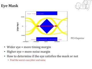
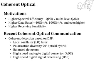
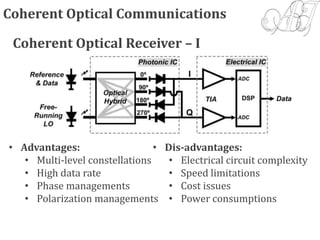
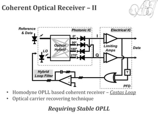
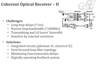
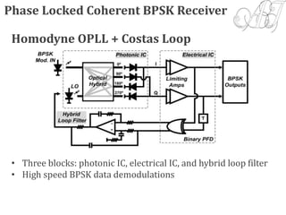
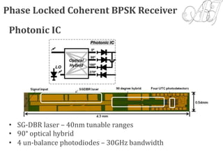


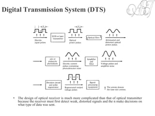
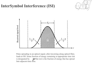
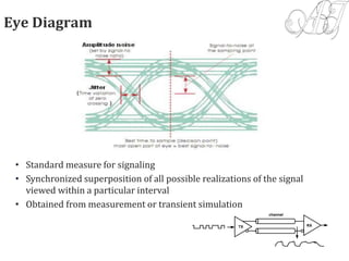
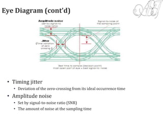
The document discusses digital transmission systems and coherent optical communications. It covers the following key points: 1) It describes the components and operation of optical receivers, including the challenges of detecting weak signals and making decisions on transmitted data. Error sources like intersymbol interference are also discussed. 2) Bit error rate and probability of error are defined, and formulas for calculating BER under Gaussian noise are provided. 3) Eye diagrams are introduced as a way to visualize signal quality over time. Factors like timing jitter and noise amplitude are described. 4) Coherent optical receivers are overviewed, including their advantages for high data rates and constellations. Challenges in carrier recovery using optical phase-locked