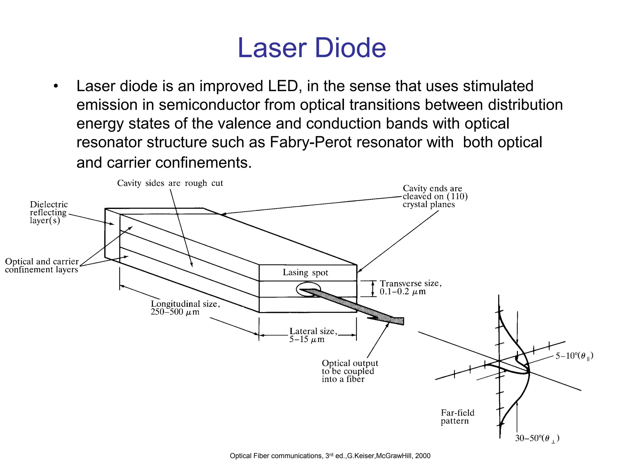
The document reviews key concepts in photonic sources, focusing on semiconductor physics, light-emitting diodes (LEDs), and laser diodes. It outlines structures, mechanisms, and performance characteristics of these light sources, including efficiency, modulation, and operational principles such as population inversion for laser action. Additionally, it explains the impact of material properties on light emission and the significance of rate equations in understanding device performance.


![Intrinsic & Extrinsic Materials
• Intrinsic material: A perfect material with no impurities.
• Extrinsic material: donor or acceptor type semiconductors.
• Majority carriers: electrons in n-type or holes in p-type.
• Minority carriers: holes in n-type or electrons in p-type.
• The operation of semiconductor devices is essentially based on
the injection and extraction of minority carriers.
)
2
exp(
T
k
E
n
p
n
B
g
i
ly.
respective
ions
concentrat
intrinsic
&
hole
electron,
the
are
&
& i
n
p
n
e.
Temperatur
is
energy,
gap
the
is T
Eg
2
i
n
pn
[4-1]
[4-2]](https://image.slidesharecdn.com/37-240326170031-a864a199/75/37-ocn_-ppt-Optimizing-slideshow-photodiiode-6-2048.jpg)


![Optical Fiber communications, 3rd ed.,G.Keiser,McGrawHill, 2000
Cross-section drawing of a typical
GaAlAs double heterostructure light
emitter. In this structure, x>y to provide
for both carrier confinement and optical
guiding.
b) Energy-band diagram showing the
active region, the electron & hole
barriers which confine the charge carriers
to the active layer.
c) Variations in the refractive index; the
lower refractive index of the material in
regions 1 and 5 creates an optical barrier
around the waveguide because of the higher
band-gap energy of this material.
)
eV
(
240
.
1
m)
(
g
E
[4-3]](https://image.slidesharecdn.com/37-240326170031-a864a199/75/37-ocn_-ppt-Optimizing-slideshow-photodiiode-13-2048.jpg)


![Rate equations, Quantum Efficiency & Power of
LEDs
• When there is no external carrier injection, the excess density
decays exponentially due to electron-hole recombination.
• n is the excess carrier density,
• Bulk recombination rate R:
• Bulk recombination rate (R)=Radiative recombination rate +
nonradiative recombination rate
/
0
)
( t
e
n
t
n
[4-4]
lifetime.
carrier
:
density
electron
excess
injected
initial
:
0
n
n
dt
dn
R
[4-5]](https://image.slidesharecdn.com/37-240326170031-a864a199/75/37-ocn_-ppt-Optimizing-slideshow-photodiiode-19-2048.jpg)
![)
1
rate(
ion
recombinat
ve
nonradiati
)
1
(
rate
ion
recombinat
radiative
)
1
(
rate
ion
recombinat
bulk
r nr
nr
r /τ
R
/τ
R
/τ
R
With an external supplied current density of J the rate equation for the electron-hole
recombination is:
region
ion
recombinat
of
thickness
:
electron;
the
of
charge
:
)
(
d
q
n
qd
J
dt
t
dn
[4-6]
In equilibrium condition: dn/dt=0
qd
J
n
[4-7]](https://image.slidesharecdn.com/37-240326170031-a864a199/75/37-ocn_-ppt-Optimizing-slideshow-photodiiode-20-2048.jpg)
![r
nr
r
nr
nr
r
r
R
R
R
int
Internal Quantum Efficiency & Optical Power
[4-8]
region
active
in the
efficiency
quantum
internal
:
int
Optical power generated internally in the active region in the LED is:
q
hcI
h
q
I
P int
int
int
[4-9]
region
active
current to
Injected
:
power,
optical
Internal
:
int
I
P](https://image.slidesharecdn.com/37-240326170031-a864a199/75/37-ocn_-ppt-Optimizing-slideshow-photodiiode-21-2048.jpg)
![External Quantum Eficiency
• In order to calculate the external quantum efficiency, we need to
consider the reflection effects at the surface of the LED. If we
consider the LED structure as a simple 2D slab waveguide, only
light falling within a cone defined by critical angle will be emitted
from an LED.
photons
generated
internally
LED
of
#
LED
from
emitted
photons
of
#
ext
[4-10]](https://image.slidesharecdn.com/37-240326170031-a864a199/75/37-ocn_-ppt-Optimizing-slideshow-photodiiode-22-2048.jpg)
![
d
T
c
)
sin
2
(
)
(
4
1
0
ext
[4-11]
2
2
1
2
1
)
(
4
)
0
(
t
Coefficien
on
Transmissi
Fresnel
:
)
(
n
n
n
n
T
T
[4-12]
2
1
1
ext
2
)
1
(
1
1
If
n
n
n [4-13]
2
1
1
int
int
ext
)
1
(
powr,
optical
emitted
LED
n
n
P
P
P [4-14]](https://image.slidesharecdn.com/37-240326170031-a864a199/75/37-ocn_-ppt-Optimizing-slideshow-photodiiode-23-2048.jpg)
![Modulation of LED
• The frequency response of an LED depends on:
1- Doping level in the active region
2- Injected carrier lifetime in the recombination region, .
3- Parasitic capacitance of the LED
• If the drive current of an LED is modulated at a frequency of
the output optical power of the device will vary as:
• Electrical current is directly proportional to the optical power,
thus we can define electrical bandwidth and optical bandwidth,
separately.
2
0
)
(
1
)
(
i
P
P
[4-15]
i
current
electrical
:
power,
electrical
:
)
0
(
log
20
)
0
(
10log
BW
Electrical
I
p
I
)
I(
p
)
p(
[4-16]](https://image.slidesharecdn.com/37-240326170031-a864a199/75/37-ocn_-ppt-Optimizing-slideshow-photodiiode-24-2048.jpg)
![
)
0
(
)
(
log
10
)
0
(
)
(
log
10
BW
Optical
I
I
P
P
[4-17]
Optical Fiber communications, 3rd ed.,G.Keiser,McGrawHill, 2000](https://image.slidesharecdn.com/37-240326170031-a864a199/75/37-ocn_-ppt-Optimizing-slideshow-photodiiode-25-2048.jpg)


![Fabry-Perot Resonator
A
B
L
M1 M2 m = 1
m = 2
m = 8
Relative intensity
m
m m + 1
m - 1
(a) (b) (c)
R ~ 0.4
R ~ 0.8
1 f
Schematic illustration of the Fabry-Perot optical cavity and its properties. (a) Reflected
waves interfere. (b) Only standing EM waves, modes, of certain wavelengths are allowed
in the cavity. (c) Intensity vs. frequency for various modes.R is mirror reflectance and
lower R means higher loss from the cavity.
© 1999 S.O. Kasap, Optoelectronics (Prentice Hall)
)
(
sin
4
)
1
(
)
1
(
2
2
2
kL
R
R
R
I
I inc
trans
[4-18]
R: reflectance of the optical intensity, k: optical wavenumber
1,2,3,..
:
modes
Resonant
m
m
kL ](https://image.slidesharecdn.com/37-240326170031-a864a199/75/37-ocn_-ppt-Optimizing-slideshow-photodiiode-29-2048.jpg)

![Laser Operation & Lasing Condition
• To determine the lasing condition and resonant frequencies, we
should focus on the optical wave propagation along the
longitudinal direction, z-axis. The optical field intensity, I, can be
written as:
• Lasing is the condition at which light amplification becomes
possible by virtue of population inversion. Then, stimulated
emission rate into a given EM mode is proportional to the
intensity of the optical radiation in that mode. In this case, the
loss and gain of the optical field in the optical path determine the
lasing condition. The radiation intensity of a photon at energy
varies exponentially with a distance z amplified by factor g, and
attenuated by factor according to the following relationship:
)
(
)
(
)
,
( z
t
j
e
z
I
t
z
I
[4-19]
h
](https://image.slidesharecdn.com/37-240326170031-a864a199/75/37-ocn_-ppt-Optimizing-slideshow-photodiiode-33-2048.jpg)
![
z
h
h
g
I
z
I )
(
)
(
exp
)
0
(
)
(
[4-20]
1
R 2
R
Z=0 Z=L
)
2
(
)
(
)
(
exp
)
0
(
)
2
( 2
1 L
h
h
g
R
R
I
L
I
[4-21]
2
2
1
2
1
t,
coefficien
absorption
effective
:
t
coefficien
gain
:
g
factor,
t
confinemen
Optical
:
n
n
n
n
R
α
1
n
2
n
Lasing Conditions:
1
)
2
exp(
)
0
(
)
2
(
L
j
I
L
I
[4-22]](https://image.slidesharecdn.com/37-240326170031-a864a199/75/37-ocn_-ppt-Optimizing-slideshow-photodiiode-34-2048.jpg)
![Threshold gain & current density
2
1
1
ln
2
1
R
R
L
gth
th
g
g
:
iff
lase"
"
to
starts
Laser
[4-23]
For laser structure with strong carrier confinement, the threshold current
Density for stimulated emission can be well approximated by:
th
th J
g
[4-24]
on
constructi
device
specific
on
depends
constant
:
](https://image.slidesharecdn.com/37-240326170031-a864a199/75/37-ocn_-ppt-Optimizing-slideshow-photodiiode-35-2048.jpg)
![Semiconductor laser rate equations
• Rate equations relate the optical output power, or # of photons per unit
volume, , to the diode drive current or # of injected electrons per
unit volume, n. For active (carrier confinement) region of depth d, the
rate equations are:
emission
stimulated
ion
recombinat
s
spontaneou
injection
rate
electron
loss
photon
emission
s
spontaneou
emission
stimulated
rate
Photon
Cn
n
qd
J
dt
dn
R
Cn
dt
d
sp
ph
sp
[4-25]
density
current
Injection
time
life
photon
mode
lasing
the
into
emission
s
spontaneou
of
rate
process
absorption
&
emission
optical
the
of
intensity
the
expressing
t
Coefficien
:
:
:
:
J
R
C
ph
sp
](https://image.slidesharecdn.com/37-240326170031-a864a199/75/37-ocn_-ppt-Optimizing-slideshow-photodiiode-37-2048.jpg)
![Threshold current Density & excess electron density
• At the threshold of lasing:
• The threshold current needed to maintain a steady state threshold
concentration of the excess electron, is found from electron rate
equation under steady state condition dn/dt=0 when the laser is just
about to lase:
0
,
0
/
,
0
sp
R
dt
d
th
ph
ph n
C
n
Cn
1
0
/
25]
-
[4
eq.
from [4-26]
sp
th
th
sp
th
th n
qd
J
n
qd
J
0 [4-27]](https://image.slidesharecdn.com/37-240326170031-a864a199/75/37-ocn_-ppt-Optimizing-slideshow-photodiiode-38-2048.jpg)
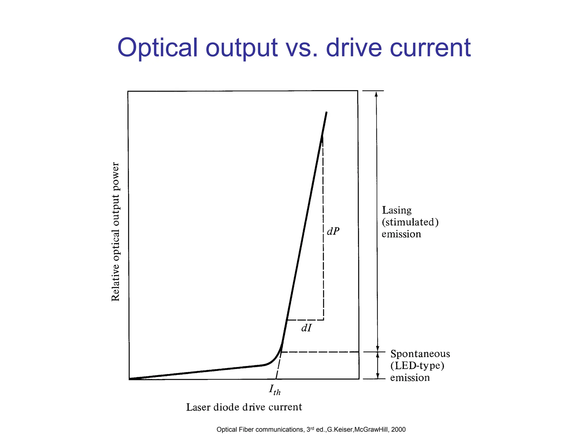
![Laser operation beyond the threshold
• The solution of the rate equations [4-25] gives the steady state
photon density, resulting from stimulated emission and
spontaneous emission as follows:
th
J
J
sp
ph
th
ph
s R
J
J
qd
)
( [4-28]](https://image.slidesharecdn.com/37-240326170031-a864a199/75/37-ocn_-ppt-Optimizing-slideshow-photodiiode-39-2048.jpg)
![External quantum efficiency
• Number of photons emitted per radiative electron-hole pair
recombination above threshold, gives us the external quantum
efficiency.
• Note that:
)
mA
(
)
mW
(
]
m
[
8065
.
0
)
(
dI
dP
dI
dP
E
q
g
g
g
th
th
i
ext
[4-29]
%
40
%
15
%;
70
%
60
ext
i
](https://image.slidesharecdn.com/37-240326170031-a864a199/75/37-ocn_-ppt-Optimizing-slideshow-photodiiode-40-2048.jpg)
![Laser Resonant Frequencies
• Lasing condition, namely eq. [4-22]:
• Assuming the resonant frequency of the mth
mode is:
,...
3
,
2
,
1
,
2
L
2
1
)
2
exp(
m
m
L
j
n
2
1,2,3,...
2
m
Ln
mc
m
Ln
Ln
c
m
m
2
2
2
1
[4-30]
[4-31]](https://image.slidesharecdn.com/37-240326170031-a864a199/75/37-ocn_-ppt-Optimizing-slideshow-photodiiode-41-2048.jpg)
![Spectrum from a laser Diode
width
spectral
:
2
)
(
exp
)
0
(
)
( 2
0
g
g [4-32]](https://image.slidesharecdn.com/37-240326170031-a864a199/75/37-ocn_-ppt-Optimizing-slideshow-photodiiode-42-2048.jpg)

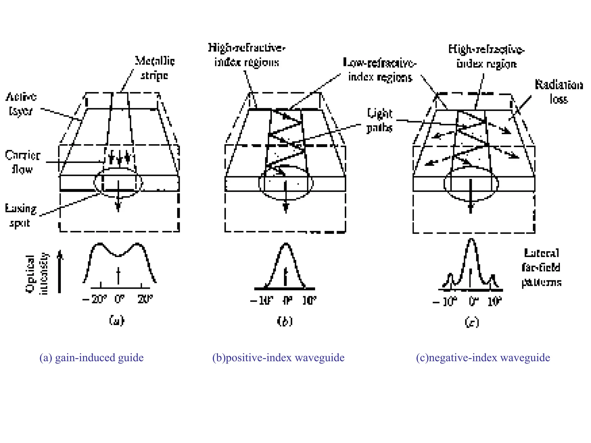
![Single Mode Laser
• Single mode laser is mostly based on the index-
guided structure that supports only the fundamental
transverse mode and the fundamental longitudinal
mode. In order to make single mode laser we have
four options:
1- Reducing the length of the cavity to the point
where the frequency separation given in eq[4-31] of
the adjacent modes is larger than the laser transition
line width. This is hard to handle for fabrication and
results in low output power.
2- Vertical-Cavity Surface Emitting laser (VCSEL)
3- Structures with built-in frequency selective grating
4- tunable laser diodes
.](https://image.slidesharecdn.com/37-240326170031-a864a199/75/37-ocn_-ppt-Optimizing-slideshow-photodiiode-46-2048.jpg)

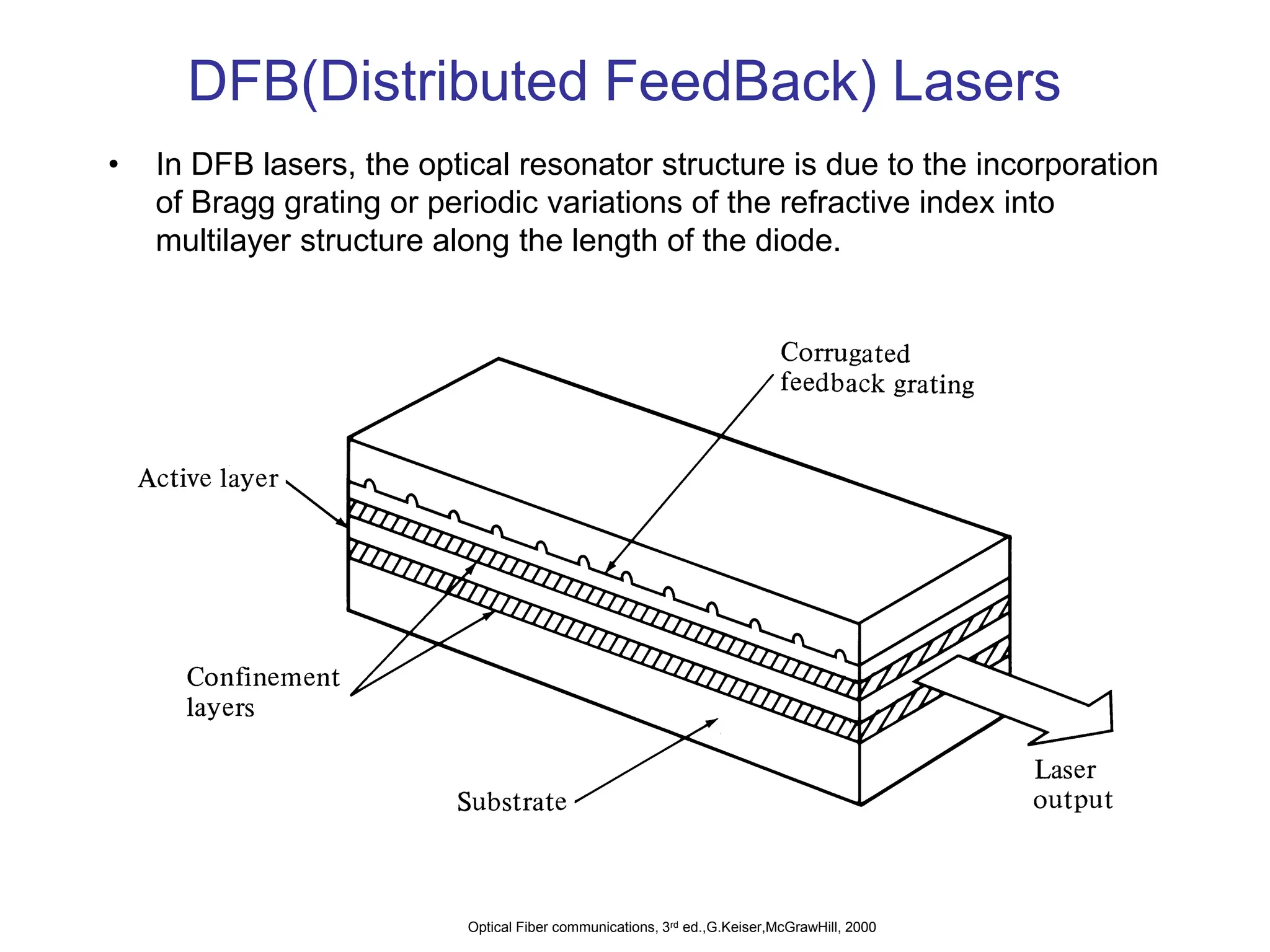
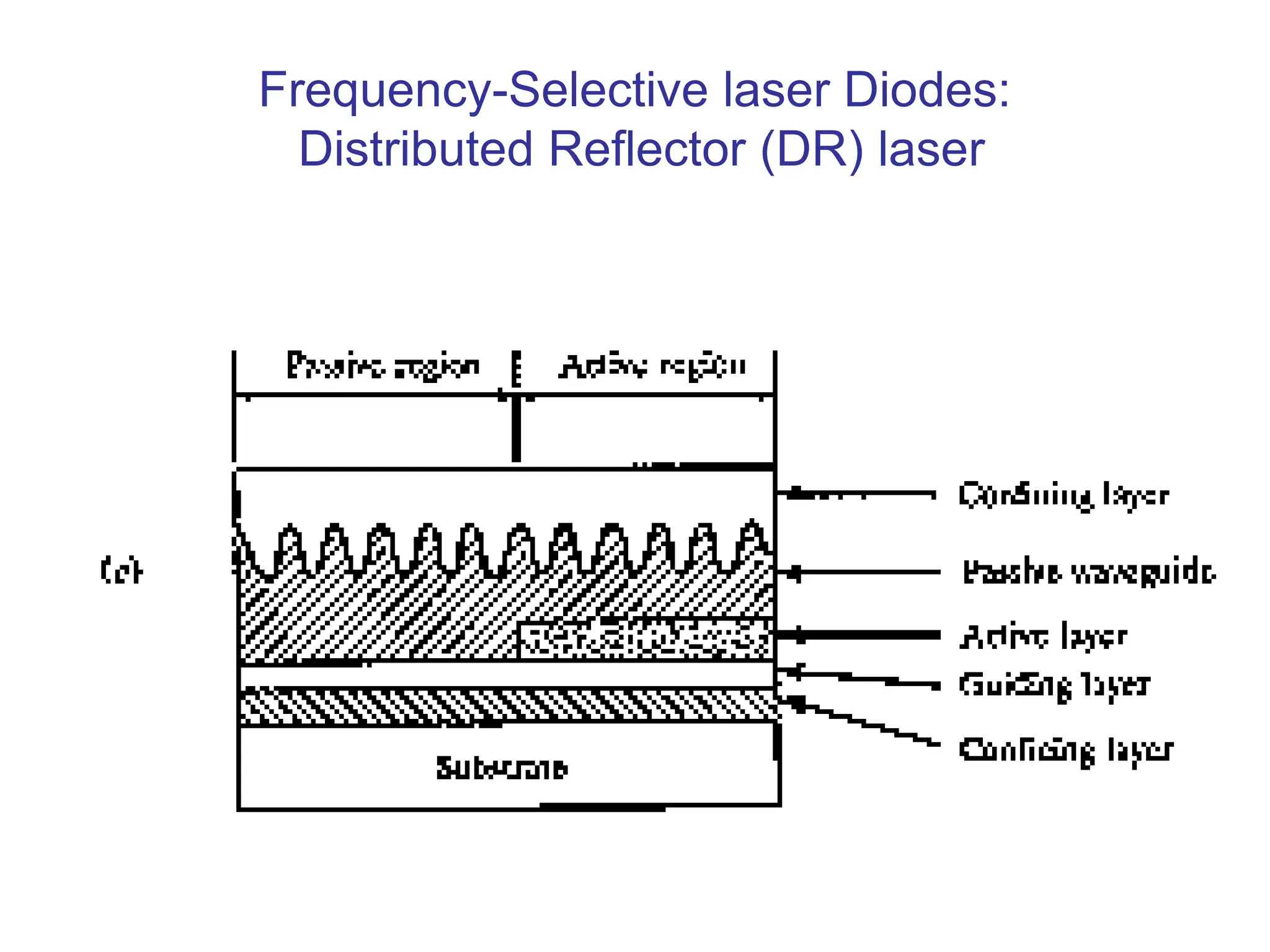
![Frequency-Selective laser Diodes:
Distributed Feedback (DFB) laser
k
ne
B
2
[4-33]](https://image.slidesharecdn.com/37-240326170031-a864a199/75/37-ocn_-ppt-Optimizing-slideshow-photodiiode-48-2048.jpg)

![Output spectrum symmetrically distributed around Bragg wavelength in an idealized DFB laser diode
)
2
1
(
2
2
m
L
n e
e
B
B
[4-35]](https://image.slidesharecdn.com/37-240326170031-a864a199/75/37-ocn_-ppt-Optimizing-slideshow-photodiiode-50-2048.jpg)
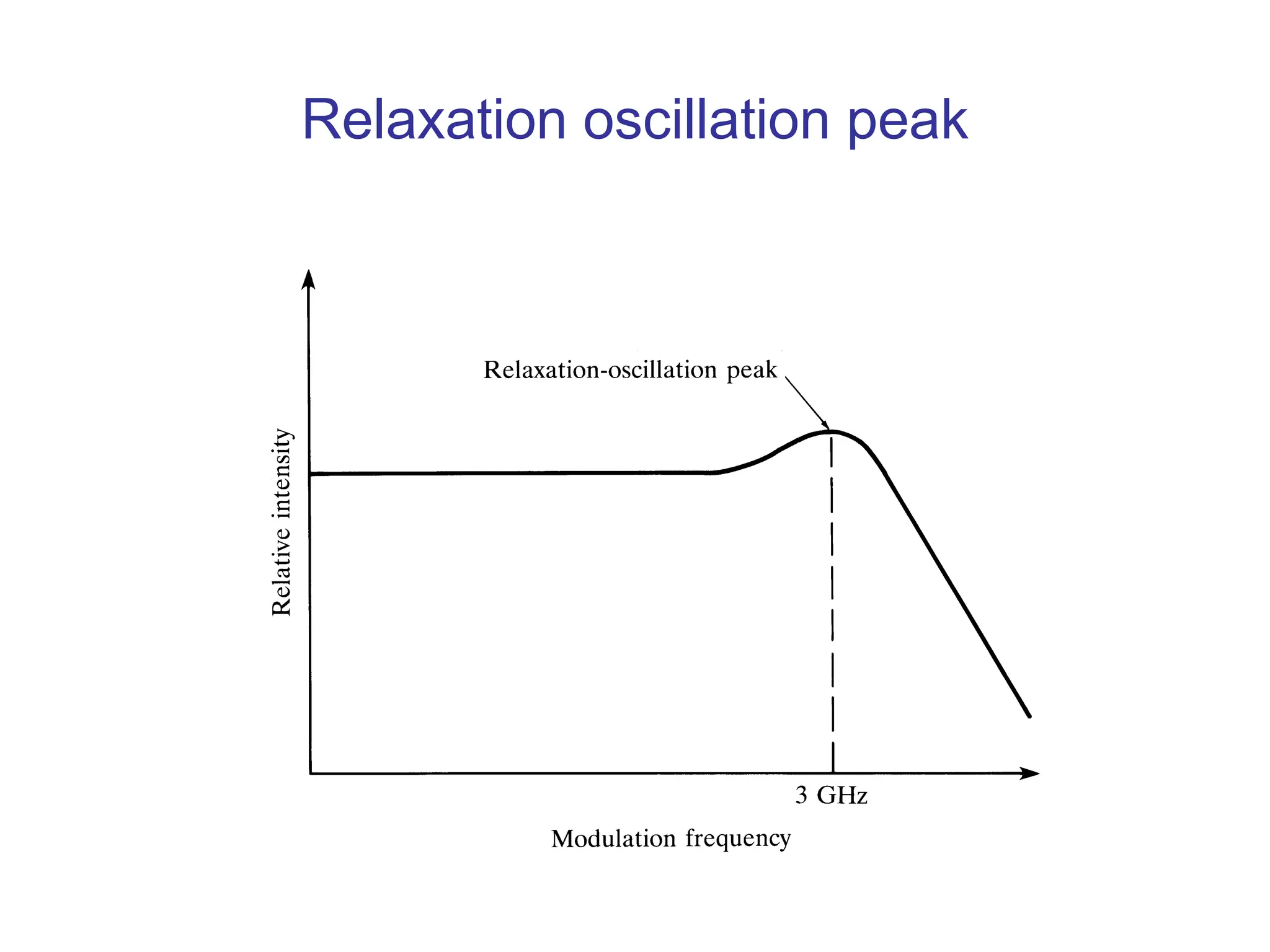
![Modulation of Laser Diodes
• Internal Modulation: Simple but suffers from non-linear effects.
• External Modulation: for rates greater than 2 Gb/s, more
complex, higher performance.
• Most fundamental limit for the modulation rate is set by the
photon life time in the laser cavity:
• Another fundamental limit on modulation frequency is the
relaxation oscillation frequency given by:
th
ph
g
n
c
R
R
L
n
c
2
1
1
ln
2
1
1
[4-36]
2
/
1
1
1
2
1
th
ph
sp
I
I
f
[4-37]](https://image.slidesharecdn.com/37-240326170031-a864a199/75/37-ocn_-ppt-Optimizing-slideshow-photodiiode-52-2048.jpg)
![Pulse Modulated laser
• In a pulse modulated laser, if the laser is completely turned off
after each pulse, after onset of the current pulse, a time delay,
given by:
d
t
)
(
ln
th
B
p
p
d
I
I
I
I
t
current
Bias
:
amplitude
pulse
Current
:
time
life
carrier
:
B
p
I
I
[4-38]](https://image.slidesharecdn.com/37-240326170031-a864a199/75/37-ocn_-ppt-Optimizing-slideshow-photodiiode-54-2048.jpg)

![Linearity of Laser
Information carrying
electrical signal s(t)
LED or Laser diode
modulator
Optical putput power:
P(t)=P[1+ms(t)]](https://image.slidesharecdn.com/37-240326170031-a864a199/75/37-ocn_-ppt-Optimizing-slideshow-photodiiode-56-2048.jpg)