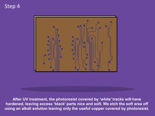
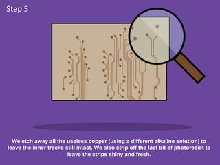
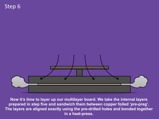
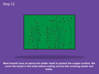
PCB Manufacturing Guide
At Hi5, we make all our PCBs with
love and care
Find out what goes on behind the scenes at
Hi5 Electronics.
You convert a board design into Gerber files and send it to us via the online
prototype shop. Our operatives will check over the design and give it initial
approval.
Step 1
We’ll create a negative image of your design so the black bits turn white and
the white bits turn black. The negative is printed on transparent film and we
punch registration holes to keep the layers aligned.
Step 2
We take a copper panel and coat it with a photosensitive film called the
photoresist. Next, we add the transparent negative film and shine a UV light
through the gaps and onto the photo-resistant copper.
Step 3
After UV treatment, the photoresist covered by ‘white’ tracks will have
hardened, leaving excess ‘black’ parts nice and soft. We etch the soft area off
using an alkali solution leaving only the useful copper covered by photoresist.
Step 4
We etch away all the useless copper (using a different alkaline solution) to
leave the inner tracks still intact. We also strip off the last bit of photoresist to
leave the strips shiny and fresh.
Step 5
Now it’s time to layer up our multilayer board. We take the internal layers
prepared in step five and sandwich them between copper foiled ‘pre-preg’.
The layers are aligned exactly using the pre-drilled holes and bonded together
in a heat-press.
Step 6
Component holes are drilled according to the Gerber files. We then ‘Black
Hole’ the pads to connect each layer of the board together, using a thin layer
of conductive film.
Step 7
Again, we laminate the outer layers with a dry photoresist. This time though,
UV light leaves the tracks and pads soft and, instead, hardens the area around
these.
Step 8
We place the board in a special bath where the tracks act as ‘attracting-
cathodes’ in the metal solution. This helps build up an extra thick layer of
electroless copper on the tracks.
Step 9
We protect the tracks with a tin edge resist . Then we etch away the
photoresist, unwanted copper and finally the tin to leave the sparkling copper
tracks.
Step 10
The boards have some time to rest while we give them a quick check over.
Step 11
Most boards have an epoxy-ink solder mask to protect the copper surface. We
cover the board in the mask before cutting out the bits covering tracks and
holes.
Step 12
We apply an immersion silver, or electroless nickel and immersion gold
(ENIG), finish over the holes. We also add a silkscreen legend to show which
component goes where.
Step 13
We ship promptly and securely.
Visit the Hi5 Electronics online shop and get a PCB made to your
specifications.

Multilayer PCB Manufacturing Process

  • 1.
    PCB Manufacturing Guide AtHi5, we make all our PCBs with love and care Find out what goes on behind the scenes at Hi5 Electronics.
  • 2.
    You convert aboard design into Gerber files and send it to us via the online prototype shop. Our operatives will check over the design and give it initial approval. Step 1
  • 3.
    We’ll create anegative image of your design so the black bits turn white and the white bits turn black. The negative is printed on transparent film and we punch registration holes to keep the layers aligned. Step 2
  • 4.
    We take acopper panel and coat it with a photosensitive film called the photoresist. Next, we add the transparent negative film and shine a UV light through the gaps and onto the photo-resistant copper. Step 3
  • 5.
    After UV treatment,the photoresist covered by ‘white’ tracks will have hardened, leaving excess ‘black’ parts nice and soft. We etch the soft area off using an alkali solution leaving only the useful copper covered by photoresist. Step 4
  • 6.
    We etch awayall the useless copper (using a different alkaline solution) to leave the inner tracks still intact. We also strip off the last bit of photoresist to leave the strips shiny and fresh. Step 5
  • 7.
    Now it’s timeto layer up our multilayer board. We take the internal layers prepared in step five and sandwich them between copper foiled ‘pre-preg’. The layers are aligned exactly using the pre-drilled holes and bonded together in a heat-press. Step 6
  • 8.
    Component holes aredrilled according to the Gerber files. We then ‘Black Hole’ the pads to connect each layer of the board together, using a thin layer of conductive film. Step 7
  • 9.
    Again, we laminatethe outer layers with a dry photoresist. This time though, UV light leaves the tracks and pads soft and, instead, hardens the area around these. Step 8
  • 10.
    We place theboard in a special bath where the tracks act as ‘attracting- cathodes’ in the metal solution. This helps build up an extra thick layer of electroless copper on the tracks. Step 9
  • 11.
    We protect thetracks with a tin edge resist . Then we etch away the photoresist, unwanted copper and finally the tin to leave the sparkling copper tracks. Step 10
  • 12.
    The boards havesome time to rest while we give them a quick check over. Step 11
  • 13.
    Most boards havean epoxy-ink solder mask to protect the copper surface. We cover the board in the mask before cutting out the bits covering tracks and holes. Step 12
  • 14.
    We apply animmersion silver, or electroless nickel and immersion gold (ENIG), finish over the holes. We also add a silkscreen legend to show which component goes where. Step 13
  • 15.
    We ship promptlyand securely. Visit the Hi5 Electronics online shop and get a PCB made to your specifications.