Downloaded 450 times
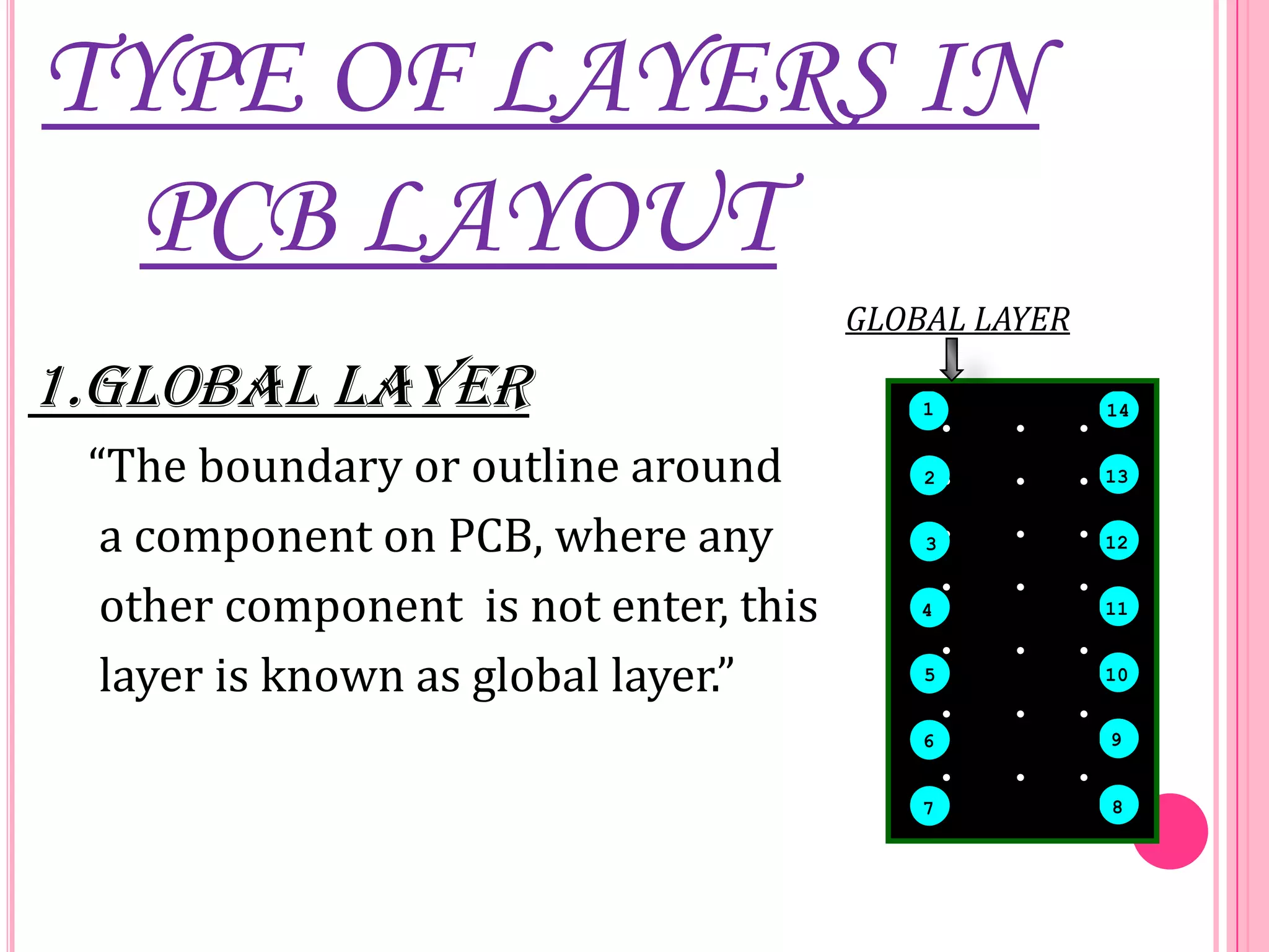
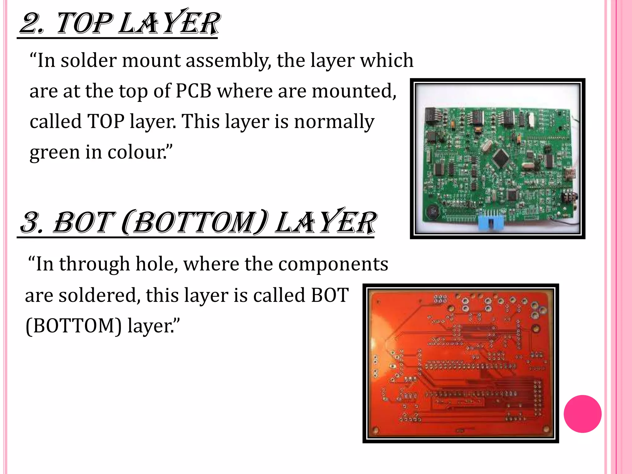
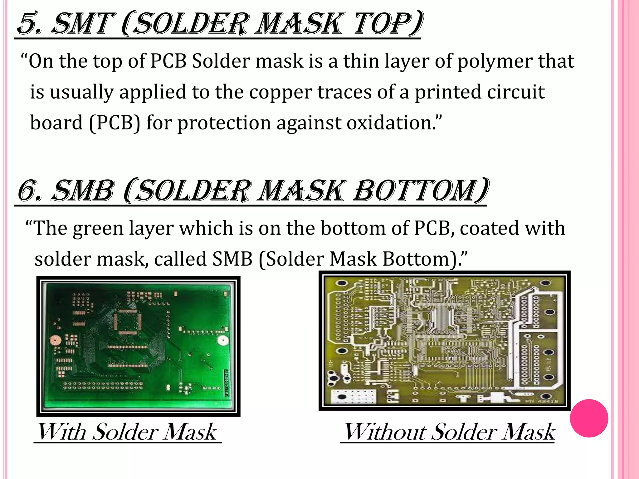
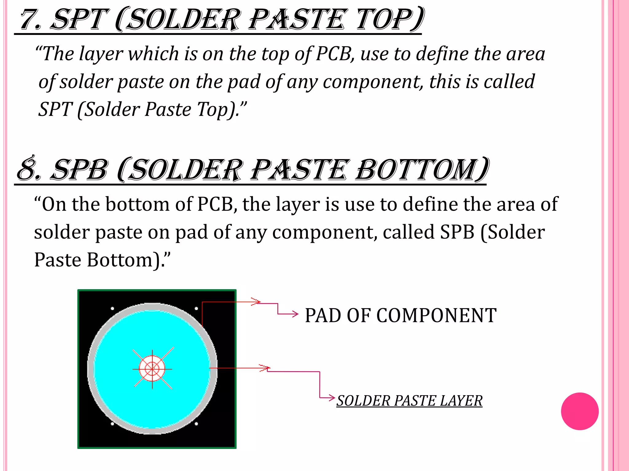
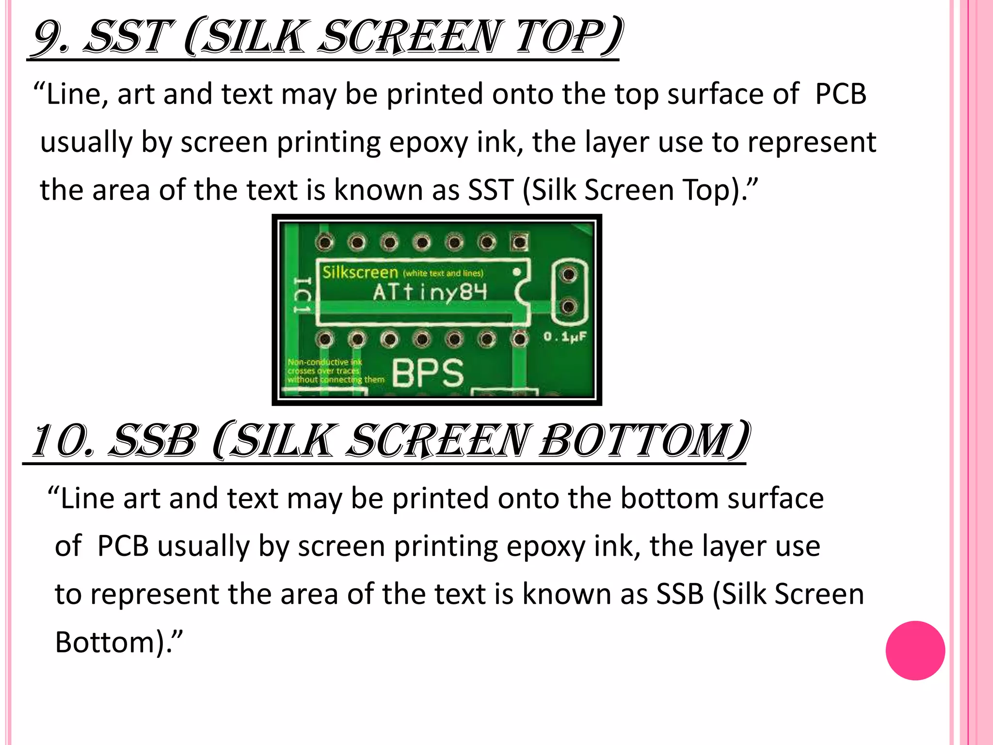
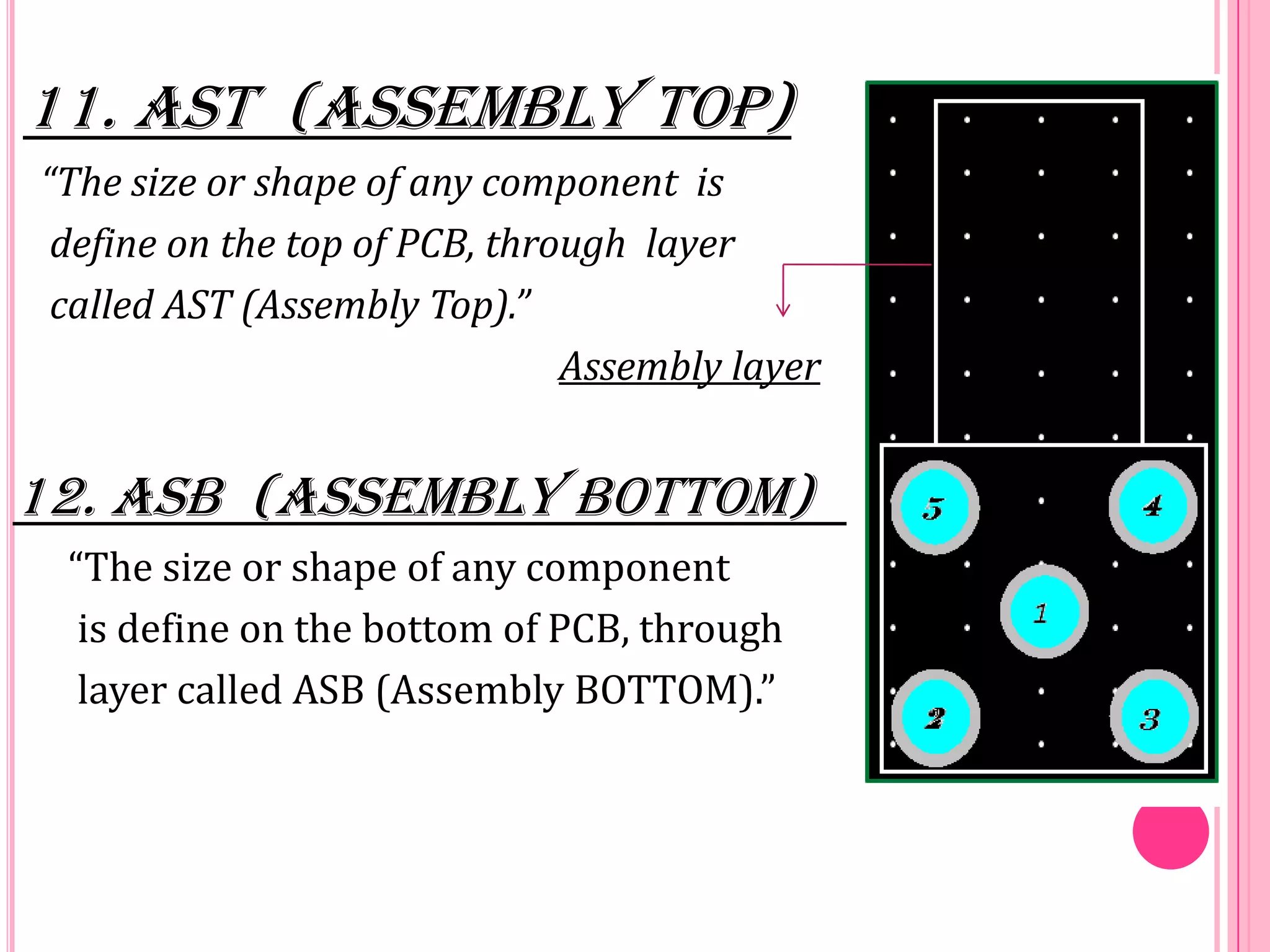
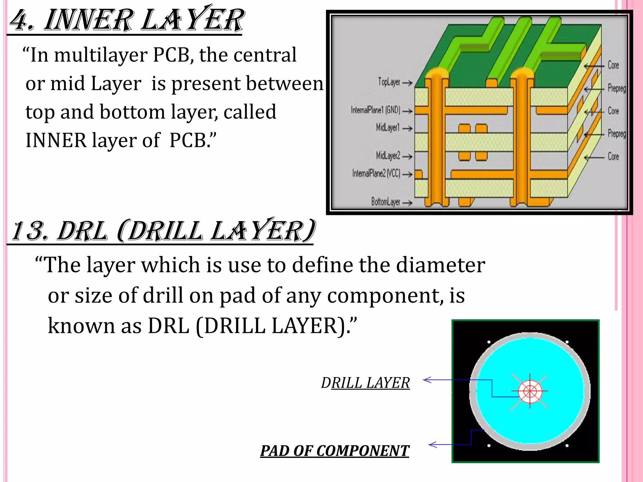

This document discusses the different types of layers used in a printed circuit board (PCB) layout. It describes 11 layers: the global layer defines component boundaries; the top and bottom layers are where components are mounted; inner layers separate top and bottom layers in multilayer PCBs; solder mask layers protect copper traces; solder paste layers define solder areas; silk screen layers contain text and markings; assembly layers define component shapes; and drill layers specify hole diameters. Each layer serves a distinct purpose in the PCB design and manufacturing process.


