Downloaded 383 times


![®
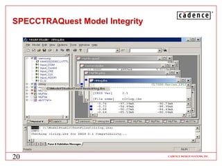
SQ Model Integrity
• Family of products that offers model creation, manipulation and
verification environment
– First release (PSD release 14.2) will offer the basic creation/editing and
sanity check environment for IO buffer models for following formats
– Cadence (DML)
– Quad [translator only]
– IBIS 3.2 [.ibs, .pkg, .ebd files]
– Future releases will offer advanced options that will provide verification
environment and handle different kinds of models
– Capacitor models for use with SPECCTRAQuest Power Integrity
– S-Parameters
– IC Package models
– Connector/FPGA models
– Link with PCB Librarian Expert series
19 CADENCE DESIGN SYSTEMS, INC.](https://image.slidesharecdn.com/high-speed-pcb-board-design-and-analysiscadence-130218085524-phpapp01/85/High-speed-pcb-board-design-and-analysis-19-320.jpg)


![®
Brief Description - Constraint Manager 14.2
• Concept Database Synchronization
Synchronizes constraints stored as Schematic properties and
CM worksheets
• Custom Measurement
Provides SigXP’s custom measurement capability in CM.
Ability to store custom measurements and to display
measurement results in CM [requires SQ SI Expert]
• Cross Probing Improvements
Cross probing with Allegro to handle segments/ratsnest, pin
pairs, DRCs and Clines
25 CADENCE DESIGN SYSTEMS, INC.](https://image.slidesharecdn.com/high-speed-pcb-board-design-and-analysiscadence-130218085524-phpapp01/85/High-speed-pcb-board-design-and-analysis-25-320.jpg)

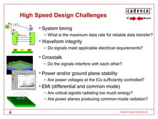
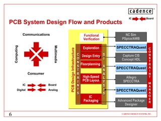
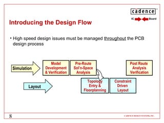
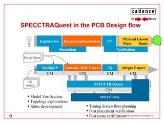
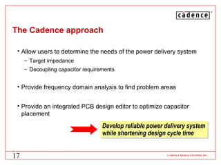
High speed PCB design faces several challenges: ensuring system timing, maintaining waveform integrity, avoiding crosstalk, and controlling power/ground stability and EMI. Cadence addresses these with a PCB design flow including functional verification, exploration, floorplanning, high-speed layout, and simulation using tools like SPECCTRAQuest and Allegro. The full flow supports both digital and analog design from IC to board.


![Signal Integrity - A Crash Course [R Lott]](https://cdn.slidesharecdn.com/ss_thumbnails/1cb0870c-cad3-4a68-ad41-8e9450fec5d8-170217191645-thumbnail.jpg?width=640&height=640&fit=bounds)