Sorry to say but the college spelling is wrong actually "technology" word is missing. Its by mistake.
A presentation on printed circuit board designing. A brief discussion on pcb fabrication. Basic steps involved in it.
Designing process of printed circuit boardselprocus
Most key element in electronic circuits and equipment’s is the Printed Circuit Board which connects electronic components with conductive lines printed
A printed circuit board (PCB) mechanically supports and electrically connects electronic components using conductive tracks, pads and other features etched from copper sheets laminated onto a non-conductive substrate.
Creative Hi-Tech would like to share some basics of Printed Circuit Boards which will help you to gain some knowledge before going to any vendor. This power point presentation will clear your basic doubts regarding the PCB.
This presentation is all about the working of Surface mount technology department of electronics industry. This is my personal experience at iljin electronics pvt. ltd. during my internship.
Step by step guide which will help to understand the PCB fabrication process. PCB manufacturing and assembly must be conducted in a clean environment that is free of contaminants. This is important to produce good quality boards that offer unfailing service for years.
Introduction to Surface Mount TechnologyABDUL MUNAFF
Surface Mount Technology (SMT) refers to a specific type of electronics assembly where electronic components are attached to the surface of a substrate (typically a printed circuit board).
SMT is a modern alternative to traditional thru-hole technology where components are attached to substrates by leads that passed through holes in the PCB.
Surface Mount components require less space so SMT is helpful in product miniaturization.
SMT Overview
SMT V/S THROUGH HOLE
Basic SMT process flow
Equipments used SMT Assembly
Through Hole Assembly & Soldering
ELECTROSTATIC DISCHARGE
RoHS
Paul Eisle was the first man to create the printed circuit board in the year 1936. However, it was in the 1950s that the US Defense Industry started integrating PCBs in the bomb detonator mechanisms. This made way for the wide application of PCBs throughout the world. These days, PCBs are widely used in almost all finished products like automobiles, personal computers and cellular telephones.
There is a ppt presentation on the process of PCB Designing . That will help others to made their own ppt in this topic. They can use it as a guidance but it is advised not to copy from this. There might be many topics that was not covered in this ppt. So, you can improve that in your own ppt
The presentation is about the heart and soul of any electronic equipment without which the engineering wont reach anywhere. Yes, I am talking about PCB which has made the dream come true.
PCBA is the abbreviation of Printed Circuit Board Assembly, which means that the PCB blank board passes the SMT upper part, or the whole process of DIP plug-in, referred to as PCBA.
Importance of PCB assembly in Various Industries | Suntronic Inc |SuntronicInc
PCB assembly is crucial across industries for integrating electronic components into functional systems. In consumer electronics, it enables compact designs and mass production of devices like smartphones. In automotive, it powers vital systems like ECUs and infotainment. In aerospace and defense, it ensures reliability in avionics and radar systems. Healthcare relies on it for precise medical devices, and industrial automation benefits from efficient control systems. Overall, PCB assembly drives innovation, reliability, and efficiency across diverse sectors
Suntronic is a leading Electronics Manufacturing Services (EMS) provider with facilities in Houston and Dallas focused on delivering design and manufacturing services to Oil and Gas, industrial controls, communications, infrastructure, and OEM’s. Founded in 1995, we base our business off of the fundamentals of providing highest quality, exceptional customer services, state of the art equipment and technical expertise.
At Suntronic we offer full-range manufacturing services which include quick-turn 24-hour prototype, pilot-run/pre-production to full production printed circuit board assemblies, complex system level assembly/integration, test services, cable & wire harness assemblies, and box builds. Our expertise in complex designs for mission critical environments helps us drive the success of the clients we serve.
TECHNICAL TRAINING MANUAL GENERAL FAMILIARIZATION COURSEDuvanRamosGarzon1
AIRCRAFT GENERAL
The Single Aisle is the most advanced family aircraft in service today, with fly-by-wire flight controls.
The A318, A319, A320 and A321 are twin-engine subsonic medium range aircraft.
The family offers a choice of engines
Saudi Arabia stands as a titan in the global energy landscape, renowned for its abundant oil and gas resources. It's the largest exporter of petroleum and holds some of the world's most significant reserves. Let's delve into the top 10 oil and gas projects shaping Saudi Arabia's energy future in 2024.
Forklift Classes Overview by Intella PartsIntella Parts
Discover the different forklift classes and their specific applications. Learn how to choose the right forklift for your needs to ensure safety, efficiency, and compliance in your operations.
For more technical information, visit our website https://intellaparts.com
NO1 Uk best vashikaran specialist in delhi vashikaran baba near me online vas...Amil Baba Dawood bangali
Contact with Dawood Bhai Just call on +92322-6382012 and we'll help you. We'll solve all your problems within 12 to 24 hours and with 101% guarantee and with astrology systematic. If you want to take any personal or professional advice then also you can call us on +92322-6382012 , ONLINE LOVE PROBLEM & Other all types of Daily Life Problem's.Then CALL or WHATSAPP us on +92322-6382012 and Get all these problems solutions here by Amil Baba DAWOOD BANGALI
#vashikaranspecialist #astrologer #palmistry #amliyaat #taweez #manpasandshadi #horoscope #spiritual #lovelife #lovespell #marriagespell#aamilbabainpakistan #amilbabainkarachi #powerfullblackmagicspell #kalajadumantarspecialist #realamilbaba #AmilbabainPakistan #astrologerincanada #astrologerindubai #lovespellsmaster #kalajaduspecialist #lovespellsthatwork #aamilbabainlahore#blackmagicformarriage #aamilbaba #kalajadu #kalailam #taweez #wazifaexpert #jadumantar #vashikaranspecialist #astrologer #palmistry #amliyaat #taweez #manpasandshadi #horoscope #spiritual #lovelife #lovespell #marriagespell#aamilbabainpakistan #amilbabainkarachi #powerfullblackmagicspell #kalajadumantarspecialist #realamilbaba #AmilbabainPakistan #astrologerincanada #astrologerindubai #lovespellsmaster #kalajaduspecialist #lovespellsthatwork #aamilbabainlahore #blackmagicforlove #blackmagicformarriage #aamilbaba #kalajadu #kalailam #taweez #wazifaexpert #jadumantar #vashikaranspecialist #astrologer #palmistry #amliyaat #taweez #manpasandshadi #horoscope #spiritual #lovelife #lovespell #marriagespell#aamilbabainpakistan #amilbabainkarachi #powerfullblackmagicspell #kalajadumantarspecialist #realamilbaba #AmilbabainPakistan #astrologerincanada #astrologerindubai #lovespellsmaster #kalajaduspecialist #lovespellsthatwork #aamilbabainlahore #Amilbabainuk #amilbabainspain #amilbabaindubai #Amilbabainnorway #amilbabainkrachi #amilbabainlahore #amilbabaingujranwalan #amilbabainislamabad
Automobile Management System Project Report.pdfKamal Acharya
The proposed project is developed to manage the automobile in the automobile dealer company. The main module in this project is login, automobile management, customer management, sales, complaints and reports. The first module is the login. The automobile showroom owner should login to the project for usage. The username and password are verified and if it is correct, next form opens. If the username and password are not correct, it shows the error message.
When a customer search for a automobile, if the automobile is available, they will be taken to a page that shows the details of the automobile including automobile name, automobile ID, quantity, price etc. “Automobile Management System” is useful for maintaining automobiles, customers effectively and hence helps for establishing good relation between customer and automobile organization. It contains various customized modules for effectively maintaining automobiles and stock information accurately and safely.
When the automobile is sold to the customer, stock will be reduced automatically. When a new purchase is made, stock will be increased automatically. While selecting automobiles for sale, the proposed software will automatically check for total number of available stock of that particular item, if the total stock of that particular item is less than 5, software will notify the user to purchase the particular item.
Also when the user tries to sale items which are not in stock, the system will prompt the user that the stock is not enough. Customers of this system can search for a automobile; can purchase a automobile easily by selecting fast. On the other hand the stock of automobiles can be maintained perfectly by the automobile shop manager overcoming the drawbacks of existing system.
Water scarcity is the lack of fresh water resources to meet the standard water demand. There are two type of water scarcity. One is physical. The other is economic water scarcity.
Immunizing Image Classifiers Against Localized Adversary Attacksgerogepatton
This paper addresses the vulnerability of deep learning models, particularly convolutional neural networks
(CNN)s, to adversarial attacks and presents a proactive training technique designed to counter them. We
introduce a novel volumization algorithm, which transforms 2D images into 3D volumetric representations.
When combined with 3D convolution and deep curriculum learning optimization (CLO), itsignificantly improves
the immunity of models against localized universal attacks by up to 40%. We evaluate our proposed approach
using contemporary CNN architectures and the modified Canadian Institute for Advanced Research (CIFAR-10
and CIFAR-100) and ImageNet Large Scale Visual Recognition Challenge (ILSVRC12) datasets, showcasing
accuracy improvements over previous techniques. The results indicate that the combination of the volumetric
input and curriculum learning holds significant promise for mitigating adversarial attacks without necessitating
adversary training.
Student information management system project report ii.pdfKamal Acharya
Our project explains about the student management. This project mainly explains the various actions related to student details. This project shows some ease in adding, editing and deleting the student details. It also provides a less time consuming process for viewing, adding, editing and deleting the marks of the students.
Final project report on grocery store management system..pdfKamal Acharya
In today’s fast-changing business environment, it’s extremely important to be able to respond to client needs in the most effective and timely manner. If your customers wish to see your business online and have instant access to your products or services.
Online Grocery Store is an e-commerce website, which retails various grocery products. This project allows viewing various products available enables registered users to purchase desired products instantly using Paytm, UPI payment processor (Instant Pay) and also can place order by using Cash on Delivery (Pay Later) option. This project provides an easy access to Administrators and Managers to view orders placed using Pay Later and Instant Pay options.
In order to develop an e-commerce website, a number of Technologies must be studied and understood. These include multi-tiered architecture, server and client-side scripting techniques, implementation technologies, programming language (such as PHP, HTML, CSS, JavaScript) and MySQL relational databases. This is a project with the objective to develop a basic website where a consumer is provided with a shopping cart website and also to know about the technologies used to develop such a website.
This document will discuss each of the underlying technologies to create and implement an e- commerce website.
Event Management System Vb Net Project Report.pdfKamal Acharya
In present era, the scopes of information technology growing with a very fast .We do not see any are untouched from this industry. The scope of information technology has become wider includes: Business and industry. Household Business, Communication, Education, Entertainment, Science, Medicine, Engineering, Distance Learning, Weather Forecasting. Carrier Searching and so on.
My project named “Event Management System” is software that store and maintained all events coordinated in college. It also helpful to print related reports. My project will help to record the events coordinated by faculties with their Name, Event subject, date & details in an efficient & effective ways.
In my system we have to make a system by which a user can record all events coordinated by a particular faculty. In our proposed system some more featured are added which differs it from the existing system such as security.
COLLEGE BUS MANAGEMENT SYSTEM PROJECT REPORT.pdfKamal Acharya
The College Bus Management system is completely developed by Visual Basic .NET Version. The application is connect with most secured database language MS SQL Server. The application is develop by using best combination of front-end and back-end languages. The application is totally design like flat user interface. This flat user interface is more attractive user interface in 2017. The application is gives more important to the system functionality. The application is to manage the student’s details, driver’s details, bus details, bus route details, bus fees details and more. The application has only one unit for admin. The admin can manage the entire application. The admin can login into the application by using username and password of the admin. The application is develop for big and small colleges. It is more user friendly for non-computer person. Even they can easily learn how to manage the application within hours. The application is more secure by the admin. The system will give an effective output for the VB.Net and SQL Server given as input to the system. The compiled java program given as input to the system, after scanning the program will generate different reports. The application generates the report for users. The admin can view and download the report of the data. The application deliver the excel format reports. Because, excel formatted reports is very easy to understand the income and expense of the college bus. This application is mainly develop for windows operating system users. In 2017, 73% of people enterprises are using windows operating system. So the application will easily install for all the windows operating system users. The application-developed size is very low. The application consumes very low space in disk. Therefore, the user can allocate very minimum local disk space for this application.
Vaccine management system project report documentation..pdfKamal Acharya
The Division of Vaccine and Immunization is facing increasing difficulty monitoring vaccines and other commodities distribution once they have been distributed from the national stores. With the introduction of new vaccines, more challenges have been anticipated with this additions posing serious threat to the already over strained vaccine supply chain system in Kenya.
Hybrid optimization of pumped hydro system and solar- Engr. Abdul-Azeez.pdffxintegritypublishin
Advancements in technology unveil a myriad of electrical and electronic breakthroughs geared towards efficiently harnessing limited resources to meet human energy demands. The optimization of hybrid solar PV panels and pumped hydro energy supply systems plays a pivotal role in utilizing natural resources effectively. This initiative not only benefits humanity but also fosters environmental sustainability. The study investigated the design optimization of these hybrid systems, focusing on understanding solar radiation patterns, identifying geographical influences on solar radiation, formulating a mathematical model for system optimization, and determining the optimal configuration of PV panels and pumped hydro storage. Through a comparative analysis approach and eight weeks of data collection, the study addressed key research questions related to solar radiation patterns and optimal system design. The findings highlighted regions with heightened solar radiation levels, showcasing substantial potential for power generation and emphasizing the system's efficiency. Optimizing system design significantly boosted power generation, promoted renewable energy utilization, and enhanced energy storage capacity. The study underscored the benefits of optimizing hybrid solar PV panels and pumped hydro energy supply systems for sustainable energy usage. Optimizing the design of solar PV panels and pumped hydro energy supply systems as examined across diverse climatic conditions in a developing country, not only enhances power generation but also improves the integration of renewable energy sources and boosts energy storage capacities, particularly beneficial for less economically prosperous regions. Additionally, the study provides valuable insights for advancing energy research in economically viable areas. Recommendations included conducting site-specific assessments, utilizing advanced modeling tools, implementing regular maintenance protocols, and enhancing communication among system components.
Hybrid optimization of pumped hydro system and solar- Engr. Abdul-Azeez.pdf
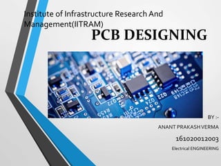
PCB Designing
1. PCB DESIGNING
BY :-
ANANT PRAKASHVERMA
161020012003
Electrical ENGINEERING
Institute of Infrastructure Research And
Management(IITRAM)
2. History of Printed Circuit Board
• First working device to use a printed circuit board (PCB) was
radio, invented by Paul Eisler. in 1942.
• First double sided PCB were produced in 1947.
• In 1960 multi layer-production began (4+ layer)
• In 2010 PCB production became multi-billion dollar market.
3. Introduction to a Printed Circuit Board
• A printed circuit board (PCB) :mechanically supports and electrically
connects, electronic components using conductive tracks, pads and other
features etched from copper sheets laminated onto a non-
conductive substrate. Components are generally soldered on PCB.
• PCB's can be single sided (one copper layer), double sided (two copper
layers) or multi-layer.
• A PCB populated with electronic components is called a printed circuit
assembly (PCA), printed circuit board assembly or PCB assembly (PCBA)
• Manufacturing circuit with PCB
is cheaper and faster.
4. What PCB is made of
• A basic PCB starts with a copper-clad fiberglass material
or thin copper sheets attached to either side of the board. It
consist of :-
Copper Foil
Copper Plating
Solder Flow
Solder Mask
Trace
Slots and Cut-outs
5. PCB CHARACTERISTICS
• Through-hole technology
The first PCBs used through-hole technology, mounting electronic
components by leads inserted through holes on one side of the board
and soldered onto copper traces on the other side. Boards may be
single-sided, with an un plated component side, or more compact
double-sided boards, with components soldered on both sides
6. PCB CHARACTERISTICS (cont.)
•Surface-mount technology
Surface-mount technology emerged in the 1960s, gained
momentum in the early 1980s and became widely used by the mid-
1990s. Components were mechanically redesigned to have small
metal tabs or end caps that could be soldered directly onto the PCB
surface, instead of wire leads to pass through holes
7. FABRICATION
Following are the basic steps of PCB design.
• Imaging
• Panelization
• Depaneling
• Etching
• Drilling
• Assembly
• Electrical Test
8. FABRICATION (cont.)
• Imaging : before manufacturing the
PCB fabrication data is generated by
computer aided design(CAD),
such as Siemens-NX, Autodesk, etc.
This data is read into the CAM(Computer Aided Manufacturing)
9. FABRICATION (cont.)
• Panelization : It’s a procedure whereby a number of PCBs
grouped for manufacturing onto a larger board(panel). There
are two type of panels
1. Assembly panel
2.Bare- Board manufacturing panel
10. FABRICATION (cont.)
• Depaneling: The panel is eventually broken into individual
PCBs. Its done by lasers it cuts the panel and reduce stress on
circuit board
• Copper Patterning : This step is to replicated the pattern on
copper foil. Subsequent etching removes the unwanted copper.
Some of the technique used for hybrid circuit.
1. Silk screen printing .
2. Photoengraving .
3. PCB milling .
4. CNC laser plotter.
11. FABRICATION (cont.)
Etching process
Chemical etch
• Chemical etching is usually done with
ammonium per sulphate or ferric chloride.
• For PTH (plated-through holes), additional steps of electroless
deposition are done after the holes are drilled, then copper is
electroplated to build up the thickness, the boards are screened,
and plated with tin/lead. The tin/lead becomes the resist leaving
the bare copper to be etched away.
Cont.…
12. FABRICATION (cont.)
Laser Etch
• A new process creating new standards and the demise of the
chemical process is plasma etch. In addition to no etch-back,
this process also eliminates imaging, or film error using a
direct imaging process, which transfers the layer image directly
to the material
13. FABRICATION (cont.)
• Drilling: Holes through a PCB are typically drilled with small
diameter drill bits made of tungsten carbide. Drilling is generally
performed by automated drilling machines.
• Assembly: In this step the board is
filled with electronic component ,using
variety of soldering techniques this is
known as printed circuit board assembly
(PCBA).
14. Industry Applications of PCB
• Automotive Industry
• Medical Industry
• Defence
• Scientific Instrumentation
• Broadcasting
• Power management
• Retail Industry
….etc.
15. Power supply board
• A power supply is a device that supplies electric power to
an electrical load.
• Power converters that convert one form of electrical energy
to another.
• Power supplies for electronic devices can be broadly divided
into two type
1. Linear power supplies
2. Switching power supplies.
16. Power supply board (contd.)
• Linear power supplies:
Linear power converters process the input power directly, with all
active power conversion components operating in their linear
operating regions. Example our power meter.
• Switching power supplies:
The input power is converted to AC or to DC pulses before
processing, by components that operate predominantly in non-
linear modes (e.g., transistors)