Downloaded 1,571 times
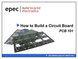

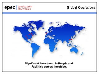
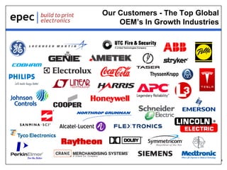


The document outlines the history and capabilities of a privately held company that specializes in designing and manufacturing printed circuit boards (PCBs) and related products since 1952. It details the PCB construction process, including materials, design considerations, manufacturing techniques, and quality testing protocols. The company serves top global OEMs in various electronics sectors, emphasizing the importance of effective supply chain and manufacturing strategies.


