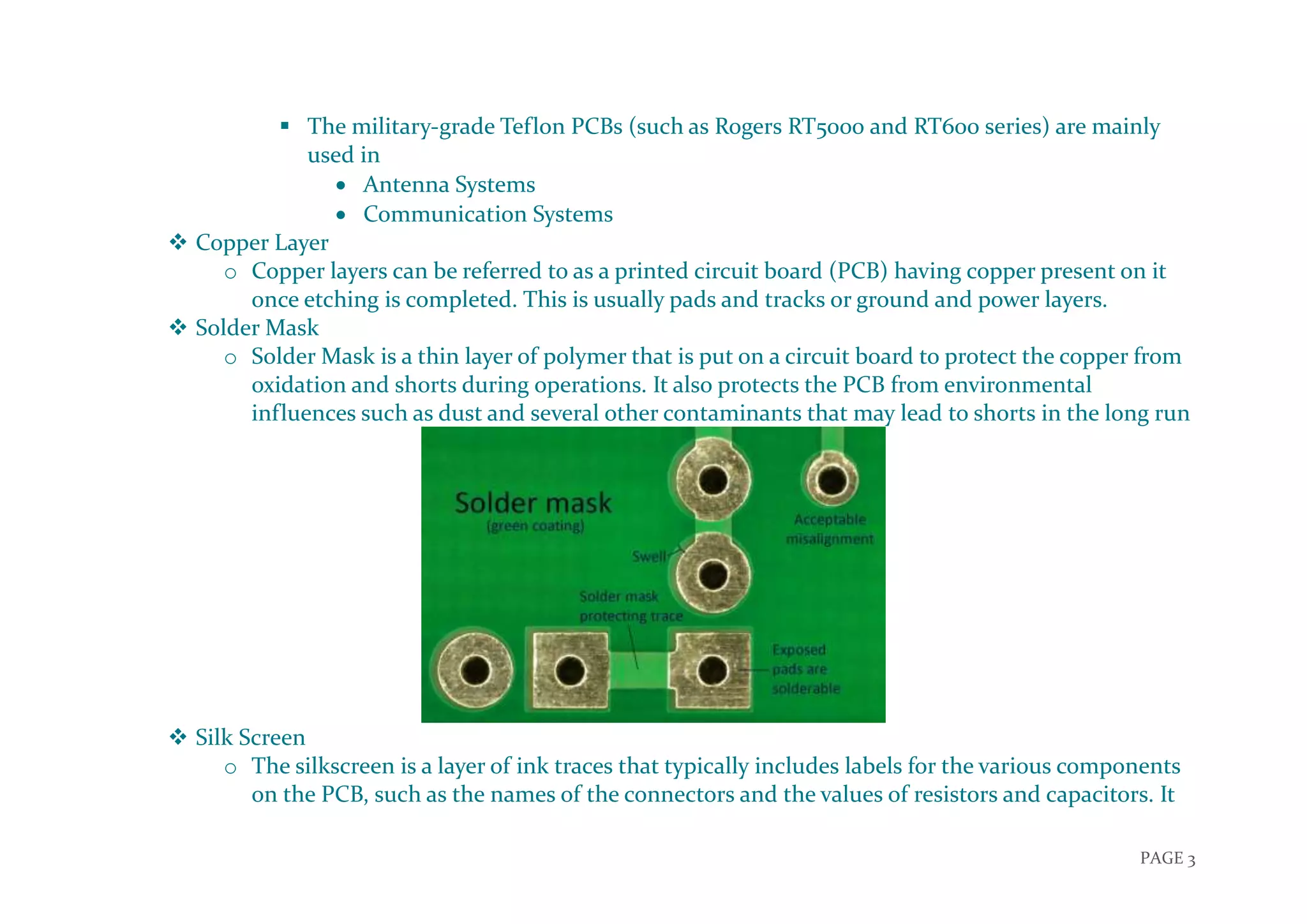
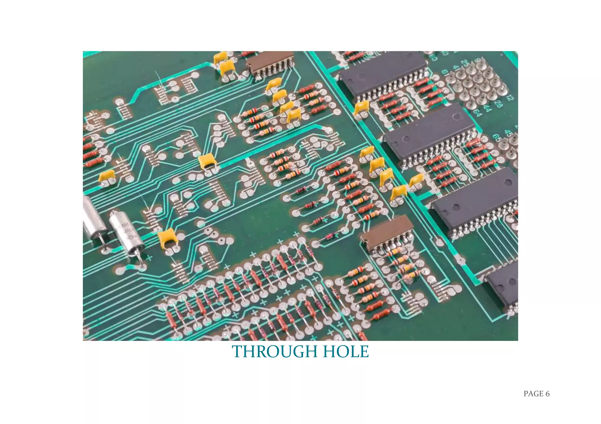
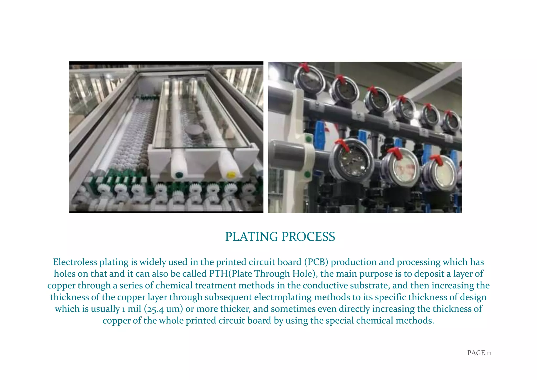
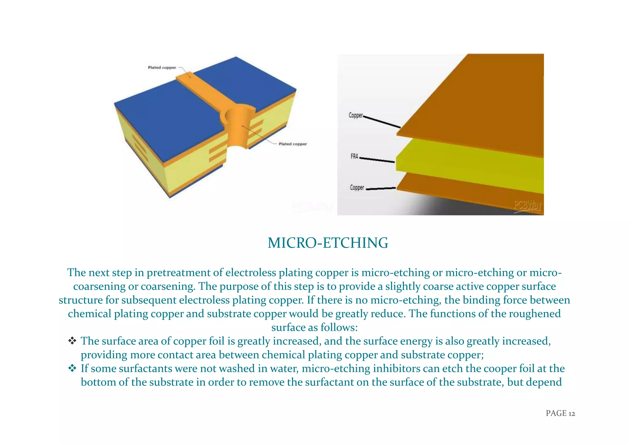
The document discusses the PCB manufacturing process. It describes what a PCB is and the different types of PCBs. It then explains the key layers that make up a PCB, including the substrate, copper layers, solder mask, and silkscreen. The document proceeds to outline several stages of the PCB manufacturing process, including PCB drilling, film development, etching, plating, micro-etching. The overall process produces circuit boards by applying conductive traces to a non-conductive substrate.
These processes are sometimes referred to as post-processing. They play a very important role in the appearance, function and life of the product. Broadly, these are processes that affect either a thin layer on the surface of the part itself, or add a thin layer on top of the surface of the part. There are different coating and surface treatments processes, with different applications, uses, etc. The important uses include:
• Improving the hardness
• Improving the wear resistance
• Controlling friction, Reduction of adhesion, improving the lubrication, etc.
• Improving corrosion resistance
• Improving aesthetics
9.1. Mechanical hardening of the surface
These methods apply mechanical impulses (e.g. light hammering) on the surface of a metallic part. This hammering action causes tiny amount of plastic flow on the surface, resulting in the work-hardening of the surface layer due to the introduction of compressive residual stresses. Examples of these processes include Shot peening (uses tiny balls of metal or ceramic), Water-jet peening (uses a jet of water at high pressures, e.g. 400 MPa), or Laser peening (surface is hit by tiny impulses from a laser) – an expensive process used to improve fatigue strength of jet fan blades and turbine impellers.
Another method is explosive hardening, where a layer of explosive coated on the surface is blasted – the resulting impact results in tremendous increase in the surface hardness. This method is used to harden the surface of train rails.
9.2. Case hardening
This is a very common process that is used to harden the outer surface of parts such as gear teeth, cams, shafts, bearings, fasteners, pins, tools, molds, dies etc. In most of these types of components, the use involves dynamic forces, occasional impacts, and constant friction. Therefore the surface needs to be hard to prevent wear, but the bulk of the part should be tough (not brittle); this is achieved best by case hardening. There are several types of case hardening: in most cases, the chemical structure of the metal is changed by diffusing atoms of an alternate element which results in alterations to the micro-structure on the crystals on the surface.
Paul Ahern - Copper/ low-K Interconnect TechnologyPaul Ahern
The one hallmark that typifies the evolution of integrated circuit technology is the relentless move towards faster clock speeds and smaller geometries. The foremost test facing chipmakers today is how to continue to drive this process forward, extending Moore’s Law in the face of fundamental obstacles. The two areas which are providing the biggest hurdles to IC manufacturing today (1) are trying to scale lithography, and (2) scaling interconnect technology into the sub-22 nanometer range.
This term presentation was submitted as a partial requirement for the course: MSE 507: Advanced micro-fabrication with CAD (TSUPREM4). In this presentation, the fabrication process of 3D FINFET transistor has been presented in accordance with US patent (Patent no. US 7,973,389 B2, assignee: Intel Corporation, Santa Clara, CA, US) using Shallow Trench Isolation (STI) method.
Canada Metal: Lead sheet metal for nuclear shielding, Constructioncanadametal
Canada Metal supplies lead sheet metal for multiple purposes like radiation shielding, nuclear shielding or construction and many more uses. Canada Metal provides high quality sheet lead with many type of thickness on cost effective range. http://www.canadametal.com/products/lead/sheet-lead/
First, the PCB board concept
PCB board is also known as the printed circuit board, is an important electronic component, is the support body of electronic components, is the provider of electrical connection of electronic components. As it is made using electronic printing, it is called a "printed" circuit board.
A printed circuit board(PCB) is a laminated sandwich structure of conductive and insulating layers.
Multi Layer Printed Circuit Board Introduction and Manufacturing processAditya Deshpande
Multi Layer Printed Circuit Board Introduction and Manufacturing process presentation will help you to understand how the miniaturization is possible in electronics and also the Manufacturing of Multi Layer Printed Circuit Board.
What is CAF?
A growth consisting of a conductive copper-containing salt. It is created electrochemically and grows from the anode toward the cathode subsurface along the epoxy/glass interface.
Conductive Anodic Filament (CAF) formation does happen
o When it happens, it can cause a lot of pain
CAF behavior is relatively stable
o Limited change in key PCB technology (pitch, materials,
assembly)
CAF mitigation is well known (execute it!)
o Evaluate your designs
o Qualify your suppliers
Hybrid optimization of pumped hydro system and solar- Engr. Abdul-Azeez.pdffxintegritypublishin
Advancements in technology unveil a myriad of electrical and electronic breakthroughs geared towards efficiently harnessing limited resources to meet human energy demands. The optimization of hybrid solar PV panels and pumped hydro energy supply systems plays a pivotal role in utilizing natural resources effectively. This initiative not only benefits humanity but also fosters environmental sustainability. The study investigated the design optimization of these hybrid systems, focusing on understanding solar radiation patterns, identifying geographical influences on solar radiation, formulating a mathematical model for system optimization, and determining the optimal configuration of PV panels and pumped hydro storage. Through a comparative analysis approach and eight weeks of data collection, the study addressed key research questions related to solar radiation patterns and optimal system design. The findings highlighted regions with heightened solar radiation levels, showcasing substantial potential for power generation and emphasizing the system's efficiency. Optimizing system design significantly boosted power generation, promoted renewable energy utilization, and enhanced energy storage capacity. The study underscored the benefits of optimizing hybrid solar PV panels and pumped hydro energy supply systems for sustainable energy usage. Optimizing the design of solar PV panels and pumped hydro energy supply systems as examined across diverse climatic conditions in a developing country, not only enhances power generation but also improves the integration of renewable energy sources and boosts energy storage capacities, particularly beneficial for less economically prosperous regions. Additionally, the study provides valuable insights for advancing energy research in economically viable areas. Recommendations included conducting site-specific assessments, utilizing advanced modeling tools, implementing regular maintenance protocols, and enhancing communication among system components.
TECHNICAL TRAINING MANUAL GENERAL FAMILIARIZATION COURSEDuvanRamosGarzon1
AIRCRAFT GENERAL
The Single Aisle is the most advanced family aircraft in service today, with fly-by-wire flight controls.
The A318, A319, A320 and A321 are twin-engine subsonic medium range aircraft.
The family offers a choice of engines
Automobile Management System Project Report.pdfKamal Acharya
The proposed project is developed to manage the automobile in the automobile dealer company. The main module in this project is login, automobile management, customer management, sales, complaints and reports. The first module is the login. The automobile showroom owner should login to the project for usage. The username and password are verified and if it is correct, next form opens. If the username and password are not correct, it shows the error message.
When a customer search for a automobile, if the automobile is available, they will be taken to a page that shows the details of the automobile including automobile name, automobile ID, quantity, price etc. “Automobile Management System” is useful for maintaining automobiles, customers effectively and hence helps for establishing good relation between customer and automobile organization. It contains various customized modules for effectively maintaining automobiles and stock information accurately and safely.
When the automobile is sold to the customer, stock will be reduced automatically. When a new purchase is made, stock will be increased automatically. While selecting automobiles for sale, the proposed software will automatically check for total number of available stock of that particular item, if the total stock of that particular item is less than 5, software will notify the user to purchase the particular item.
Also when the user tries to sale items which are not in stock, the system will prompt the user that the stock is not enough. Customers of this system can search for a automobile; can purchase a automobile easily by selecting fast. On the other hand the stock of automobiles can be maintained perfectly by the automobile shop manager overcoming the drawbacks of existing system.
Final project report on grocery store management system..pdfKamal Acharya
In today’s fast-changing business environment, it’s extremely important to be able to respond to client needs in the most effective and timely manner. If your customers wish to see your business online and have instant access to your products or services.
Online Grocery Store is an e-commerce website, which retails various grocery products. This project allows viewing various products available enables registered users to purchase desired products instantly using Paytm, UPI payment processor (Instant Pay) and also can place order by using Cash on Delivery (Pay Later) option. This project provides an easy access to Administrators and Managers to view orders placed using Pay Later and Instant Pay options.
In order to develop an e-commerce website, a number of Technologies must be studied and understood. These include multi-tiered architecture, server and client-side scripting techniques, implementation technologies, programming language (such as PHP, HTML, CSS, JavaScript) and MySQL relational databases. This is a project with the objective to develop a basic website where a consumer is provided with a shopping cart website and also to know about the technologies used to develop such a website.
This document will discuss each of the underlying technologies to create and implement an e- commerce website.
Courier management system project report.pdfKamal Acharya
It is now-a-days very important for the people to send or receive articles like imported furniture, electronic items, gifts, business goods and the like. People depend vastly on different transport systems which mostly use the manual way of receiving and delivering the articles. There is no way to track the articles till they are received and there is no way to let the customer know what happened in transit, once he booked some articles. In such a situation, we need a system which completely computerizes the cargo activities including time to time tracking of the articles sent. This need is fulfilled by Courier Management System software which is online software for the cargo management people that enables them to receive the goods from a source and send them to a required destination and track their status from time to time.
Quality defects in TMT Bars, Possible causes and Potential Solutions.PrashantGoswami42
Maintaining high-quality standards in the production of TMT bars is crucial for ensuring structural integrity in construction. Addressing common defects through careful monitoring, standardized processes, and advanced technology can significantly improve the quality of TMT bars. Continuous training and adherence to quality control measures will also play a pivotal role in minimizing these defects.
Event Management System Vb Net Project Report.pdfKamal Acharya
In present era, the scopes of information technology growing with a very fast .We do not see any are untouched from this industry. The scope of information technology has become wider includes: Business and industry. Household Business, Communication, Education, Entertainment, Science, Medicine, Engineering, Distance Learning, Weather Forecasting. Carrier Searching and so on.
My project named “Event Management System” is software that store and maintained all events coordinated in college. It also helpful to print related reports. My project will help to record the events coordinated by faculties with their Name, Event subject, date & details in an efficient & effective ways.
In my system we have to make a system by which a user can record all events coordinated by a particular faculty. In our proposed system some more featured are added which differs it from the existing system such as security.
Vaccine management system project report documentation..pdfKamal Acharya
The Division of Vaccine and Immunization is facing increasing difficulty monitoring vaccines and other commodities distribution once they have been distributed from the national stores. With the introduction of new vaccines, more challenges have been anticipated with this additions posing serious threat to the already over strained vaccine supply chain system in Kenya.
Water scarcity is the lack of fresh water resources to meet the standard water demand. There are two type of water scarcity. One is physical. The other is economic water scarcity.
2. PAGE 1
What is a PCB?
1. A PCB is a flat board made of non-conductive material, usually fiber glass or composite glass epoxy, on
which electronic components are mounted.
2. A PCB can have conductors on one side or two sides and can be multi-layered sandwich with many
layers of conductors, each separated by insulating layers.
3. They provide a compact and organized platform for connecting and mounting components,
simplifying the assembly process.
Types of PCB
Single Side
Double Side
Multilayer
Rigid-flex
Layers of a PCB
Substrate
o FR-4
FR4 is a class of printed circuit board base material made from a flame retardant epoxy
resin and glass fabric composite. FR stands for flame retardant and meets the
requirements of UL94V-0. FR4 has good adhesion to copper foil and has minimal water
absorption, making it very suitable for standard applications. FR4 is either used as a
copper-coated material for 1 and 2-layer PCBs or is used for multilayer PCBs
3. PAGE 2
o Teflon
PTFE Teflon PCB to meet the demand for faster communications. Teflon materials are
valued for their suitability in high-frequency electronic applications. The most common
of these Teflon PCB materials were developed by Rogers.
4. PAGE 3
The military-grade Teflon PCBs (such as Rogers RT5000 and RT600 series) are mainly
used in
Antenna Systems
Communication Systems
Copper Layer
o Copper layers can be referred to as a printed circuit board (PCB) having copper present on it
once etching is completed. This is usually pads and tracks or ground and power layers.
Solder Mask
o Solder Mask is a thin layer of polymer that is put on a circuit board to protect the copper from
oxidation and shorts during operations. It also protects the PCB from environmental
influences such as dust and several other contaminants that may lead to shorts in the long run
Silk Screen
o The silkscreen is a layer of ink traces that typically includes labels for the various components
on the PCB, such as the names of the connectors and the values of resistors and capacitors. It
5. PAGE 4
may also include other information, such as the PCB's title, the polarity of parts, and the test
point locations. The silkscreen is applied to the component part of the printed circuit board.
LEGEND
9. PAGE 8
PCB DRILLING
PCB drilling (which is also known as printed circuit board drilling), is the process of creating holes,
slots and other cavities in an electronic circuit board.
Drilling is the most expensive and time-consuming part of the circuit board manufacturing process.
This is because the process must be carried out exactly to ensure the highest possible levels of quality.
After the substrate has been prepared for drilling, tooling pins are inserted and are used to hold the
board while it’s in the pre-programmed computer numerically controlled (CNC) machine. Then, the
component mounting holes are drilled in the PCB before the boards are split and measured for
accuracy.
Finally, a polisher scrubs the surface of the copper clean to remove any small burrs or rough edges.
10. PAGE 9
FILM DEVELOPMENT
DRY FILM WET FILM
The most common production process is to put the dry film-attached CCL under the film with the
circuit pattern and expose/develop it in the UV machine. The dry film uncovered by circuit pattern
gets hardened, meanwhile, the covered dry film can be removed. Next, the bare copper wire is tinned
and then coated with etch resist, and the hardened dry film and the underlying copper are removed in
the etching process, finally, you get the desired circuit traces.
11. PAGE 10
ETCHING PROCESS
Etching machine is used to spray chemical solution to copper clad laminator, aluminum substrate or
stainless steel plate, the exposed copper, aluminum, stainless steel are etched away, retain the pattern
or circuit covered by the corrosion-proof film, so as to achieve the purpose of making pattern or circuit.
The etching machine is divided into acid etching machine, alkaline etching machine and hydrofluoric
acid glass etching machine (the three kinds of etching machines can be provided by our company).
The acid etching machine is mostly used for etching the inner layer of the circuit board, and the
production of small batches of various types of sample boards. Acid copper chloride is generally used
(copper chloride is added with hydrochloric acid), which is characterized by easy control, small side
corrosion, large amount of dissolved copper, easy regeneration and recovery, and the etching solution
can achieve high quality etching under stable conditions.
The alkaline etching machine is used for the outer layer of circuit boards, large-scale double-sided
board production, and the production of aluminum substrates. Its alkaline etching process has the
advantages of cost saving and easy control.
12. PAGE 11
PLATING PROCESS
Electroless plating is widely used in the printed circuit board (PCB) production and processing which has
holes on that and it can also be called PTH(Plate Through Hole), the main purpose is to deposit a layer of
copper through a series of chemical treatment methods in the conductive substrate, and then increasing the
thickness of the copper layer through subsequent electroplating methods to its specific thickness of design
which is usually 1 mil (25.4 um) or more thicker, and sometimes even directly increasing the thickness of
copper of the whole printed circuit board by using the special chemical methods.
13. PAGE 12
MICRO-ETCHING
The next step in pretreatment of electroless plating copper is micro-etching or micro-etching or micro-
coarsening or coarsening. The purpose of this step is to provide a slightly coarse active copper surface
structure for subsequent electroless plating copper. If there is no micro-etching, the binding force between
chemical plating copper and substrate copper would be greatly reduce. The functions of the roughened
surface as follows:
The surface area of copper foil is greatly increased, and the surface energy is also greatly increased,
providing more contact area between chemical plating copper and substrate copper;
If some surfactants were not washed in water, micro-etching inhibitors can etch the cooper foil at the
bottom of the substrate in order to remove the surfactant on the surface of the substrate, but depend
14. PAGE 13
entirely on micro etching agent to take out the surfactant is not too realistic and effective. For example,
when the area of the surfactant left on the copper layer is larger, the function of micro-etching
inhibitors is very small, and it even cannot exposure the surfactant on the copper layer.