The document discusses the process of printed circuit board (PCB) design, fabrication, and installation. It covers:
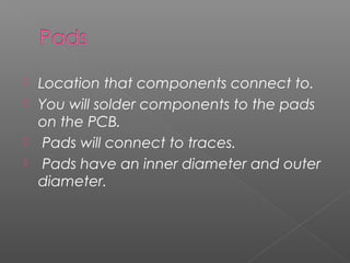
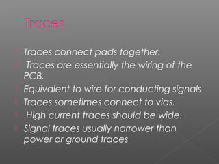
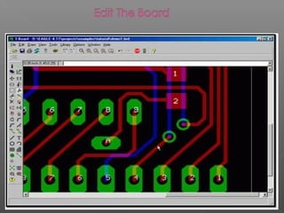
- The key components of a PCB including pads, traces, vias, and layers
- The PCB fabrication process including film generation, drilling, electroplating, imaging, etching, solder mask application, and silkscreening
- How components are attached to the board through surface mount or through-hole methods and the importance of carefully soldering to avoid shorts