Download to read offline
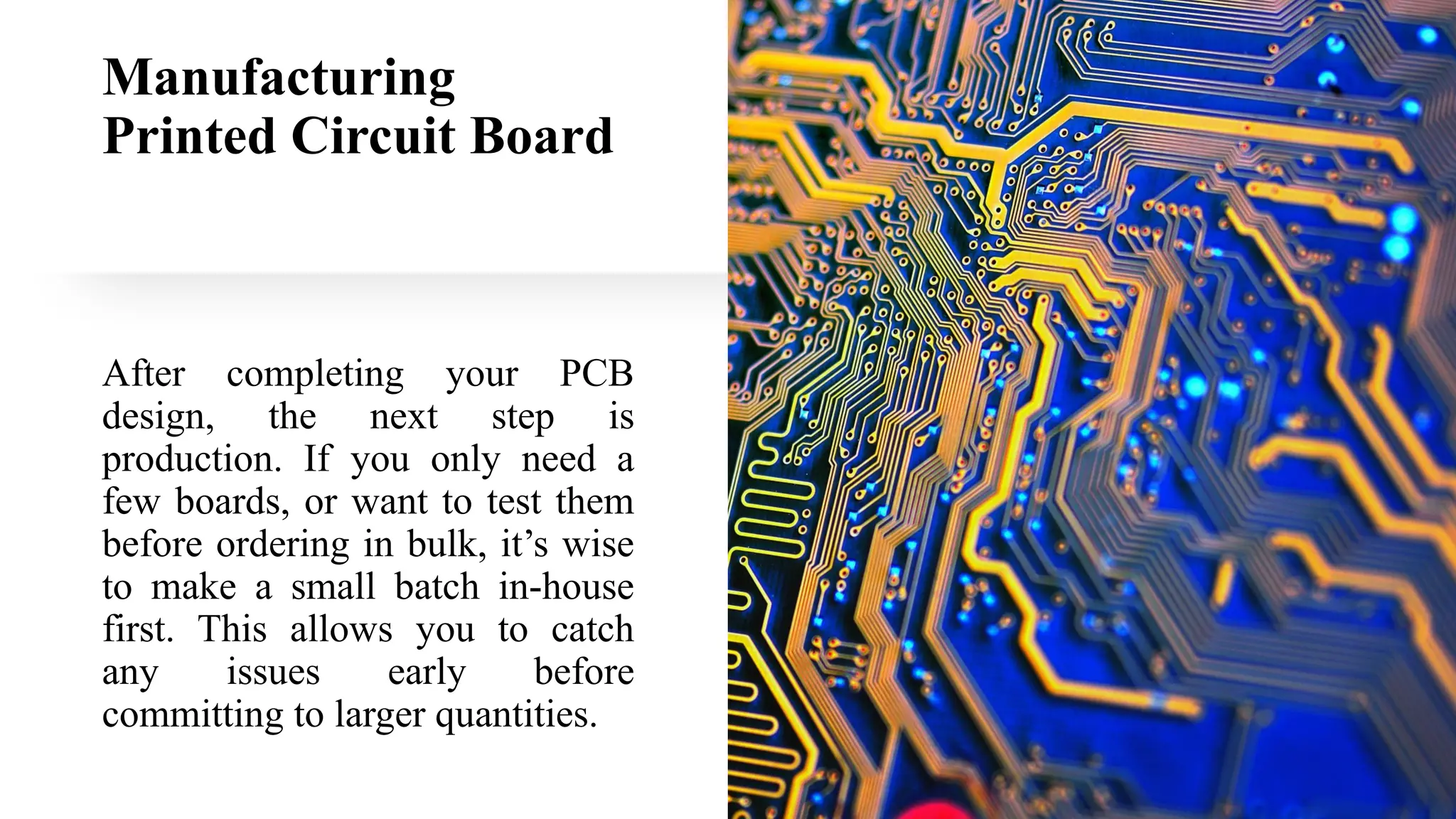


The document outlines the process of manufacturing printed circuit boards (PCBs) including design preparation, etching, milling, assembly, and testing. It discusses in-house production versus third-party manufacturing, detailing the necessary steps, tools, and costs involved. Additionally, it emphasizes the importance of testing and quality assurance to ensure the functionality and reliability of the final product.


![Defining Printed Circuit Board Assembly and Ways to do it [2022]](https://cdn.slidesharecdn.com/ss_thumbnails/definingprintedcircuitboardassemblyandwaystodoit2022-220131075935-thumbnail.jpg?width=640&height=640&fit=bounds)