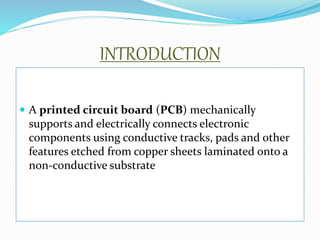
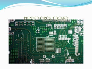
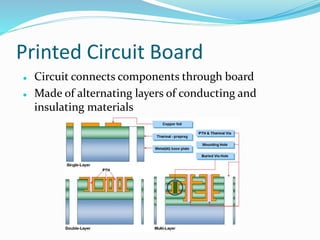
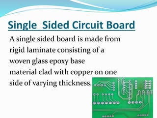
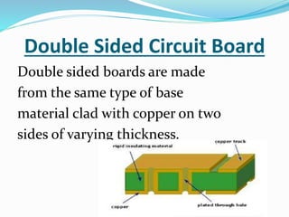
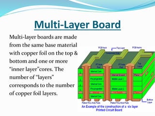
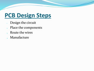
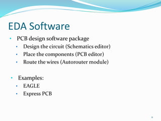
PCB DESIGN
BY- MAHESH KUMBAR
Future Robo System
INTRODUCTION
 A printed circuit board (PCB) mechanically
supports and electrically connects electronic
components using conductive tracks, pads and other
features etched from copper sheets laminated onto a
non-conductive substrate
PRINTED CIRCUIT BOARD
Printed Circuit Board
 Circuit connects components through board
 Made of alternating layers of conducting and
insulating materials
Why PCB?
• Features
• Surprisingly Affordable
• Highly reliable
• Compact
• Drawbacks
• Requires more layout than other board types
• Higher initial cost than wire wrap or point-to-point
construction
TYPES OF CIRCUIT BOARD
Single Sided Circuit Board
Double Sided Circuit Board
Multi-Layer Board
Single Sided Circuit Board
A single sided board is made from
rigid laminate consisting of a
woven glass epoxy base
material clad with copper on one
side of varying thickness.
Double Sided Circuit Board
Double sided boards are made
from the same type of base
material clad with copper on two
sides of varying thickness.
Multi-Layer Board
Multi-layer boards are made
from the same base material
with copper foil on the top &
bottom and one or more
“inner layer”cores. The
number of “layers”
corresponds to the number
of copper foil layers.
PCB Design Steps
1 Design the circuit
2 Place the components
3 Route the wires
4 Manufacture
EDA Software
• PCB design software package
• Design the circuit (Schematics editor)
• Place the components (PCB editor)
• Route the wires (Autorouter module)
• Examples:
• EAGLE
• Express PCB
11
Schematic Capture
 Pin in/outs
 Components
 Interconnections
 Easily Readable
 High-Level Block
Diagram
12
Placement of Components
• Place big components first- e.g. microcontroller
• Place components in separate functional groups
• Put a ground plane under all components
13
Signal Routing Component
Placement
 Surface mount
• Top and bottom planes
• Minimal routing area
 Through-hole mounted
• All components on same side
• Reduces routing area on all planes
14
Signal Routing
 Traces are wires connecting components
 Traces can be routed through multiple layers
15
Manufacturing
 Etching process
• Industry standard file format to describe circuits
• Generated by PCB design software
• Contains all necessary info to manufacture a circuit
board (Traces, Pads, Silkscreen, etc.) by UV Exposure
• Put in to ferric chloride chemical
16
Manufacturing
 Drill
• Describes the location and size of holes
• Zipped with Gerber files and sent to assembly
 PLACE THE COMPONENTS
 SOULDER THE COMPONENTS AS PER CIRCUIT DIAGRAM
WelcomePCB

WelcomePCB

  • 1.
    PCB DESIGN BY- MAHESHKUMBAR Future Robo System
  • 2.
    INTRODUCTION  A printedcircuit board (PCB) mechanically supports and electrically connects electronic components using conductive tracks, pads and other features etched from copper sheets laminated onto a non-conductive substrate
  • 3.
  • 4.
    Printed Circuit Board Circuit connects components through board  Made of alternating layers of conducting and insulating materials
  • 5.
    Why PCB? • Features •Surprisingly Affordable • Highly reliable • Compact • Drawbacks • Requires more layout than other board types • Higher initial cost than wire wrap or point-to-point construction
  • 6.
    TYPES OF CIRCUITBOARD Single Sided Circuit Board Double Sided Circuit Board Multi-Layer Board
  • 7.
    Single Sided CircuitBoard A single sided board is made from rigid laminate consisting of a woven glass epoxy base material clad with copper on one side of varying thickness.
  • 8.
    Double Sided CircuitBoard Double sided boards are made from the same type of base material clad with copper on two sides of varying thickness.
  • 9.
    Multi-Layer Board Multi-layer boardsare made from the same base material with copper foil on the top & bottom and one or more “inner layer”cores. The number of “layers” corresponds to the number of copper foil layers.
  • 10.
    PCB Design Steps 1Design the circuit 2 Place the components 3 Route the wires 4 Manufacture
  • 11.
    EDA Software • PCBdesign software package • Design the circuit (Schematics editor) • Place the components (PCB editor) • Route the wires (Autorouter module) • Examples: • EAGLE • Express PCB 11
  • 12.
    Schematic Capture  Pinin/outs  Components  Interconnections  Easily Readable  High-Level Block Diagram 12
  • 13.
    Placement of Components •Place big components first- e.g. microcontroller • Place components in separate functional groups • Put a ground plane under all components 13
  • 14.
    Signal Routing Component Placement Surface mount • Top and bottom planes • Minimal routing area  Through-hole mounted • All components on same side • Reduces routing area on all planes 14
  • 15.
    Signal Routing  Tracesare wires connecting components  Traces can be routed through multiple layers 15
  • 16.
    Manufacturing  Etching process •Industry standard file format to describe circuits • Generated by PCB design software • Contains all necessary info to manufacture a circuit board (Traces, Pads, Silkscreen, etc.) by UV Exposure • Put in to ferric chloride chemical 16
  • 17.
    Manufacturing  Drill • Describesthe location and size of holes • Zipped with Gerber files and sent to assembly  PLACE THE COMPONENTS  SOULDER THE COMPONENTS AS PER CIRCUIT DIAGRAM