SlideShare a Scribd company logo
1 of 8
Printed Circuit Board (PCB)
A printed circuit board (PCB) is a laminated sandwich structure of conductive and
insulating layers. PCBs have two complementary functions.
1. To affix electronic components in designated locations on the outer layers by means of
soldering.
2. To provide reliable electrical connections (and also reliable open circuits) between the
component's terminals in a controlled manner often referred to as PCB design.
PCBs mechanically support electronic components using conductive pads in the shape
designed to accept the component's terminals, and also electrically connect them using
traces, planes and other features etched from one or more sheet layers of
copper laminated onto and/or between sheet layers of a non-conductive substrate.
Through-hole technology
Surface-mount technology
Surface mount PCBs assembly occurs when
electrical components (surface-mount
devices) are machine picked and mounted
directly onto the surface of the PCB. During
this process, thousands of electrical
components are attached and connected to
their contact pads using reflow soldering.
Through-hole technology, also spelled “thru-hole”,
refers to the mounting scheme used for electronic
components that involves the use of leads on the
components that are inserted into holes drilled in
PCBs and soldered to pads on the opposite side
either by manual assembly (hand placement) or by
the use of automated insertion mount machines.
Types of PCB fabrication
Double-Sided PCBs Multilayer PCBs
Rigid PCBs
Flex PCBs
Rigid-Flex PCBs
Single sided PCBs
PCB FABRICATION PROCESS
1. Designing of electronics circuits & layout
2. Layout printing
3. Preparing substrate (A printed circuit board needs structure and shape. It
also needs a platform or canvass to hold all of its other components.)
4. Etching
5. Drilling
6. Solder mask application
7. Component assembly
8. PCB testing
DESIGNING OF CIRCUIT & LAYOUT
Softwares for PCB designing:- Proteus Professional/Eagle
PCB layout designing :-
1. Defining Trace Widths
PCB layouts use traces to connect components, but how wide should these traces be? The required trace width
for different nets depends on three possible factors:
• Manufacturability. Traces cannot be too thin, otherwise they can't be reliably manufactured.
• Current. The current carried in a trace will determine the minimum required width to prevent the trace
from overheating. When the current is higher, the trace will need to be wider.
For traces that don't need specific impedance or high current, a 10 mil trace width is fine for the vast majority of
low current analog and digital signals. Printed circuit board traces that carry more than 0.3 A may need to be
wider. To check this, you can use the IPC-2152 nomograph to determine your PCB trace width for a required
current capacity and temperature rise limit.
“1 mil = 1/1000 inch = 0.001 inch”
2. Make important nodes accessible.
3. Give space between components.
4. Place components with the same orientation.
5. Print the layout to see if components' sizes match.
6. Exchange wiring directions between layers.
7. Do not mount the electronic components within 1.27mm around the non-mounting holes, such as
tooling hole and standard holes.
8. Avoid placing holes under the components such as the horizontally mounted resistors, inductors,
(electrolytic capacitors, etc., so as to avoid short-circuiting the vias and component.
ETCHING
• ETCHING is an intaglio printmaking process in which lines or areas are incised using acid into a metal
plate in order to hold the ink. In etching, the plate can be made of iron, copper, or zinc.
• Chemical etching is usually done with ammonium per sulphate or ferric chloride.
• Process for using PCB etching machine:
1. Prepare Ferric Chloride Solution in the ratio of 1 KG Solid Ferric Chloride in 2 liters of water.
2. Put the solution in tank till the level touches 70% of the tank capacity. Make sure the heater and
temperature sensor tube is dipped in solution.
3. Set temperature to 50-55°C and after the solution is heated up to this temperature, dip the PCB hanged in
the hanger provided with the machine for 4-5 minutes.
4. Keep on inspecting the PCB after every 2 mins to avoid over etching.
DRILLING
PCB drilling, or printed circuit board drilling, is the process of creating holes, slots, and other cavities into an
electronic circuit board before soldering/mounting components onto it. It is typically done by using a PCB drill
bit (an automated machine) that is slightly smaller than the components placed on it.
Single-sided or double-sided PCB will be drilled directly after getting on the production line. Multi-layer
board will be drilled after pressuring layers. By classification of the function, different drilling holes can be
divided: through the hole, blind hole, Buried hole, etc.
SOLDER MASKING, COMPONENT
ASSEMBLY, PCB TESTING
A Solder mask is a protective coating over PCBs that prevents oxidation and electrical shorts. The solder
mask is coated over the entire board apart from the solder pads. The traditional green color coating that you see
on the PCBs is the solder mask. Uses Resin to coat the PCB to protect it from damage.
Soldering all components on right place leads to component assembly. And the resultant PCB is called as
Assembled PCB.
Final step in fabrication is – PCB Testing- which verifies the working of complete circuitry. Can be done by
manual , automated optical inspection , flying probe, x-ray inspection, etc methods.

More Related Content

What's hot

Surface mount Devices(SMD)
Surface mount Devices(SMD)Surface mount Devices(SMD)
Surface mount Devices(SMD)shyamaliamale
 
Introduction to PCB Designing
Introduction to PCB DesigningIntroduction to PCB Designing
Introduction to PCB DesigningSharan kumar
 
Surface mount technology(smt)
Surface mount technology(smt)Surface mount technology(smt)
Surface mount technology(smt)AshutoshKumar1262
 
Pcb manufacturing
Pcb manufacturingPcb manufacturing
Pcb manufacturingClement Ang
 
Printed Circuit Board Basics
Printed Circuit Board BasicsPrinted Circuit Board Basics
Printed Circuit Board BasicsSierra Assembly
 
training_presentation
training_presentationtraining_presentation
training_presentationAniket Pawar
 
PCB Fabrication Process by Sierra Assembly
PCB Fabrication Process by Sierra Assembly PCB Fabrication Process by Sierra Assembly
PCB Fabrication Process by Sierra Assembly Sierra Assembly
 
Printed circuit board
Printed circuit boardPrinted circuit board
Printed circuit boardSuhail Ahmed
 
Introduction to PCB Design
Introduction to PCB DesignIntroduction to PCB Design
Introduction to PCB DesignSharan kumar
 
Designing process of printed circuit boards
Designing process of printed circuit boardsDesigning process of printed circuit boards
Designing process of printed circuit boardselprocus
 
Design of Printed Circuit Boards
Design of Printed Circuit BoardsDesign of Printed Circuit Boards
Design of Printed Circuit BoardsChandana129742
 
Types of PCB Designing Layers
Types of PCB Designing LayersTypes of PCB Designing Layers
Types of PCB Designing LayersSharan kumar
 
Packaging of vlsi devices
Packaging of vlsi devicesPackaging of vlsi devices
Packaging of vlsi devicesAshu0711
 

What's hot (20)

CMOS
CMOS CMOS
CMOS
 
WelcomePCB
WelcomePCBWelcomePCB
WelcomePCB
 
Surface mount Devices(SMD)
Surface mount Devices(SMD)Surface mount Devices(SMD)
Surface mount Devices(SMD)
 
Pcb design powerpoint
Pcb design powerpointPcb design powerpoint
Pcb design powerpoint
 
Introduction to PCB Designing
Introduction to PCB DesigningIntroduction to PCB Designing
Introduction to PCB Designing
 
Surface mount technology(smt)
Surface mount technology(smt)Surface mount technology(smt)
Surface mount technology(smt)
 
INTRODUCTION TO PCB
INTRODUCTION TO PCBINTRODUCTION TO PCB
INTRODUCTION TO PCB
 
Pcb manufacturing
Pcb manufacturingPcb manufacturing
Pcb manufacturing
 
Printed Circuit Board Basics
Printed Circuit Board BasicsPrinted Circuit Board Basics
Printed Circuit Board Basics
 
training_presentation
training_presentationtraining_presentation
training_presentation
 
PCB Fabrication Process by Sierra Assembly
PCB Fabrication Process by Sierra Assembly PCB Fabrication Process by Sierra Assembly
PCB Fabrication Process by Sierra Assembly
 
Multi chip module
Multi chip moduleMulti chip module
Multi chip module
 
Printed circuit board
Printed circuit boardPrinted circuit board
Printed circuit board
 
Smt basics
Smt basicsSmt basics
Smt basics
 
Introduction to PCB Design
Introduction to PCB DesignIntroduction to PCB Design
Introduction to PCB Design
 
PCB Designing
PCB Designing PCB Designing
PCB Designing
 
Designing process of printed circuit boards
Designing process of printed circuit boardsDesigning process of printed circuit boards
Designing process of printed circuit boards
 
Design of Printed Circuit Boards
Design of Printed Circuit BoardsDesign of Printed Circuit Boards
Design of Printed Circuit Boards
 
Types of PCB Designing Layers
Types of PCB Designing LayersTypes of PCB Designing Layers
Types of PCB Designing Layers
 
Packaging of vlsi devices
Packaging of vlsi devicesPackaging of vlsi devices
Packaging of vlsi devices
 

Similar to PCB fabrication.pptx

GabunaMary-Joy-D.Procedures-in-making-PCB.pptx
GabunaMary-Joy-D.Procedures-in-making-PCB.pptxGabunaMary-Joy-D.Procedures-in-making-PCB.pptx
GabunaMary-Joy-D.Procedures-in-making-PCB.pptxChristopherGalivo
 
PCB Fabrication, China PCB Circuit Board Manufacturing from China
PCB Fabrication, China PCB Circuit Board Manufacturing from ChinaPCB Fabrication, China PCB Circuit Board Manufacturing from China
PCB Fabrication, China PCB Circuit Board Manufacturing from ChinaLeah-Hitech PCB
 
Learning outcome 2 prepare make pcb modules
Learning outcome 2 prepare make pcb modulesLearning outcome 2 prepare make pcb modules
Learning outcome 2 prepare make pcb modulesAr Kyu Dee
 
Importance of PCB assembly in Various Industries | Suntronic Inc |
Importance of PCB assembly in Various Industries | Suntronic Inc |Importance of PCB assembly in Various Industries | Suntronic Inc |
Importance of PCB assembly in Various Industries | Suntronic Inc |SuntronicInc
 
PCB Terminologies in PCB designing
PCB Terminologies in PCB designingPCB Terminologies in PCB designing
PCB Terminologies in PCB designingMSHOAIBASLAM1
 
presentation1-131031235854-phpapp02.pptx
presentation1-131031235854-phpapp02.pptxpresentation1-131031235854-phpapp02.pptx
presentation1-131031235854-phpapp02.pptxSirachartChuto
 
Chapter12 manufacturing-processes
Chapter12 manufacturing-processesChapter12 manufacturing-processes
Chapter12 manufacturing-processesVin Voro
 
Pcb design using_eagle
Pcb design using_eaglePcb design using_eagle
Pcb design using_eagleABDUL MUNAFF
 
Pcbdesign 140510145153-phpapp01
Pcbdesign 140510145153-phpapp01Pcbdesign 140510145153-phpapp01
Pcbdesign 140510145153-phpapp01ssantosh1234
 
Surface mount technology (smt) and smd packages
Surface mount technology (smt) and smd packagesSurface mount technology (smt) and smd packages
Surface mount technology (smt) and smd packageskaren zou
 
Through hole technology for pcb board from wonderful pcb
Through hole technology for pcb board from wonderful pcbThrough hole technology for pcb board from wonderful pcb
Through hole technology for pcb board from wonderful pcbWonderful PCB Lcd
 

Similar to PCB fabrication.pptx (20)

GabunaMary-Joy-D.Procedures-in-making-PCB.pptx
GabunaMary-Joy-D.Procedures-in-making-PCB.pptxGabunaMary-Joy-D.Procedures-in-making-PCB.pptx
GabunaMary-Joy-D.Procedures-in-making-PCB.pptx
 
PCB Fabrication, China PCB Circuit Board Manufacturing from China
PCB Fabrication, China PCB Circuit Board Manufacturing from ChinaPCB Fabrication, China PCB Circuit Board Manufacturing from China
PCB Fabrication, China PCB Circuit Board Manufacturing from China
 
PCB Assembly Manufacturer Hitech circuits
PCB Assembly Manufacturer Hitech circuitsPCB Assembly Manufacturer Hitech circuits
PCB Assembly Manufacturer Hitech circuits
 
Learning outcome 2 prepare make pcb modules
Learning outcome 2 prepare make pcb modulesLearning outcome 2 prepare make pcb modules
Learning outcome 2 prepare make pcb modules
 
Importance of PCB assembly in Various Industries | Suntronic Inc |
Importance of PCB assembly in Various Industries | Suntronic Inc |Importance of PCB assembly in Various Industries | Suntronic Inc |
Importance of PCB assembly in Various Industries | Suntronic Inc |
 
PCB Terminologies in PCB designing
PCB Terminologies in PCB designingPCB Terminologies in PCB designing
PCB Terminologies in PCB designing
 
presentation1-131031235854-phpapp02.pptx
presentation1-131031235854-phpapp02.pptxpresentation1-131031235854-phpapp02.pptx
presentation1-131031235854-phpapp02.pptx
 
PCB
PCBPCB
PCB
 
Chapter12 manufacturing-processes
Chapter12 manufacturing-processesChapter12 manufacturing-processes
Chapter12 manufacturing-processes
 
PCB
PCBPCB
PCB
 
Pcb design using_eagle
Pcb design using_eaglePcb design using_eagle
Pcb design using_eagle
 
Pcbdesign 140510145153-phpapp01
Pcbdesign 140510145153-phpapp01Pcbdesign 140510145153-phpapp01
Pcbdesign 140510145153-phpapp01
 
PCB desine final.pdf
PCB desine final.pdfPCB desine final.pdf
PCB desine final.pdf
 
ORCAD pcb design
ORCAD pcb designORCAD pcb design
ORCAD pcb design
 
ACHAL NEET PPT OF PCB-1.pptx
ACHAL NEET PPT OF PCB-1.pptxACHAL NEET PPT OF PCB-1.pptx
ACHAL NEET PPT OF PCB-1.pptx
 
Assembly
AssemblyAssembly
Assembly
 
PCB
PCBPCB
PCB
 
Surface mount technology (smt) and smd packages
Surface mount technology (smt) and smd packagesSurface mount technology (smt) and smd packages
Surface mount technology (smt) and smd packages
 
Through hole technology for pcb board from wonderful pcb
Through hole technology for pcb board from wonderful pcbThrough hole technology for pcb board from wonderful pcb
Through hole technology for pcb board from wonderful pcb
 
Jsk urja pcb ppt
Jsk urja pcb pptJsk urja pcb ppt
Jsk urja pcb ppt
 

Recently uploaded

Call Girls in Nagpur Bhavna Call 7001035870 Meet With Nagpur Escorts
Call Girls in Nagpur Bhavna Call 7001035870 Meet With Nagpur EscortsCall Girls in Nagpur Bhavna Call 7001035870 Meet With Nagpur Escorts
Call Girls in Nagpur Bhavna Call 7001035870 Meet With Nagpur Escortsranjana rawat
 
如何办理(UCLA毕业证书)加州大学洛杉矶分校毕业证成绩单留信学历认证原版一比一
如何办理(UCLA毕业证书)加州大学洛杉矶分校毕业证成绩单留信学历认证原版一比一如何办理(UCLA毕业证书)加州大学洛杉矶分校毕业证成绩单留信学历认证原版一比一
如何办理(UCLA毕业证书)加州大学洛杉矶分校毕业证成绩单留信学历认证原版一比一ga6c6bdl
 
如何办理(Adelaide毕业证)阿德莱德大学毕业证成绩单Adelaide学历认证真实可查
如何办理(Adelaide毕业证)阿德莱德大学毕业证成绩单Adelaide学历认证真实可查如何办理(Adelaide毕业证)阿德莱德大学毕业证成绩单Adelaide学历认证真实可查
如何办理(Adelaide毕业证)阿德莱德大学毕业证成绩单Adelaide学历认证真实可查awo24iot
 
(MEGHA) Hinjewadi Call Girls Just Call 7001035870 [ Cash on Delivery ] Pune E...
(MEGHA) Hinjewadi Call Girls Just Call 7001035870 [ Cash on Delivery ] Pune E...(MEGHA) Hinjewadi Call Girls Just Call 7001035870 [ Cash on Delivery ] Pune E...
(MEGHA) Hinjewadi Call Girls Just Call 7001035870 [ Cash on Delivery ] Pune E...ranjana rawat
 
(SANA) Call Girls Landewadi ( 7001035870 ) HI-Fi Pune Escorts Service
(SANA) Call Girls Landewadi ( 7001035870 ) HI-Fi Pune Escorts Service(SANA) Call Girls Landewadi ( 7001035870 ) HI-Fi Pune Escorts Service
(SANA) Call Girls Landewadi ( 7001035870 ) HI-Fi Pune Escorts Serviceranjana rawat
 
如何办理(NUS毕业证书)新加坡国立大学毕业证成绩单留信学历认证原版一比一
如何办理(NUS毕业证书)新加坡国立大学毕业证成绩单留信学历认证原版一比一如何办理(NUS毕业证书)新加坡国立大学毕业证成绩单留信学历认证原版一比一
如何办理(NUS毕业证书)新加坡国立大学毕业证成绩单留信学历认证原版一比一ga6c6bdl
 
Russian Call Girls Kolkata Chhaya 🤌 8250192130 🚀 Vip Call Girls Kolkata
Russian Call Girls Kolkata Chhaya 🤌  8250192130 🚀 Vip Call Girls KolkataRussian Call Girls Kolkata Chhaya 🤌  8250192130 🚀 Vip Call Girls Kolkata
Russian Call Girls Kolkata Chhaya 🤌 8250192130 🚀 Vip Call Girls Kolkataanamikaraghav4
 
(ZARA) Call Girls Jejuri ( 7001035870 ) HI-Fi Pune Escorts Service
(ZARA) Call Girls Jejuri ( 7001035870 ) HI-Fi Pune Escorts Service(ZARA) Call Girls Jejuri ( 7001035870 ) HI-Fi Pune Escorts Service
(ZARA) Call Girls Jejuri ( 7001035870 ) HI-Fi Pune Escorts Serviceranjana rawat
 
Russian Call Girls In South Delhi Delhi 9711199012 💋✔💕😘 Independent Escorts D...
Russian Call Girls In South Delhi Delhi 9711199012 💋✔💕😘 Independent Escorts D...Russian Call Girls In South Delhi Delhi 9711199012 💋✔💕😘 Independent Escorts D...
Russian Call Girls In South Delhi Delhi 9711199012 💋✔💕😘 Independent Escorts D...nagunakhan
 
VIP Call Girls Kavuri Hills ( Hyderabad ) Phone 8250192130 | ₹5k To 25k With ...
VIP Call Girls Kavuri Hills ( Hyderabad ) Phone 8250192130 | ₹5k To 25k With ...VIP Call Girls Kavuri Hills ( Hyderabad ) Phone 8250192130 | ₹5k To 25k With ...
VIP Call Girls Kavuri Hills ( Hyderabad ) Phone 8250192130 | ₹5k To 25k With ...Suhani Kapoor
 
Call Girls Delhi {Rs-10000 Laxmi Nagar] 9711199012 Whats Up Number
Call Girls Delhi {Rs-10000 Laxmi Nagar] 9711199012 Whats Up NumberCall Girls Delhi {Rs-10000 Laxmi Nagar] 9711199012 Whats Up Number
Call Girls Delhi {Rs-10000 Laxmi Nagar] 9711199012 Whats Up NumberMs Riya
 
Lucknow 💋 Call Girls Adil Nagar | ₹,9500 Pay Cash 8923113531 Free Home Delive...
Lucknow 💋 Call Girls Adil Nagar | ₹,9500 Pay Cash 8923113531 Free Home Delive...Lucknow 💋 Call Girls Adil Nagar | ₹,9500 Pay Cash 8923113531 Free Home Delive...
Lucknow 💋 Call Girls Adil Nagar | ₹,9500 Pay Cash 8923113531 Free Home Delive...anilsa9823
 
Presentation.pptxjnfoigneoifnvoeifnvklfnvf
Presentation.pptxjnfoigneoifnvoeifnvklfnvfPresentation.pptxjnfoigneoifnvoeifnvklfnvf
Presentation.pptxjnfoigneoifnvoeifnvklfnvfchapmanellie27
 
9004554577, Get Adorable Call Girls service. Book call girls & escort service...
9004554577, Get Adorable Call Girls service. Book call girls & escort service...9004554577, Get Adorable Call Girls service. Book call girls & escort service...
9004554577, Get Adorable Call Girls service. Book call girls & escort service...Pooja Nehwal
 
VVIP Pune Call Girls Balaji Nagar (7001035870) Pune Escorts Nearby with Compl...
VVIP Pune Call Girls Balaji Nagar (7001035870) Pune Escorts Nearby with Compl...VVIP Pune Call Girls Balaji Nagar (7001035870) Pune Escorts Nearby with Compl...
VVIP Pune Call Girls Balaji Nagar (7001035870) Pune Escorts Nearby with Compl...Call Girls in Nagpur High Profile
 
Call Girls in Thane 9892124323, Vashi cAll girls Serivces Juhu Escorts, powai...
Call Girls in Thane 9892124323, Vashi cAll girls Serivces Juhu Escorts, powai...Call Girls in Thane 9892124323, Vashi cAll girls Serivces Juhu Escorts, powai...
Call Girls in Thane 9892124323, Vashi cAll girls Serivces Juhu Escorts, powai...Pooja Nehwal
 
Pallawi 9167673311 Call Girls in Thane , Independent Escort Service Thane
Pallawi 9167673311  Call Girls in Thane , Independent Escort Service ThanePallawi 9167673311  Call Girls in Thane , Independent Escort Service Thane
Pallawi 9167673311 Call Girls in Thane , Independent Escort Service ThanePooja Nehwal
 
Thane Escorts, (Pooja 09892124323), Thane Call Girls
Thane Escorts, (Pooja 09892124323), Thane Call GirlsThane Escorts, (Pooja 09892124323), Thane Call Girls
Thane Escorts, (Pooja 09892124323), Thane Call GirlsPooja Nehwal
 

Recently uploaded (20)

Call Girls in Nagpur Bhavna Call 7001035870 Meet With Nagpur Escorts
Call Girls in Nagpur Bhavna Call 7001035870 Meet With Nagpur EscortsCall Girls in Nagpur Bhavna Call 7001035870 Meet With Nagpur Escorts
Call Girls in Nagpur Bhavna Call 7001035870 Meet With Nagpur Escorts
 
如何办理(UCLA毕业证书)加州大学洛杉矶分校毕业证成绩单留信学历认证原版一比一
如何办理(UCLA毕业证书)加州大学洛杉矶分校毕业证成绩单留信学历认证原版一比一如何办理(UCLA毕业证书)加州大学洛杉矶分校毕业证成绩单留信学历认证原版一比一
如何办理(UCLA毕业证书)加州大学洛杉矶分校毕业证成绩单留信学历认证原版一比一
 
如何办理(Adelaide毕业证)阿德莱德大学毕业证成绩单Adelaide学历认证真实可查
如何办理(Adelaide毕业证)阿德莱德大学毕业证成绩单Adelaide学历认证真实可查如何办理(Adelaide毕业证)阿德莱德大学毕业证成绩单Adelaide学历认证真实可查
如何办理(Adelaide毕业证)阿德莱德大学毕业证成绩单Adelaide学历认证真实可查
 
(MEGHA) Hinjewadi Call Girls Just Call 7001035870 [ Cash on Delivery ] Pune E...
(MEGHA) Hinjewadi Call Girls Just Call 7001035870 [ Cash on Delivery ] Pune E...(MEGHA) Hinjewadi Call Girls Just Call 7001035870 [ Cash on Delivery ] Pune E...
(MEGHA) Hinjewadi Call Girls Just Call 7001035870 [ Cash on Delivery ] Pune E...
 
(SANA) Call Girls Landewadi ( 7001035870 ) HI-Fi Pune Escorts Service
(SANA) Call Girls Landewadi ( 7001035870 ) HI-Fi Pune Escorts Service(SANA) Call Girls Landewadi ( 7001035870 ) HI-Fi Pune Escorts Service
(SANA) Call Girls Landewadi ( 7001035870 ) HI-Fi Pune Escorts Service
 
如何办理(NUS毕业证书)新加坡国立大学毕业证成绩单留信学历认证原版一比一
如何办理(NUS毕业证书)新加坡国立大学毕业证成绩单留信学历认证原版一比一如何办理(NUS毕业证书)新加坡国立大学毕业证成绩单留信学历认证原版一比一
如何办理(NUS毕业证书)新加坡国立大学毕业证成绩单留信学历认证原版一比一
 
Russian Call Girls Kolkata Chhaya 🤌 8250192130 🚀 Vip Call Girls Kolkata
Russian Call Girls Kolkata Chhaya 🤌  8250192130 🚀 Vip Call Girls KolkataRussian Call Girls Kolkata Chhaya 🤌  8250192130 🚀 Vip Call Girls Kolkata
Russian Call Girls Kolkata Chhaya 🤌 8250192130 🚀 Vip Call Girls Kolkata
 
(ZARA) Call Girls Jejuri ( 7001035870 ) HI-Fi Pune Escorts Service
(ZARA) Call Girls Jejuri ( 7001035870 ) HI-Fi Pune Escorts Service(ZARA) Call Girls Jejuri ( 7001035870 ) HI-Fi Pune Escorts Service
(ZARA) Call Girls Jejuri ( 7001035870 ) HI-Fi Pune Escorts Service
 
Russian Call Girls In South Delhi Delhi 9711199012 💋✔💕😘 Independent Escorts D...
Russian Call Girls In South Delhi Delhi 9711199012 💋✔💕😘 Independent Escorts D...Russian Call Girls In South Delhi Delhi 9711199012 💋✔💕😘 Independent Escorts D...
Russian Call Girls In South Delhi Delhi 9711199012 💋✔💕😘 Independent Escorts D...
 
VIP Call Girls Kavuri Hills ( Hyderabad ) Phone 8250192130 | ₹5k To 25k With ...
VIP Call Girls Kavuri Hills ( Hyderabad ) Phone 8250192130 | ₹5k To 25k With ...VIP Call Girls Kavuri Hills ( Hyderabad ) Phone 8250192130 | ₹5k To 25k With ...
VIP Call Girls Kavuri Hills ( Hyderabad ) Phone 8250192130 | ₹5k To 25k With ...
 
Call Girls Delhi {Rs-10000 Laxmi Nagar] 9711199012 Whats Up Number
Call Girls Delhi {Rs-10000 Laxmi Nagar] 9711199012 Whats Up NumberCall Girls Delhi {Rs-10000 Laxmi Nagar] 9711199012 Whats Up Number
Call Girls Delhi {Rs-10000 Laxmi Nagar] 9711199012 Whats Up Number
 
Lucknow 💋 Call Girls Adil Nagar | ₹,9500 Pay Cash 8923113531 Free Home Delive...
Lucknow 💋 Call Girls Adil Nagar | ₹,9500 Pay Cash 8923113531 Free Home Delive...Lucknow 💋 Call Girls Adil Nagar | ₹,9500 Pay Cash 8923113531 Free Home Delive...
Lucknow 💋 Call Girls Adil Nagar | ₹,9500 Pay Cash 8923113531 Free Home Delive...
 
Presentation.pptxjnfoigneoifnvoeifnvklfnvf
Presentation.pptxjnfoigneoifnvoeifnvklfnvfPresentation.pptxjnfoigneoifnvoeifnvklfnvf
Presentation.pptxjnfoigneoifnvoeifnvklfnvf
 
9004554577, Get Adorable Call Girls service. Book call girls & escort service...
9004554577, Get Adorable Call Girls service. Book call girls & escort service...9004554577, Get Adorable Call Girls service. Book call girls & escort service...
9004554577, Get Adorable Call Girls service. Book call girls & escort service...
 
VVIP Pune Call Girls Balaji Nagar (7001035870) Pune Escorts Nearby with Compl...
VVIP Pune Call Girls Balaji Nagar (7001035870) Pune Escorts Nearby with Compl...VVIP Pune Call Girls Balaji Nagar (7001035870) Pune Escorts Nearby with Compl...
VVIP Pune Call Girls Balaji Nagar (7001035870) Pune Escorts Nearby with Compl...
 
Call Girls in Thane 9892124323, Vashi cAll girls Serivces Juhu Escorts, powai...
Call Girls in Thane 9892124323, Vashi cAll girls Serivces Juhu Escorts, powai...Call Girls in Thane 9892124323, Vashi cAll girls Serivces Juhu Escorts, powai...
Call Girls in Thane 9892124323, Vashi cAll girls Serivces Juhu Escorts, powai...
 
Pallawi 9167673311 Call Girls in Thane , Independent Escort Service Thane
Pallawi 9167673311  Call Girls in Thane , Independent Escort Service ThanePallawi 9167673311  Call Girls in Thane , Independent Escort Service Thane
Pallawi 9167673311 Call Girls in Thane , Independent Escort Service Thane
 
Low rate Call girls in Delhi Justdial | 9953330565
Low rate Call girls in Delhi Justdial | 9953330565Low rate Call girls in Delhi Justdial | 9953330565
Low rate Call girls in Delhi Justdial | 9953330565
 
9953330565 Low Rate Call Girls In Jahangirpuri Delhi NCR
9953330565 Low Rate Call Girls In Jahangirpuri  Delhi NCR9953330565 Low Rate Call Girls In Jahangirpuri  Delhi NCR
9953330565 Low Rate Call Girls In Jahangirpuri Delhi NCR
 
Thane Escorts, (Pooja 09892124323), Thane Call Girls
Thane Escorts, (Pooja 09892124323), Thane Call GirlsThane Escorts, (Pooja 09892124323), Thane Call Girls
Thane Escorts, (Pooja 09892124323), Thane Call Girls
 

PCB fabrication.pptx

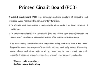
  • 1. Printed Circuit Board (PCB) A printed circuit board (PCB) is a laminated sandwich structure of conductive and insulating layers. PCBs have two complementary functions. 1. To affix electronic components in designated locations on the outer layers by means of soldering. 2. To provide reliable electrical connections (and also reliable open circuits) between the component's terminals in a controlled manner often referred to as PCB design. PCBs mechanically support electronic components using conductive pads in the shape designed to accept the component's terminals, and also electrically connect them using traces, planes and other features etched from one or more sheet layers of copper laminated onto and/or between sheet layers of a non-conductive substrate. Through-hole technology Surface-mount technology
  • 2. Surface mount PCBs assembly occurs when electrical components (surface-mount devices) are machine picked and mounted directly onto the surface of the PCB. During this process, thousands of electrical components are attached and connected to their contact pads using reflow soldering. Through-hole technology, also spelled “thru-hole”, refers to the mounting scheme used for electronic components that involves the use of leads on the components that are inserted into holes drilled in PCBs and soldered to pads on the opposite side either by manual assembly (hand placement) or by the use of automated insertion mount machines.
  • 3. Types of PCB fabrication Double-Sided PCBs Multilayer PCBs Rigid PCBs Flex PCBs Rigid-Flex PCBs Single sided PCBs
  • 4. PCB FABRICATION PROCESS 1. Designing of electronics circuits & layout 2. Layout printing 3. Preparing substrate (A printed circuit board needs structure and shape. It also needs a platform or canvass to hold all of its other components.) 4. Etching 5. Drilling 6. Solder mask application 7. Component assembly 8. PCB testing
  • 5. DESIGNING OF CIRCUIT & LAYOUT Softwares for PCB designing:- Proteus Professional/Eagle PCB layout designing :- 1. Defining Trace Widths PCB layouts use traces to connect components, but how wide should these traces be? The required trace width for different nets depends on three possible factors: • Manufacturability. Traces cannot be too thin, otherwise they can't be reliably manufactured. • Current. The current carried in a trace will determine the minimum required width to prevent the trace from overheating. When the current is higher, the trace will need to be wider. For traces that don't need specific impedance or high current, a 10 mil trace width is fine for the vast majority of low current analog and digital signals. Printed circuit board traces that carry more than 0.3 A may need to be wider. To check this, you can use the IPC-2152 nomograph to determine your PCB trace width for a required current capacity and temperature rise limit. “1 mil = 1/1000 inch = 0.001 inch” 2. Make important nodes accessible. 3. Give space between components. 4. Place components with the same orientation. 5. Print the layout to see if components' sizes match. 6. Exchange wiring directions between layers. 7. Do not mount the electronic components within 1.27mm around the non-mounting holes, such as tooling hole and standard holes. 8. Avoid placing holes under the components such as the horizontally mounted resistors, inductors, (electrolytic capacitors, etc., so as to avoid short-circuiting the vias and component.
  • 6. ETCHING • ETCHING is an intaglio printmaking process in which lines or areas are incised using acid into a metal plate in order to hold the ink. In etching, the plate can be made of iron, copper, or zinc. • Chemical etching is usually done with ammonium per sulphate or ferric chloride. • Process for using PCB etching machine: 1. Prepare Ferric Chloride Solution in the ratio of 1 KG Solid Ferric Chloride in 2 liters of water. 2. Put the solution in tank till the level touches 70% of the tank capacity. Make sure the heater and temperature sensor tube is dipped in solution. 3. Set temperature to 50-55°C and after the solution is heated up to this temperature, dip the PCB hanged in the hanger provided with the machine for 4-5 minutes. 4. Keep on inspecting the PCB after every 2 mins to avoid over etching.
  • 7. DRILLING PCB drilling, or printed circuit board drilling, is the process of creating holes, slots, and other cavities into an electronic circuit board before soldering/mounting components onto it. It is typically done by using a PCB drill bit (an automated machine) that is slightly smaller than the components placed on it. Single-sided or double-sided PCB will be drilled directly after getting on the production line. Multi-layer board will be drilled after pressuring layers. By classification of the function, different drilling holes can be divided: through the hole, blind hole, Buried hole, etc.
  • 8. SOLDER MASKING, COMPONENT ASSEMBLY, PCB TESTING A Solder mask is a protective coating over PCBs that prevents oxidation and electrical shorts. The solder mask is coated over the entire board apart from the solder pads. The traditional green color coating that you see on the PCBs is the solder mask. Uses Resin to coat the PCB to protect it from damage. Soldering all components on right place leads to component assembly. And the resultant PCB is called as Assembled PCB. Final step in fabrication is – PCB Testing- which verifies the working of complete circuitry. Can be done by manual , automated optical inspection , flying probe, x-ray inspection, etc methods.