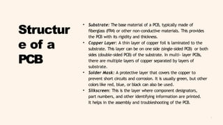
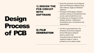
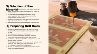
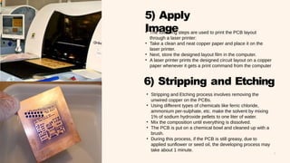
1
Printed
Circuit Board
Manufacturing
Presented by:
M. Pratusha-21261A0439
Meghna Goud-21261A0440
Ruhika Manomay-21261A0449
V Varsha-21261A0459
Under the guidance of
Dr. C.S.SRINIVAS
2
What Is PCB?
• PCB stands for Printed Circuit Board.
• It is a flat board used in electronics to mechanically support and electrically
connect electronic components using conductive pathways, tracks, or signal
traces etched from copper sheets laminated onto a non-conductive
substrate.
• The components on a PCB can include resistors, capacitors, diodes, transistors,
and integrated circuits, among several others.
• The circuits are designed on the boards with copper tracks instead of wires for
the conduction of electricity between the electronic components.
3
WhyPCB?
• Before the PCB was invented, the components
were connected in a point-to-point manner
i.e. pins of the components needed to be
connected to each other through soldering or
sockets to form a circuit path.
• However, this connection method was too
complicated and cumbersome causing a lot of
wires to get tangled.
• In order to find a new and more efficient way
to connect circuits, Charles Dukas drew circuit
patterns on insulating substrate materials and
built wiring conductors through electroplating,
known as the circuit pattern.
• The first PCB board was born in 1936, when
Austrian engineer Paul Eisler demonstrated a
radio with a PCB at a technical seminar in the
UK.
4
Types
of PCBs
Single-Sided PCBs
These have a single layer of copper on
one side of the substrate. They are
simple and inexpensive but limited in
complexity
Double-Sided PCBs
These have copper layers on both sides of
the substrate, allowing for more complex
circuits.
Multi-Layer PCBs
These consist of several layers of copper
separated by insulating layers. They are
used in more complex and compact devices,
like computer motherboards and advanced
communications equipment.
5
Structur
e of a
PCB
• Substrate: The base material of a PCB, typically made of
fiberglass (FR4) or other non-conductive materials. This provides
the PCB with its rigidity and thickness.
• Copper Layer: A thin layer of copper foil is laminated to the
substrate. This layer can be on one side (single-sided PCB) or both
sides (double-sided PCB) of the substrate. In multi- layer PCBs,
there are multiple layers of copper separated by layers of
substrate.
• Solder Mask: A protective layer that covers the copper to
prevent short circuits and corrosion. It is usually green, but other
colors like red, blue, or black can also be used.
• Silkscreen: This is the layer where component designators,
part numbers, and other identifying information are printed.
It helps in the assembly and troubleshooting of the PCB.
6
• Draw the schematic circuit diagram
with the PCB layout software.Using
CAD software, Eagle and Multisim
software.
• This type of PCB design software
contains a library of components that
can be used to build the circuit.
• It allows you to change the circuit
design's position, modification
according to your convenience and
requirement.
• The film is generated from the
finalized circuit board diagram
of the PCB layout software
which is send to the
manufacturing unit where the
negative image or mask is
printed out on a plastic sheet.
Design
Process
of PCB
2) FILM
GENERATION
1) DESIGN THE
PCB CIRCUIT
WITH
SOFTWARE
7
3) Selection of Raw
Material
• The bulk of the printed circuit board is made with an unbreakable
glass or fiberglass having copper foil bonded onto one or both the
sides of the board.
• The PCBs made from unbreakable paper phenolic with a
bonded copper foil. These are less expensive and are often
used in household electrical devices.
• Mostly 0.059 industry standard thick, copper clad laminate, either
single or double sided board is required.
• Panels may be sheared to contain many boards of different sizes.
• Machines and carbide drills are used to put holes on the printed
circuit board There are two types of machines available to drill
the PCBs.
• They include hand machines and CNC machines.
• The hand machines require human intervention or effort to
drill the holes. CNC machines are computer-based machines.
• It work-based on the machine timetables or programs that run both
automatic as well as manually.
• The drilled pattern is stored in the computer like drill bit sizes, number
of holes per panel, drilled stack, drilled time per load, etc.
• The PCB boards are placed into the CNC machine.
• The holes are drilled according to the determined pattern to place
printed circuit board components.
4) Preparing Drill Holes
8
5) Apply
Image
6) Stripping and Etching
• The following steps are used to print the PCB layout
through a laser printer:
• Take a clean and neat copper paper and place it on the
laser printer.
• Next, store the designed layout film in the computer.
• A laser printer prints the designed circuit layout on a copper
paper whenever it gets a print command from the computer
• Stripping and Etching process involves removing the
unwired copper on the PCBs.
• Using different types of chemicals like ferric chloride,
ammonium per-sulphate, etc. make the solvent by mixing
1% of sodium hydroxide pellets to one liter of water.
• Mix the composition until everything is dissolved.
• The PCB is put on a chemical bowl and cleaned up with a
brush.
• During this process, if the PCB is still greasy, due to
applied sunflower or seed oil, the developing process may
take about 1 minute.
9
7) Testing
• After finishing the manufacturing process of
the PCB, the board undergoes a testing
process to check whether the PCB is working
properly.
• While the power is off, visual inspection,
automated optical inspection. JEDEC
guidelines for PCB component placement,
soldering, and inspection are commonly used
to maintain quality control in this stage of
PCB manufacturing
• While the power is on, in-circuit test, where
physical measurements (for example,
voltage) can be done.
• While the power is on, functional test, just
checking if the PCB does what it had been
designed to do.
10
CONCLUSION
• Printed Circuit Boards (PCBs) play a crucial role in various applications across
different industries. Here are some real-world applications where PCBs are
essential:
• Automotive: High-current PCBs are used in automotive systems for
controlling engine functions, safety features, infotainment systems, and more.
• Medical: Medical devices rely on PCBs for precision and reliability. Examples
include X-ray machines, CT/CAT scanners, ultrasounds, blood glucose
monitors, heart rate monitors, and pacemakers.
• Telecommunications: PCBs are integral to communication infrastructure,
including cell towers, routers, and network equipment.
• Robotics: PCBs power robotic systems, controlling movement, sensors, and
communication.
• Industrial Applications: PCBs are used in industrial automation, control
systems, motor drives, and power electronics.
• If you’re interested in designing PCBs, consider tools like Altium
Designer (popular among professionals), KiCad (free and open-
source), EasyEDA (browser-based), and Upverter (great for students and
educators) . These tools offer various features to streamline your design
process.
11
THANK YOU

Printed Circuit Board.pptx

  • 1.
    1 Printed Circuit Board Manufacturing Presented by: M.Pratusha-21261A0439 Meghna Goud-21261A0440 Ruhika Manomay-21261A0449 V Varsha-21261A0459 Under the guidance of Dr. C.S.SRINIVAS
  • 2.
    2 What Is PCB? •PCB stands for Printed Circuit Board. • It is a flat board used in electronics to mechanically support and electrically connect electronic components using conductive pathways, tracks, or signal traces etched from copper sheets laminated onto a non-conductive substrate. • The components on a PCB can include resistors, capacitors, diodes, transistors, and integrated circuits, among several others. • The circuits are designed on the boards with copper tracks instead of wires for the conduction of electricity between the electronic components.
  • 3.
    3 WhyPCB? • Before thePCB was invented, the components were connected in a point-to-point manner i.e. pins of the components needed to be connected to each other through soldering or sockets to form a circuit path. • However, this connection method was too complicated and cumbersome causing a lot of wires to get tangled. • In order to find a new and more efficient way to connect circuits, Charles Dukas drew circuit patterns on insulating substrate materials and built wiring conductors through electroplating, known as the circuit pattern. • The first PCB board was born in 1936, when Austrian engineer Paul Eisler demonstrated a radio with a PCB at a technical seminar in the UK.
  • 4.
    4 Types of PCBs Single-Sided PCBs Thesehave a single layer of copper on one side of the substrate. They are simple and inexpensive but limited in complexity Double-Sided PCBs These have copper layers on both sides of the substrate, allowing for more complex circuits. Multi-Layer PCBs These consist of several layers of copper separated by insulating layers. They are used in more complex and compact devices, like computer motherboards and advanced communications equipment.
  • 5.
    5 Structur e of a PCB •Substrate: The base material of a PCB, typically made of fiberglass (FR4) or other non-conductive materials. This provides the PCB with its rigidity and thickness. • Copper Layer: A thin layer of copper foil is laminated to the substrate. This layer can be on one side (single-sided PCB) or both sides (double-sided PCB) of the substrate. In multi- layer PCBs, there are multiple layers of copper separated by layers of substrate. • Solder Mask: A protective layer that covers the copper to prevent short circuits and corrosion. It is usually green, but other colors like red, blue, or black can also be used. • Silkscreen: This is the layer where component designators, part numbers, and other identifying information are printed. It helps in the assembly and troubleshooting of the PCB.
  • 6.
    6 • Draw theschematic circuit diagram with the PCB layout software.Using CAD software, Eagle and Multisim software. • This type of PCB design software contains a library of components that can be used to build the circuit. • It allows you to change the circuit design's position, modification according to your convenience and requirement. • The film is generated from the finalized circuit board diagram of the PCB layout software which is send to the manufacturing unit where the negative image or mask is printed out on a plastic sheet. Design Process of PCB 2) FILM GENERATION 1) DESIGN THE PCB CIRCUIT WITH SOFTWARE
  • 7.
    7 3) Selection ofRaw Material • The bulk of the printed circuit board is made with an unbreakable glass or fiberglass having copper foil bonded onto one or both the sides of the board. • The PCBs made from unbreakable paper phenolic with a bonded copper foil. These are less expensive and are often used in household electrical devices. • Mostly 0.059 industry standard thick, copper clad laminate, either single or double sided board is required. • Panels may be sheared to contain many boards of different sizes. • Machines and carbide drills are used to put holes on the printed circuit board There are two types of machines available to drill the PCBs. • They include hand machines and CNC machines. • The hand machines require human intervention or effort to drill the holes. CNC machines are computer-based machines. • It work-based on the machine timetables or programs that run both automatic as well as manually. • The drilled pattern is stored in the computer like drill bit sizes, number of holes per panel, drilled stack, drilled time per load, etc. • The PCB boards are placed into the CNC machine. • The holes are drilled according to the determined pattern to place printed circuit board components. 4) Preparing Drill Holes
  • 8.
    8 5) Apply Image 6) Strippingand Etching • The following steps are used to print the PCB layout through a laser printer: • Take a clean and neat copper paper and place it on the laser printer. • Next, store the designed layout film in the computer. • A laser printer prints the designed circuit layout on a copper paper whenever it gets a print command from the computer • Stripping and Etching process involves removing the unwired copper on the PCBs. • Using different types of chemicals like ferric chloride, ammonium per-sulphate, etc. make the solvent by mixing 1% of sodium hydroxide pellets to one liter of water. • Mix the composition until everything is dissolved. • The PCB is put on a chemical bowl and cleaned up with a brush. • During this process, if the PCB is still greasy, due to applied sunflower or seed oil, the developing process may take about 1 minute.
  • 9.
    9 7) Testing • Afterfinishing the manufacturing process of the PCB, the board undergoes a testing process to check whether the PCB is working properly. • While the power is off, visual inspection, automated optical inspection. JEDEC guidelines for PCB component placement, soldering, and inspection are commonly used to maintain quality control in this stage of PCB manufacturing • While the power is on, in-circuit test, where physical measurements (for example, voltage) can be done. • While the power is on, functional test, just checking if the PCB does what it had been designed to do.
  • 10.
    10 CONCLUSION • Printed CircuitBoards (PCBs) play a crucial role in various applications across different industries. Here are some real-world applications where PCBs are essential: • Automotive: High-current PCBs are used in automotive systems for controlling engine functions, safety features, infotainment systems, and more. • Medical: Medical devices rely on PCBs for precision and reliability. Examples include X-ray machines, CT/CAT scanners, ultrasounds, blood glucose monitors, heart rate monitors, and pacemakers. • Telecommunications: PCBs are integral to communication infrastructure, including cell towers, routers, and network equipment. • Robotics: PCBs power robotic systems, controlling movement, sensors, and communication. • Industrial Applications: PCBs are used in industrial automation, control systems, motor drives, and power electronics. • If you’re interested in designing PCBs, consider tools like Altium Designer (popular among professionals), KiCad (free and open- source), EasyEDA (browser-based), and Upverter (great for students and educators) . These tools offer various features to streamline your design process.
  • 11.